Optical-Interferometry-Based CMOS-MEMS Sensor Transduced by Stress-Induced Nanomechanical Deflection

Abstract
:1. Introduction
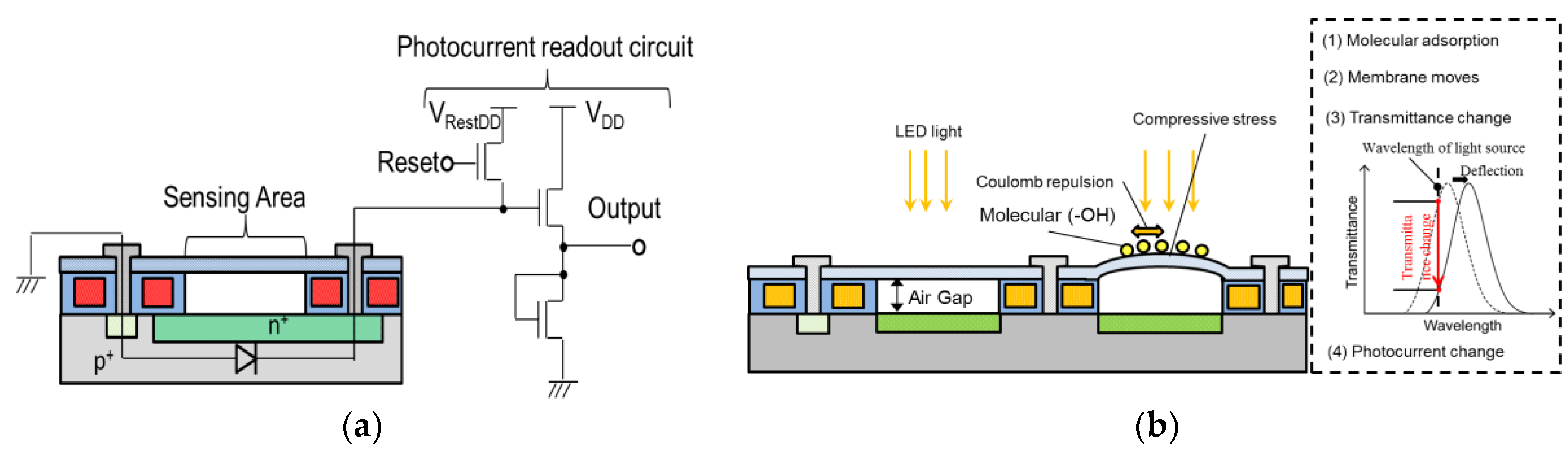
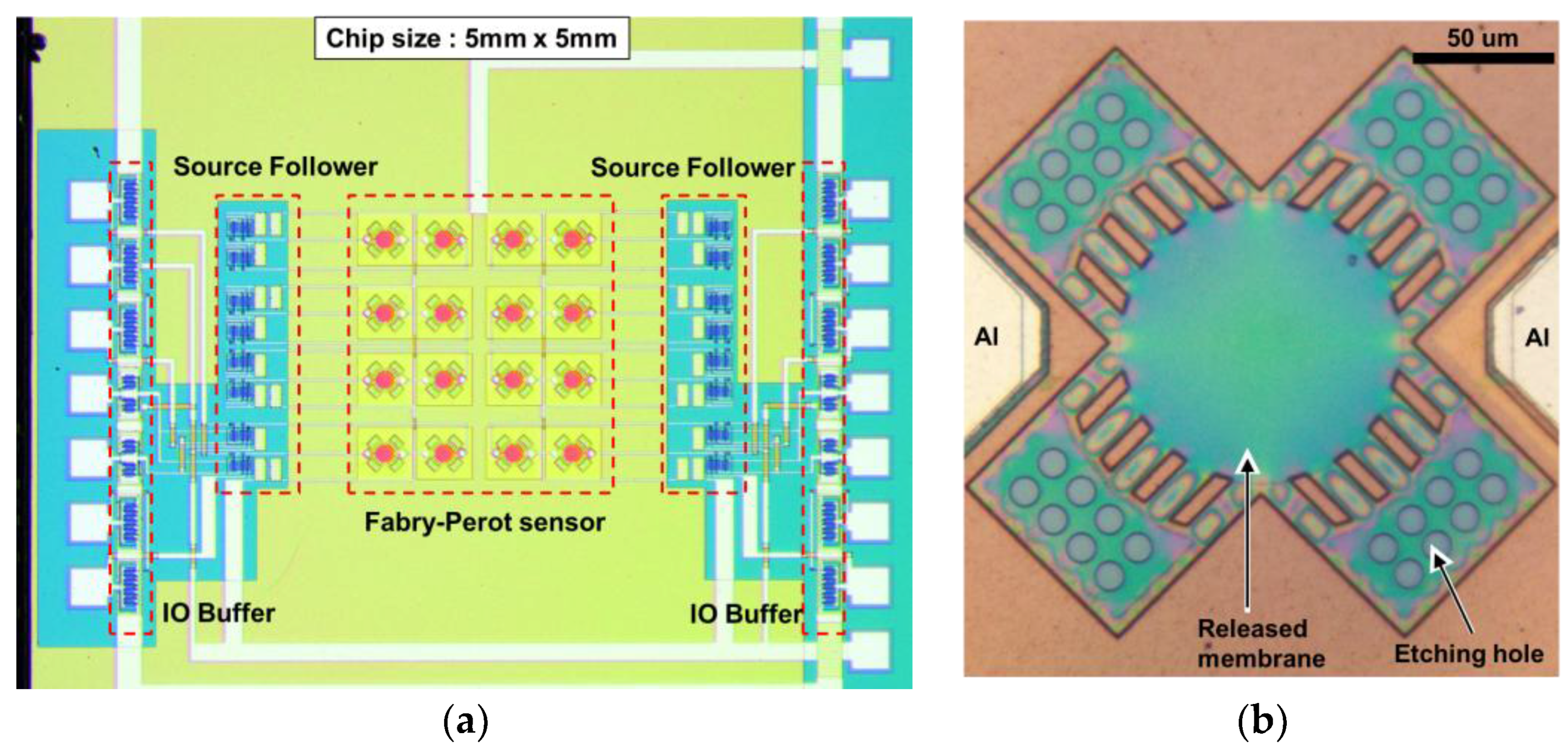
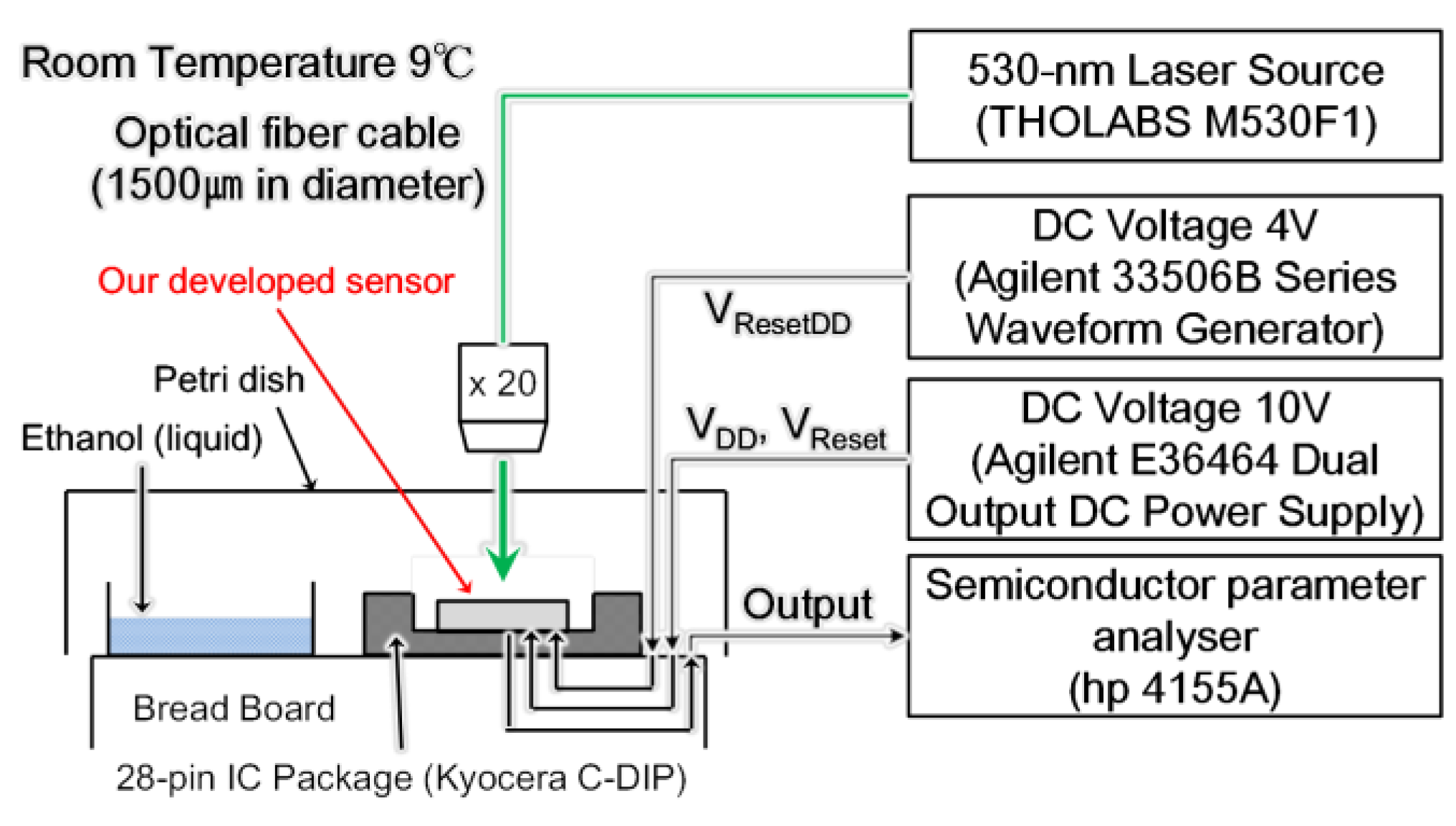
2. Design
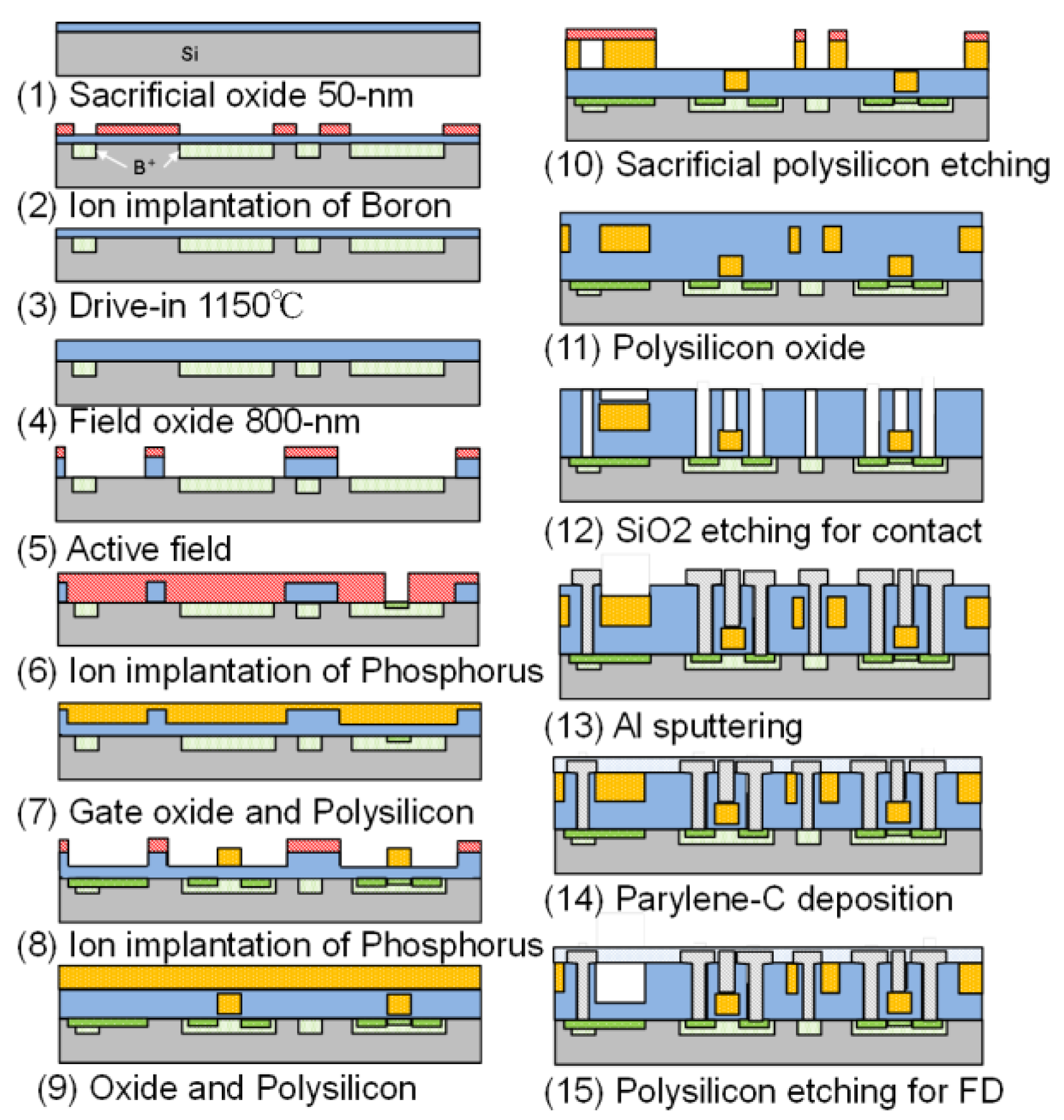
3. Fabrication
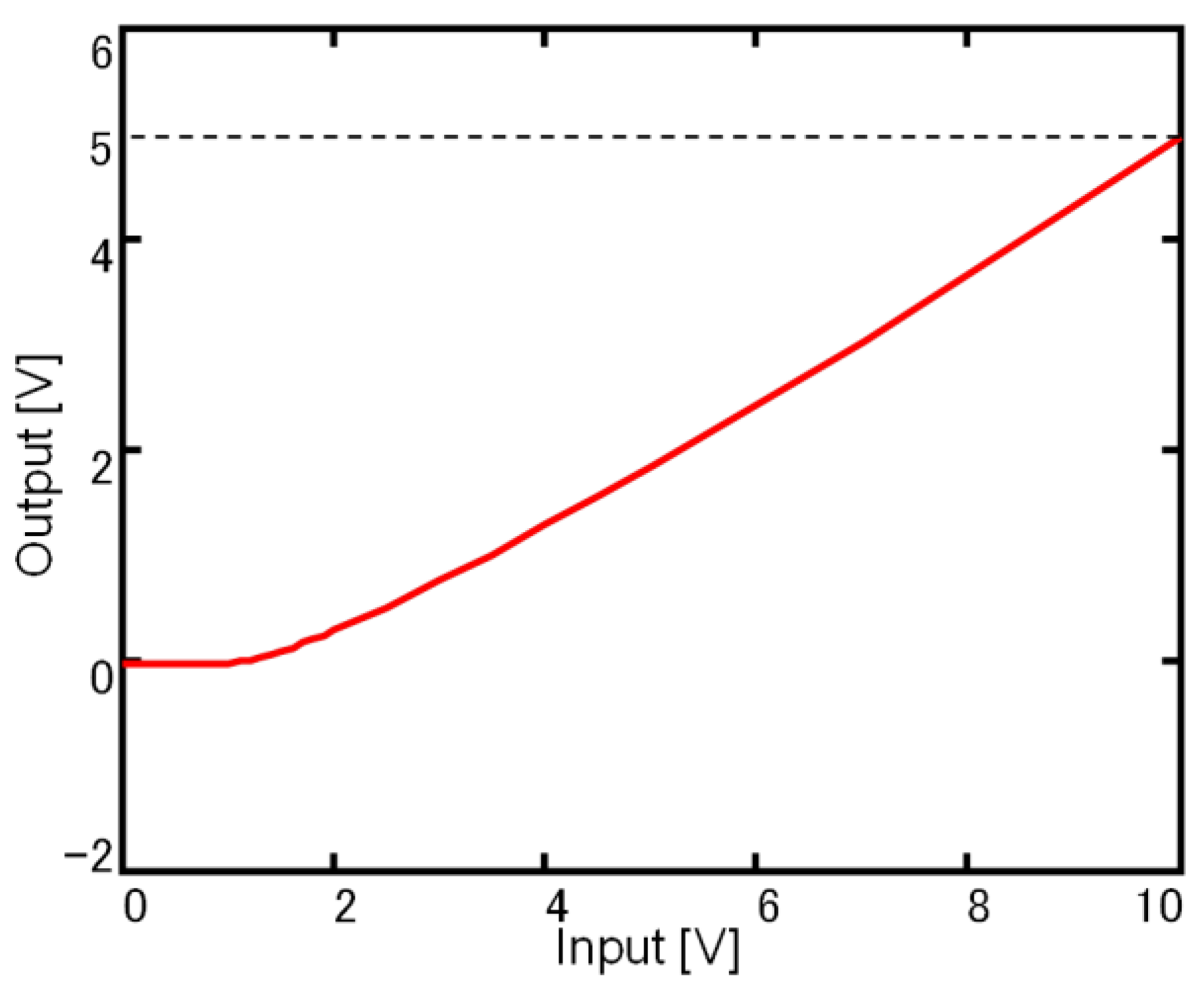
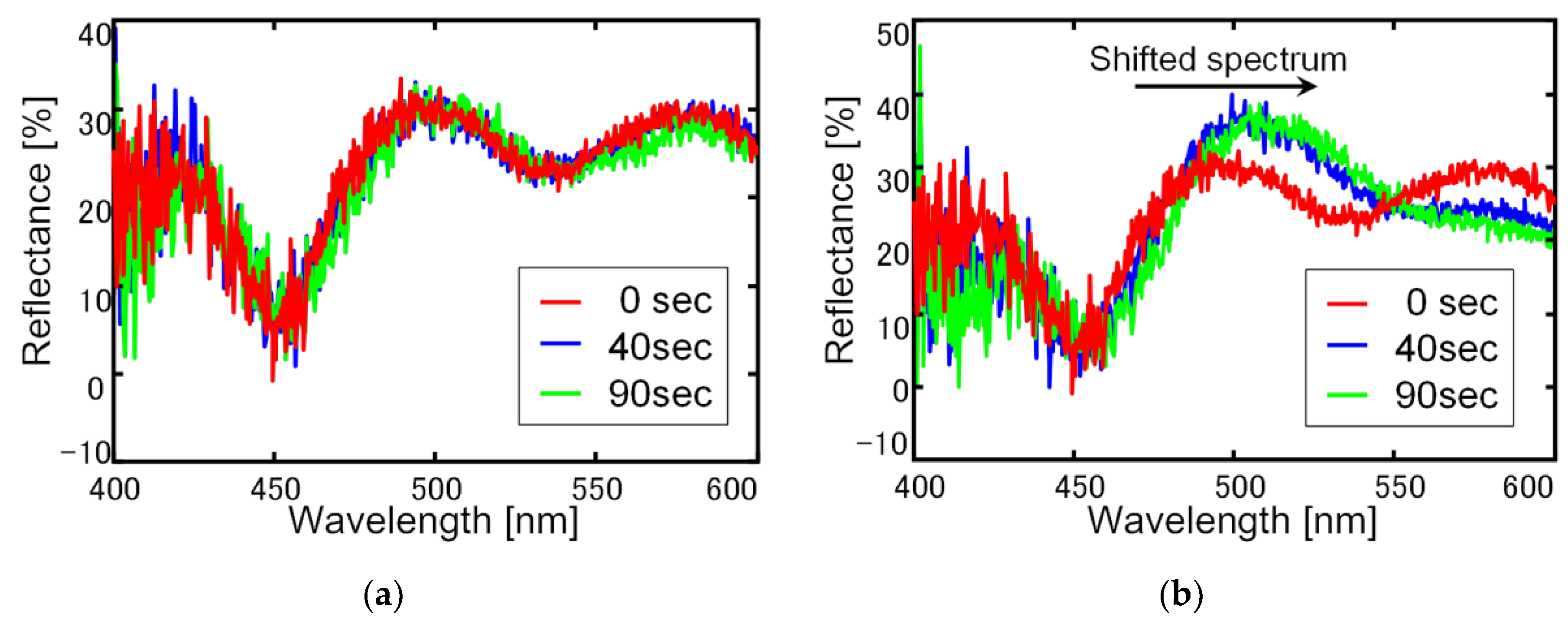
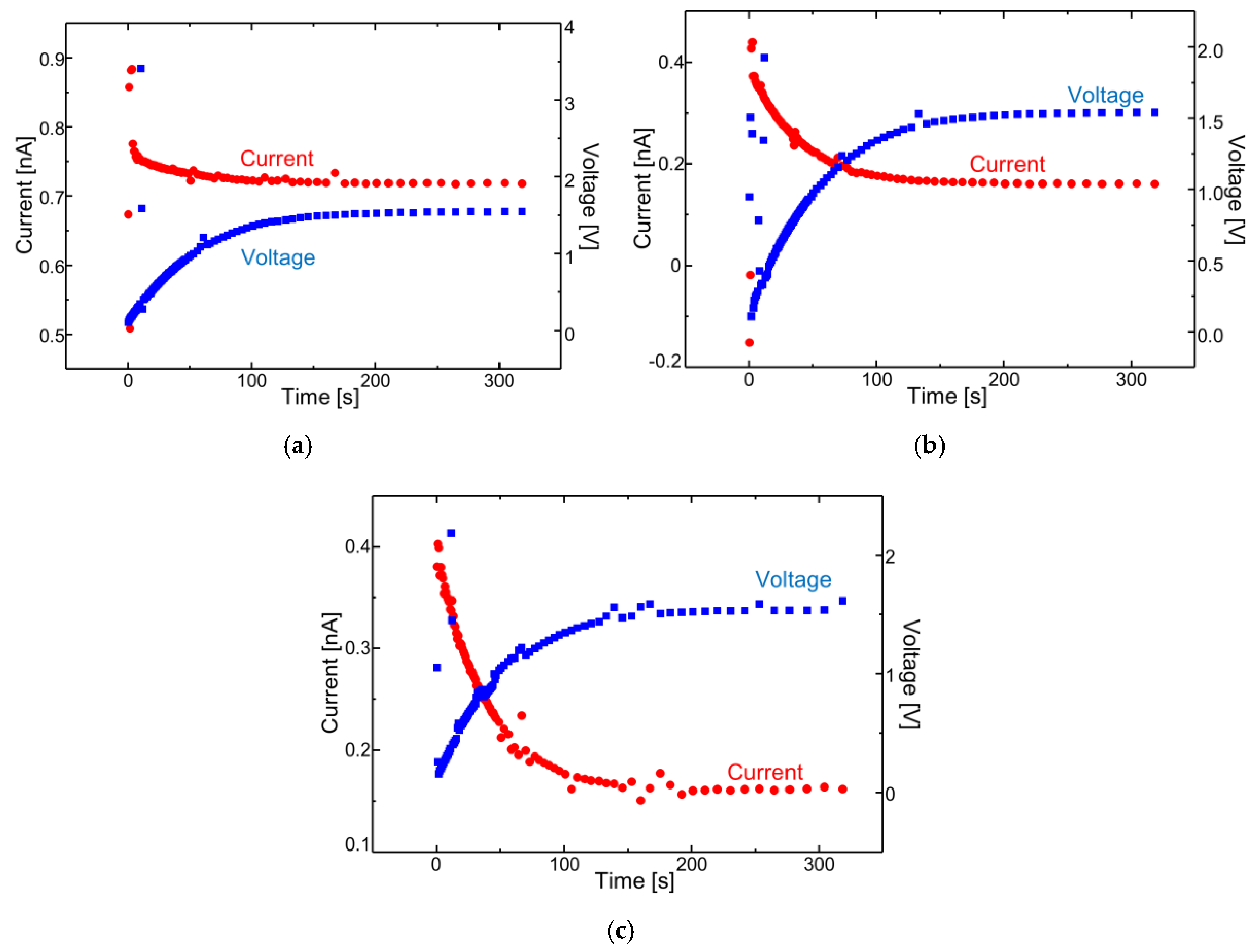
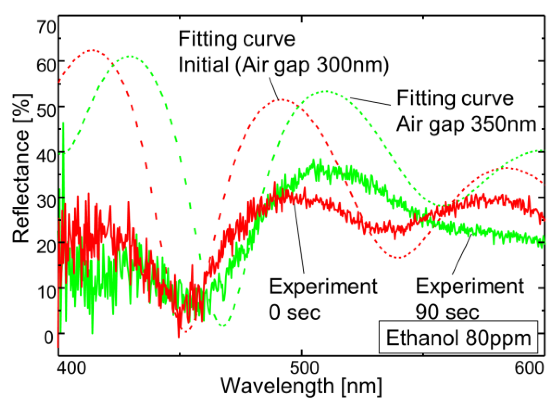
4. Results and Discussion
5. Conclusions
Acknowledgments
Author Contributions
Conflicts of Interest
References
- Barnes, J.R.; Stephenson, R.J.; Welland, M.E.; Gerber, C.; Gimzewski, J.K. Photothermal spectroscopy with femtojoule sensitivity using a micromechanical device. Nature 1994, 79, 6501. [Google Scholar] [CrossRef]
- McKendry, R.; Zhang, J.Y.; Arnt, Y.; Strunz, T.; Hegner, M.; Lang, H.P.; Baller, M.K.; Certa, U.; Meyer, E.; Guntherodt, H.J.; et al. Multiple label-free biodetection and quantitative DNA-binding assays on a nanomechanical cantilever array. Proc. Natl. Acad. Sci. USA 2002, 99, 9783–9788. [Google Scholar] [CrossRef] [PubMed]
- Gimzewski, J.K.; Gerber, C.; Meyer, E.; Schlittler, R.R. Observation of a chemical reaction using a micromechanical sensor. Chem. Phys. Lett. 1994, 217, 589–594. [Google Scholar] [CrossRef]
- Lang, H.P.; Baller, M.K.; Berger, R.; Gerber, C.; Gimzewski, J.K.; Battiston, F.M.; Fornaro, P.; Ramseyer, J.P.; Meyer, E.; Guntherodt, H.J. An artificial nose based on a micromechanical cantilever array. Anal. Chim. Acta 1999, 393, 59–65. [Google Scholar] [CrossRef]
- Berger, R.; Delamarche, E.; Lang, H.P.; Gerber, C.; Gimzewski, J.K.; Meyer, E.; Guntherodt, H.J. Surface stress in the self-assembly of alkanethiols on gold. Science 1997, 276, 2021–2024. [Google Scholar] [CrossRef]
- Fritz, J.; Baller, M.K.; Lang, H.P.; Rothuizen, H.; Vettiger, P.; Meyer, E.; Guntherodt, H.J.; Gerber, C.; Gimzewski, J.K. Translating biomolecular recognition into nanomechanics. Science 2000, 288, 316–318. [Google Scholar] [CrossRef] [PubMed]
- Wu, G.H.; Datar, R.H.; Hansen, K.M.; Thundat, T.; Cote, R.J.; Majumdar, A. Bioassay of prostate-specific antigen (PSA) using microcantilevers. Nat. Biotechnol. 2001, 19, 856–860. [Google Scholar] [CrossRef] [PubMed]
- Yoshikawa, G.; Lang, H.P.; Akiyama, T.; Aeschimann, L.; Staufer, U.; Vettiger, P.; Aono, M.; Sakurai, T.; Gerber, C. Sub-ppm detection of vapors using piezoresistive microcantilever array sensors. Nanotechnology 2009, 20, 015501. [Google Scholar] [CrossRef] [PubMed]
- Yoshikawa, G.; Akiyama, T.; Gautsch, S.; Vettiger, P.; Rohrer, H. Nanomechanical membrane-type surface stress sensor. Nano Lett. 2011, 11, 1044–1048. [Google Scholar] [CrossRef] [PubMed]
- Park, K.K.; Lee, H.; Kupnik, M.; Oralkan, O.; Ramseyer, J.P.; Lang, H.P.; Hegner, M.; Gerber, C.; Khori-Yakub, B.T. Capacitive micromachined ultrasonic transducer (CMUT) as a chemical sensor for DMMP detection. Sens. Actuators B Chem. 2011, 160, 1120–1127. [Google Scholar] [CrossRef]
- Lee, H.J.; Park, K.K.; Kupnik, M.; Khuri-Yakub, B.T. Functionalization layer for CO2 sensing using capacitive micromachined ultrasonic transducers. Sens. Actuators B Chem. 2012, 174, 87–93. [Google Scholar] [CrossRef]
- Karabacak, D.M.; Brongersma, S.H.; Calama, M.C. Enhanced sensitivity volatile detection with low power integrated micromechanical resonators. Lab Chip 2010, 10, 1976–1982. [Google Scholar] [CrossRef] [PubMed]
- Pettine, J.; Patrascu, M.; Karabacak, D.M.; Vandecasteele, M.; Petrescu, V.; Brongersma, S.H.; Calama, M.C.; Van Hoof, C. Volatie detection system using piezoelectric micromechanical resonators interfaced by an oscillator readout. Sens. Actuators A Phys. 2013, 189, 496–503. [Google Scholar] [CrossRef]
- Backmann, N.; Zahnd, C.; Huber, F.; Bietsch, A.; Pluckthun, A.; Lang, H.P.; Guntherodt, H.J.; Hegner, M.; Gerber, C. A label-free immunosensor array using single-chain antibody fragments. Proc. Natl. Acad. Sci. USA 2005, 102, 14587–14592. [Google Scholar] [CrossRef] [PubMed]
- Zhang, J.; Lang, H.P.; Huber, F.; Bietsch, A.; Grange, W.; Certa, U.; McKendry, R.; Guntherodt, H.J.; Hegner, M.; Gerber, C. Rapid and label-free nanomechanical detection of biomarker transcripts in human RNA. Nat. Nanotechnol. 2006, 1, 214–220. [Google Scholar] [CrossRef] [PubMed]
- Raorane, D.A.; Lim, M.D.; Chen, F.F.; Craik, C.S.; Majumdar, A. Quantitative and label-free technique for measuring protease activity and inhibition using a microfluidic cantilever array. Nano Lett. 2008, 8, 2968–2974. [Google Scholar] [CrossRef] [PubMed]
- Ghatkesar, M.K.; Lang, H.P.; Gerber, C.; Hegner, M.; Braun, T. Comprehensive characterization of molecular interactions based on nanomechanics. PLoS ONE 2008, 3, e3610. [Google Scholar] [CrossRef] [PubMed]
- Mukhopadhyay, R.; Sumbayev, V.V.; Lorentzen, M.; Kjems, J.; Andreasen, P.A.; Besenbacher, F. Cantilever sensor for nanomechanical detection of specific protein conformations. Nano Lett. 2005, 5, 2385–2388. [Google Scholar] [CrossRef] [PubMed]
- Arlett, J.L.; Maloney, J.R.; Gudlewski, B.; Muluneh, M.; Roukes, M.L. Self-sensing micro- and nanocantilevers with attonewton-scale force resolution. Nano Lett. 2006, 6, 1000–1006. [Google Scholar] [CrossRef]
- Tortonese, M.; Barrett, R.C.; Quate, C.F. Atomic resolution with an atomic force microscope using piezoresistive detection. Appl. Phys. Lett. 1993, 62, 834–836. [Google Scholar] [CrossRef]
- Aeschimann, L.; Meister, A.; Akiyama, T.; Chui, B.W.; Niedermann, P.; Heinzelmann, H.; De Rooij, N.F.; Staufer, U.; Vettiger, P. Scanning probe arrays for life sciences and nanobiology applications. Microelectron. Eng. 2006, 83, 1698–1701. [Google Scholar] [CrossRef]
- Takahashi, K.; Ozawa, R.; Oyama, H.; Futagawa, M.; Dasai, F.; Ishida, M.; Sawada, K. A CMOS-MEMS-based label-free protein sensor for high-sensitive and compact system. In Proceedings of the IEEE International Electron Devices Meeting, San Francisco, CA, USA, 10–13 December 2012; pp. 553–556. [Google Scholar]

© 2018 by the authors. Licensee MDPI, Basel, Switzerland. This article is an open access article distributed under the terms and conditions of the Creative Commons Attribution (CC BY) license (http://creativecommons.org/licenses/by/4.0/).
Share and Cite
Maruyama, S.; Hizawa, T.; Takahashi, K.; Sawada, K. Optical-Interferometry-Based CMOS-MEMS Sensor Transduced by Stress-Induced Nanomechanical Deflection. Sensors 2018, 18, 138. https://doi.org/10.3390/s18010138
Maruyama S, Hizawa T, Takahashi K, Sawada K. Optical-Interferometry-Based CMOS-MEMS Sensor Transduced by Stress-Induced Nanomechanical Deflection. Sensors. 2018; 18(1):138. https://doi.org/10.3390/s18010138
Chicago/Turabian StyleMaruyama, Satoshi, Takeshi Hizawa, Kazuhiro Takahashi, and Kazuaki Sawada. 2018. "Optical-Interferometry-Based CMOS-MEMS Sensor Transduced by Stress-Induced Nanomechanical Deflection" Sensors 18, no. 1: 138. https://doi.org/10.3390/s18010138
APA StyleMaruyama, S., Hizawa, T., Takahashi, K., & Sawada, K. (2018). Optical-Interferometry-Based CMOS-MEMS Sensor Transduced by Stress-Induced Nanomechanical Deflection. Sensors, 18(1), 138. https://doi.org/10.3390/s18010138