
Microfabrication and Integration of a Sol-Gel PZT Folded Spring Energy Harvester

Abstract
:1. Introduction
2. Microfabrication of PZT Sol-Gel Folded Spring Energy Harvesters
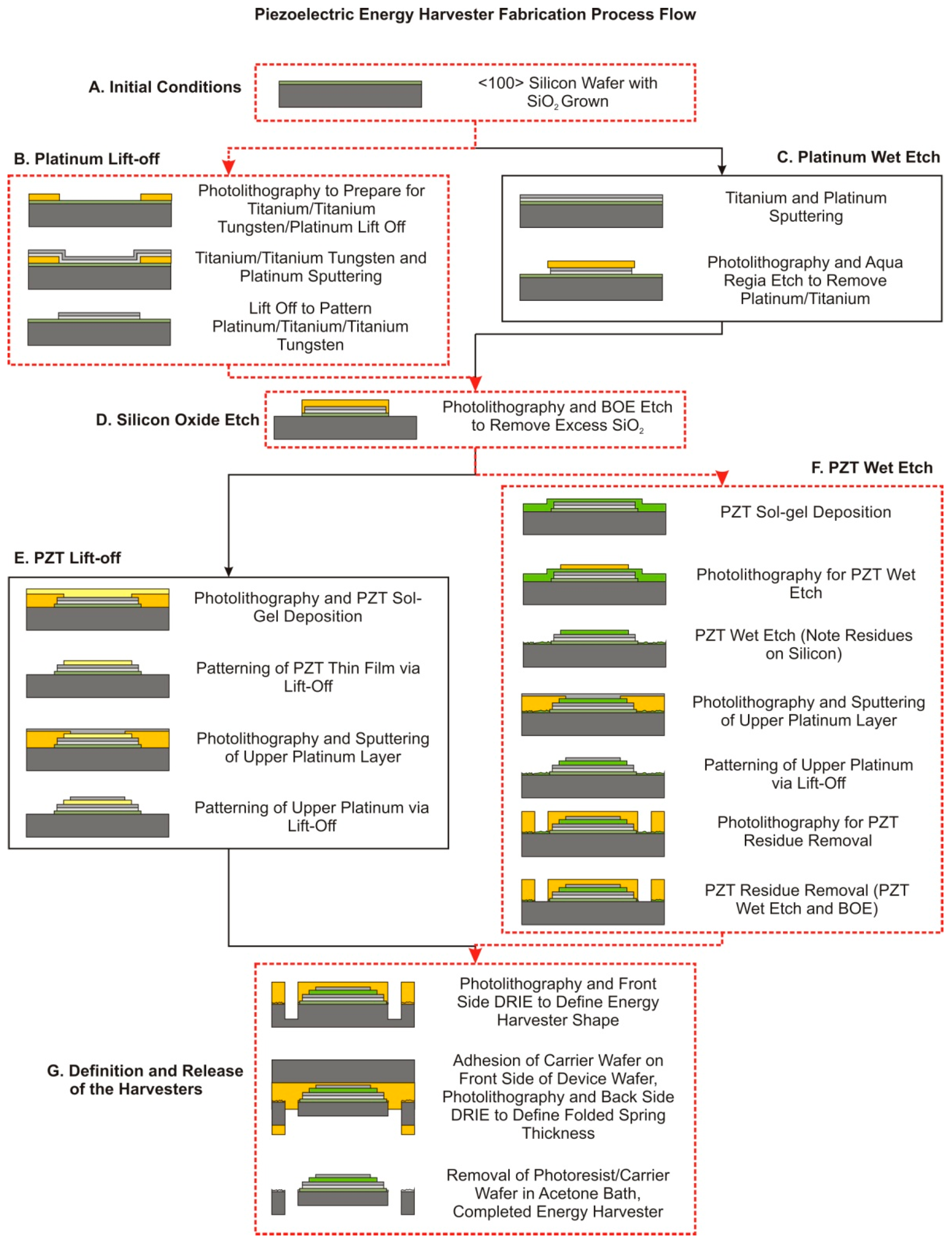
2.1. Energy Harvester Microfabrication Process Flow Overview
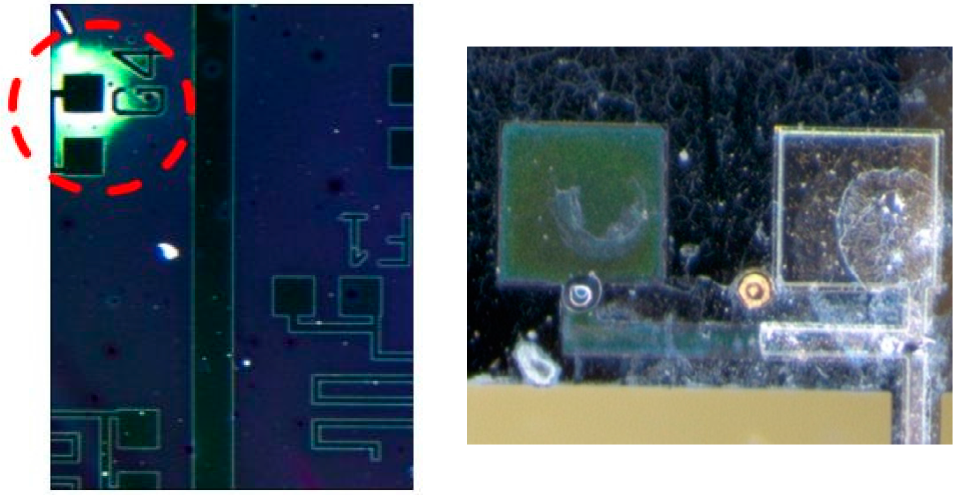
2.2. Lower Electrode Deposition Process Challenges

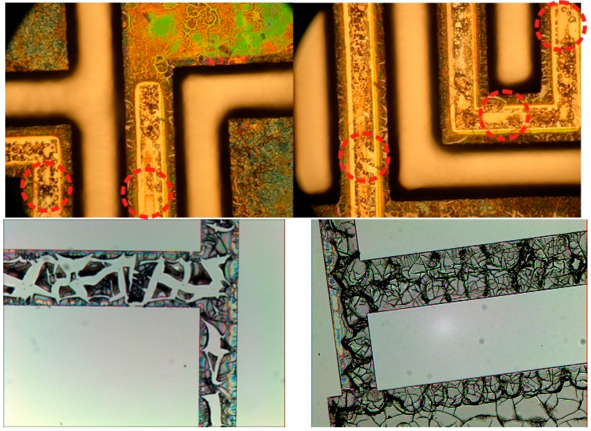
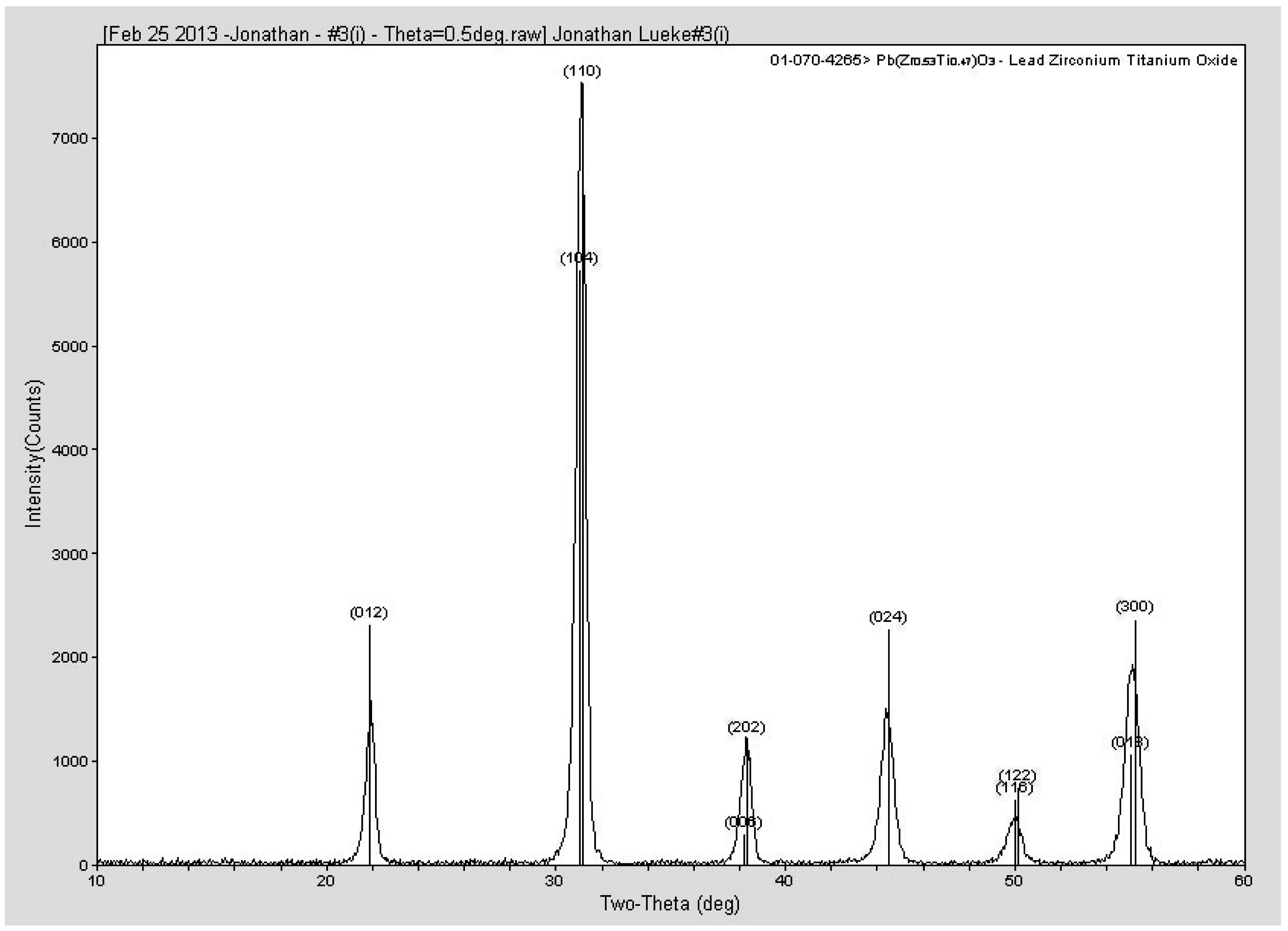
2.3. PZT Sol-Gel Deposition and Patterning Challenges

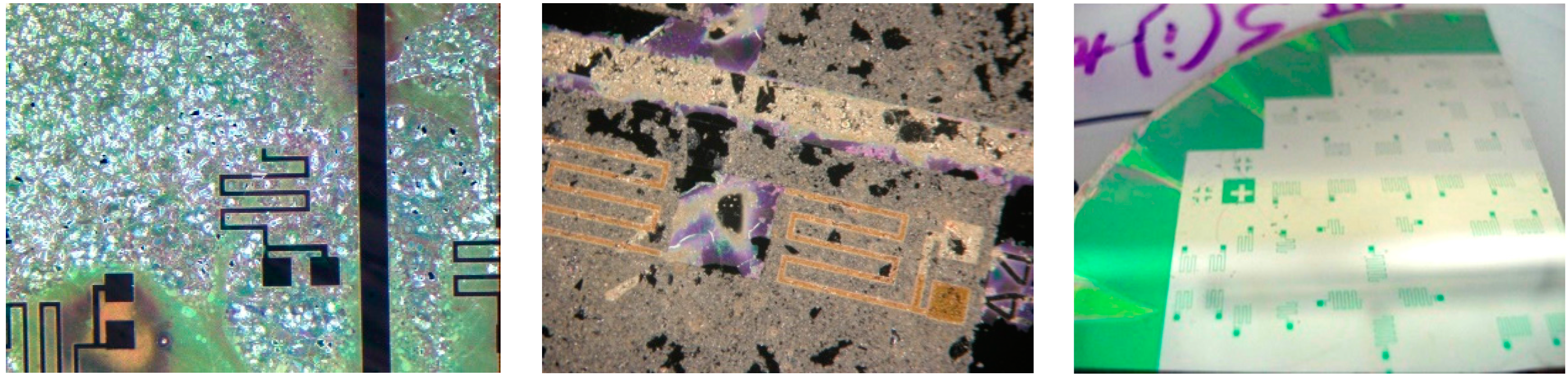
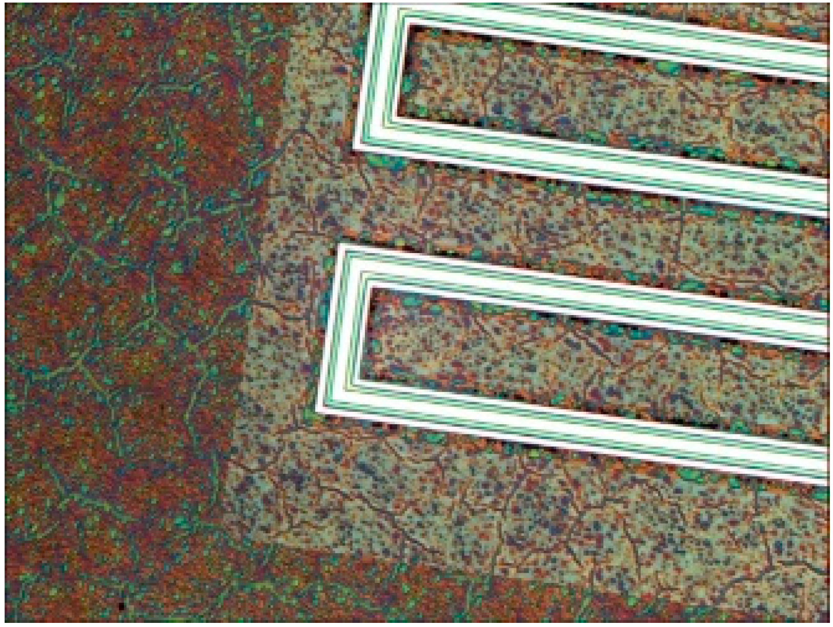
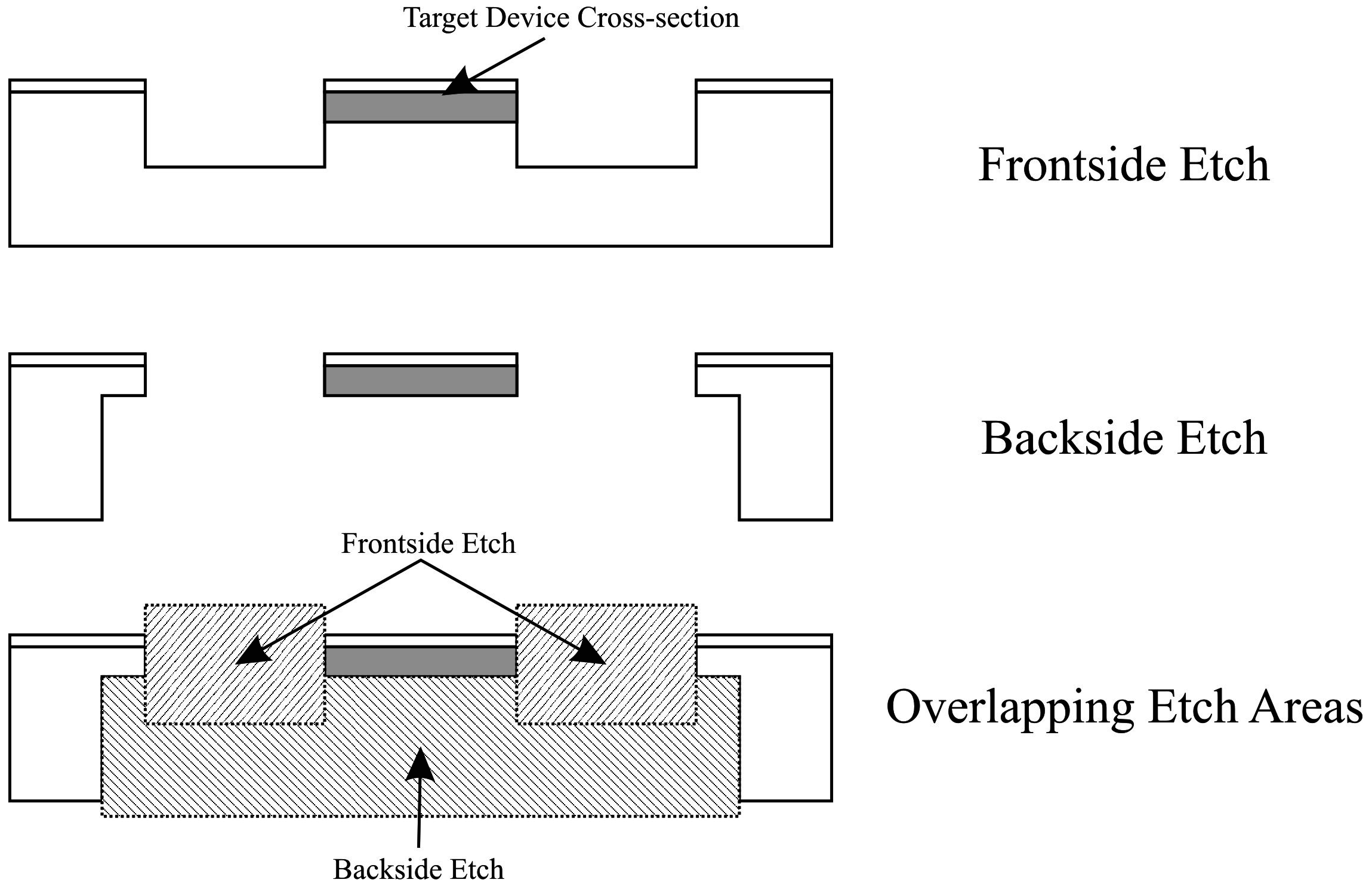
2.4. Challenges Involved with Definition and Release of the Energy Harvesters

3. Packaging and Integration of the Energy Harvesters
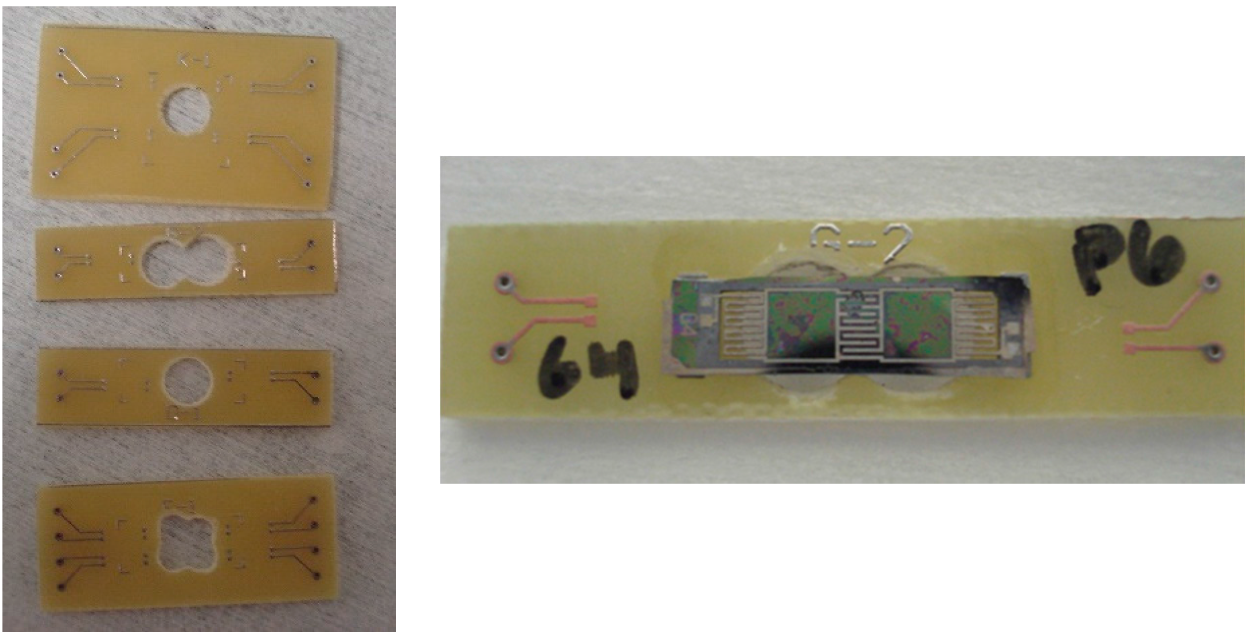
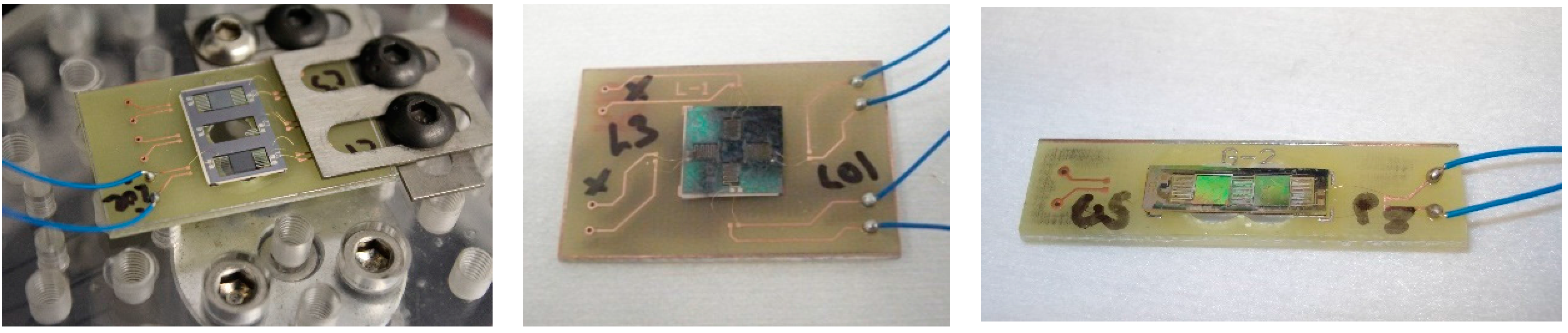
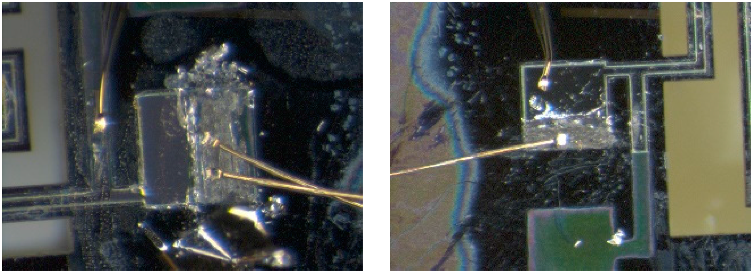
3.1. Overview of the Packaging Methodology for the Energy Harvesters
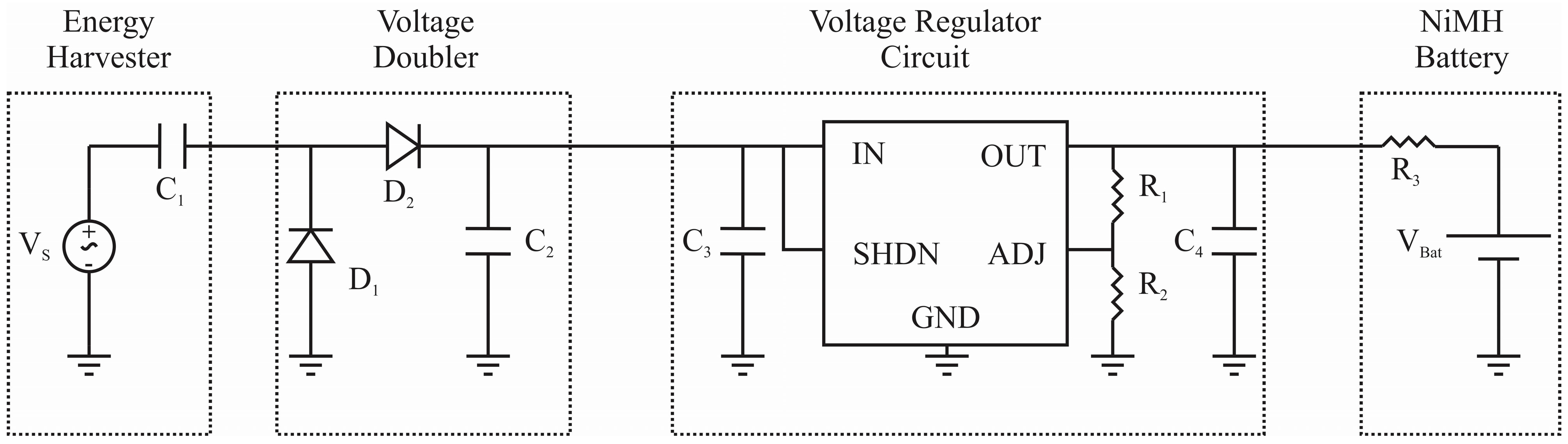
3.2. Overview of the Conditioning Circuitry for the Energy Harvesters
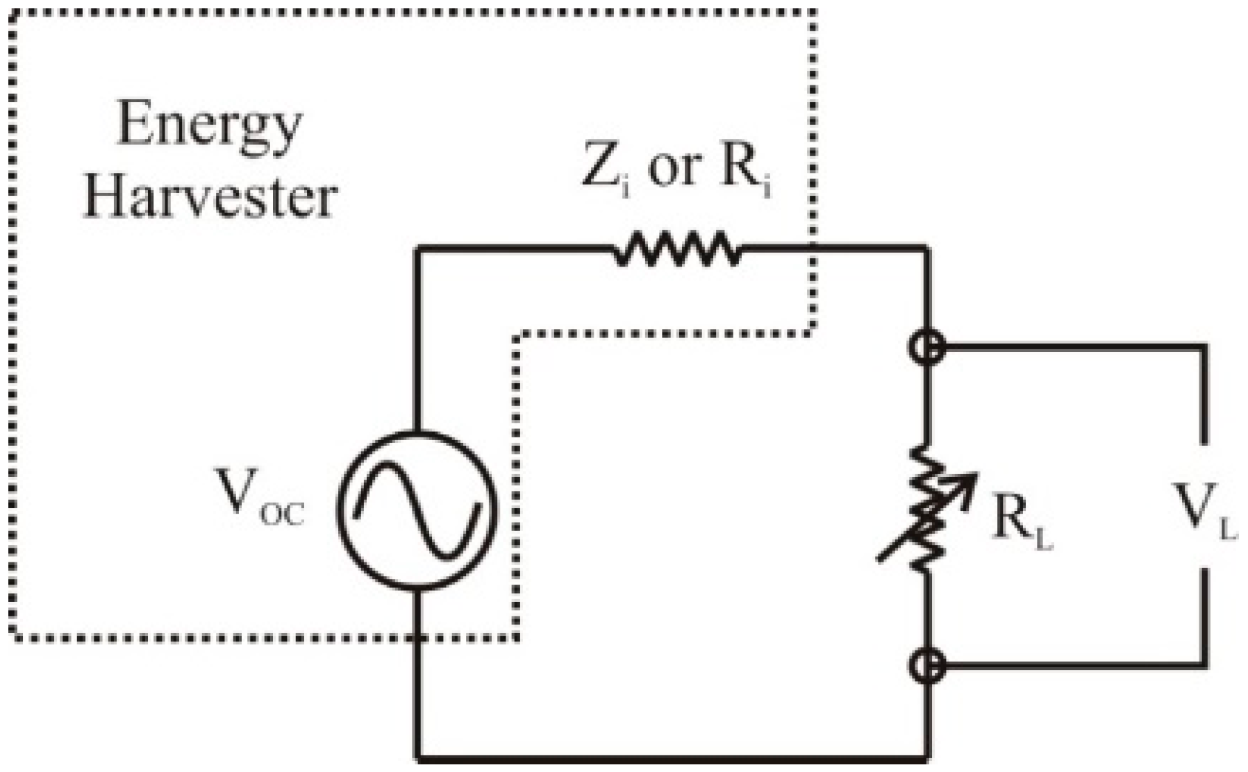
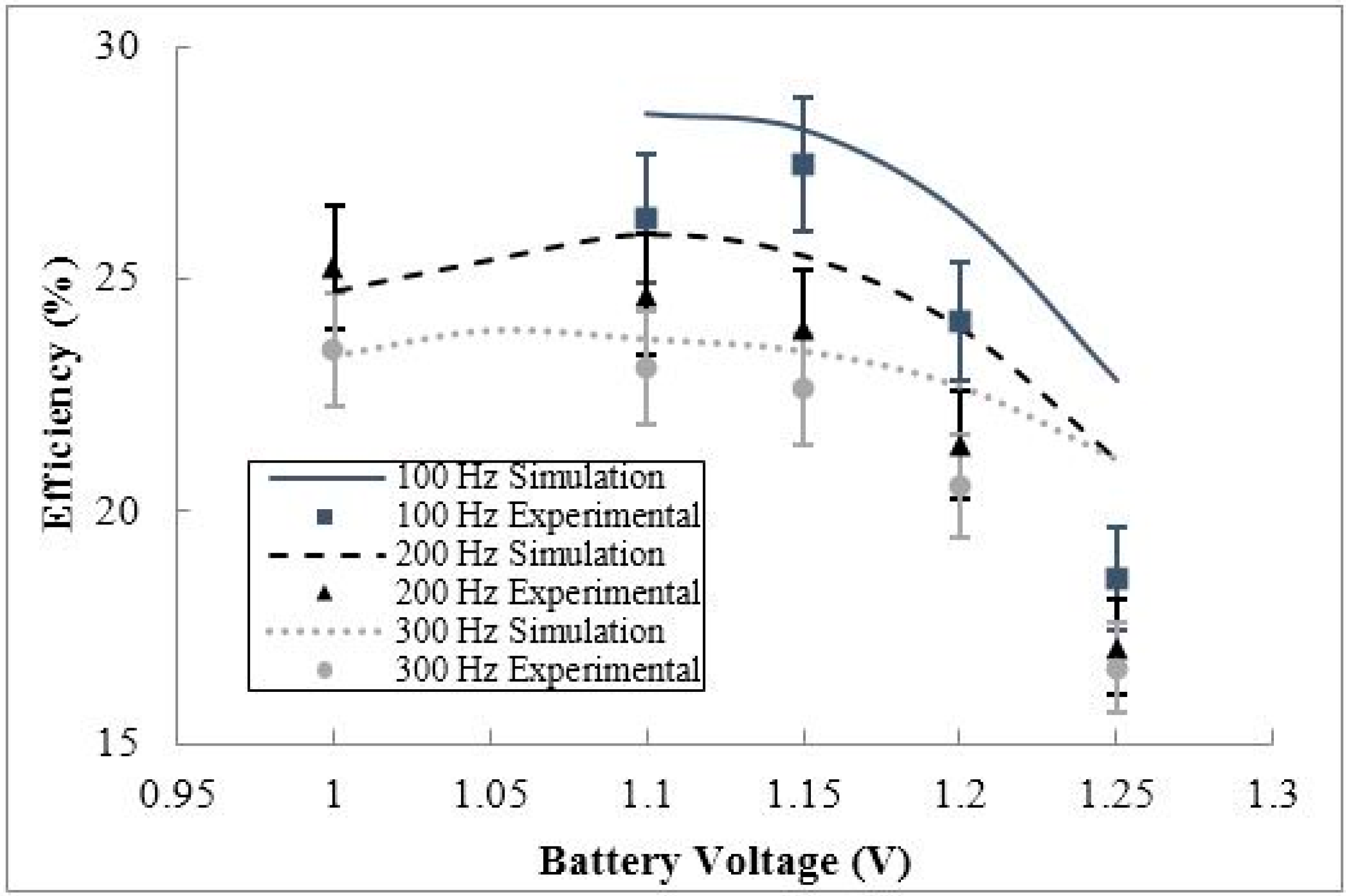
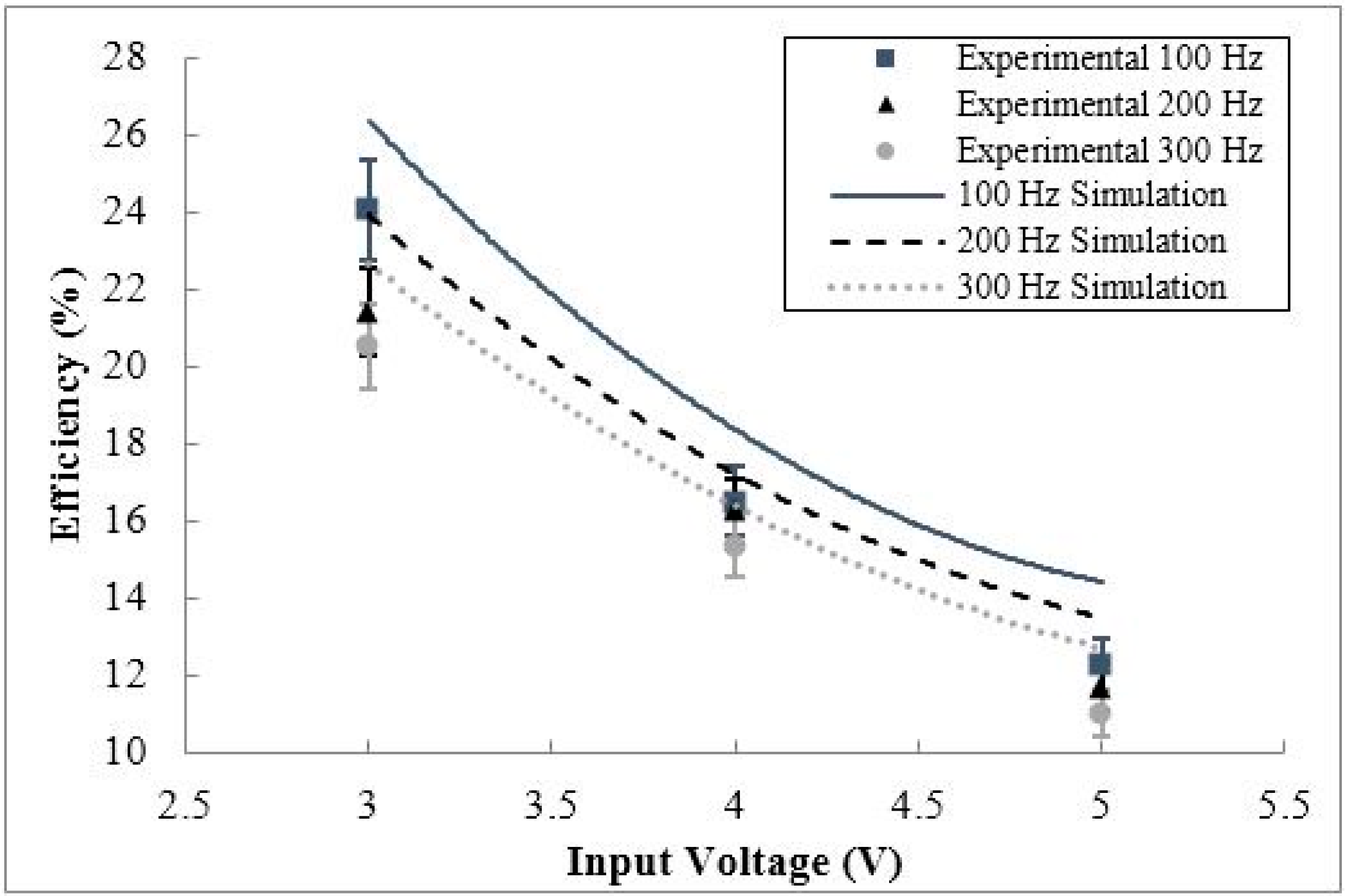
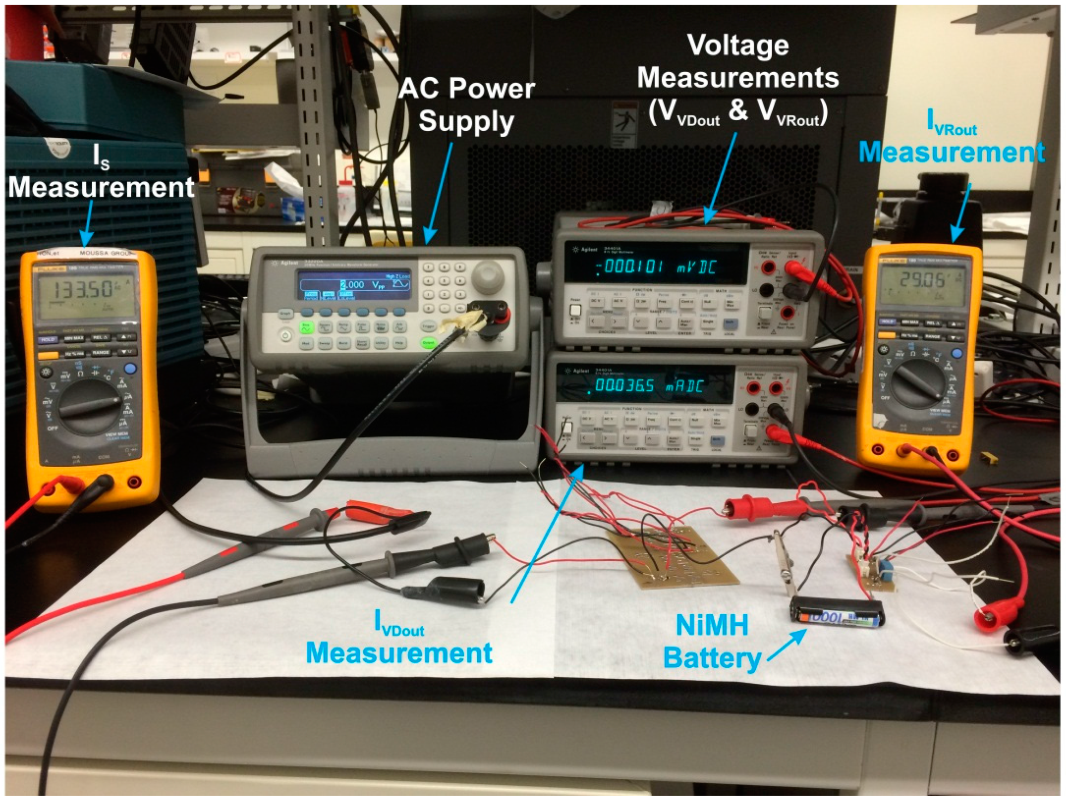
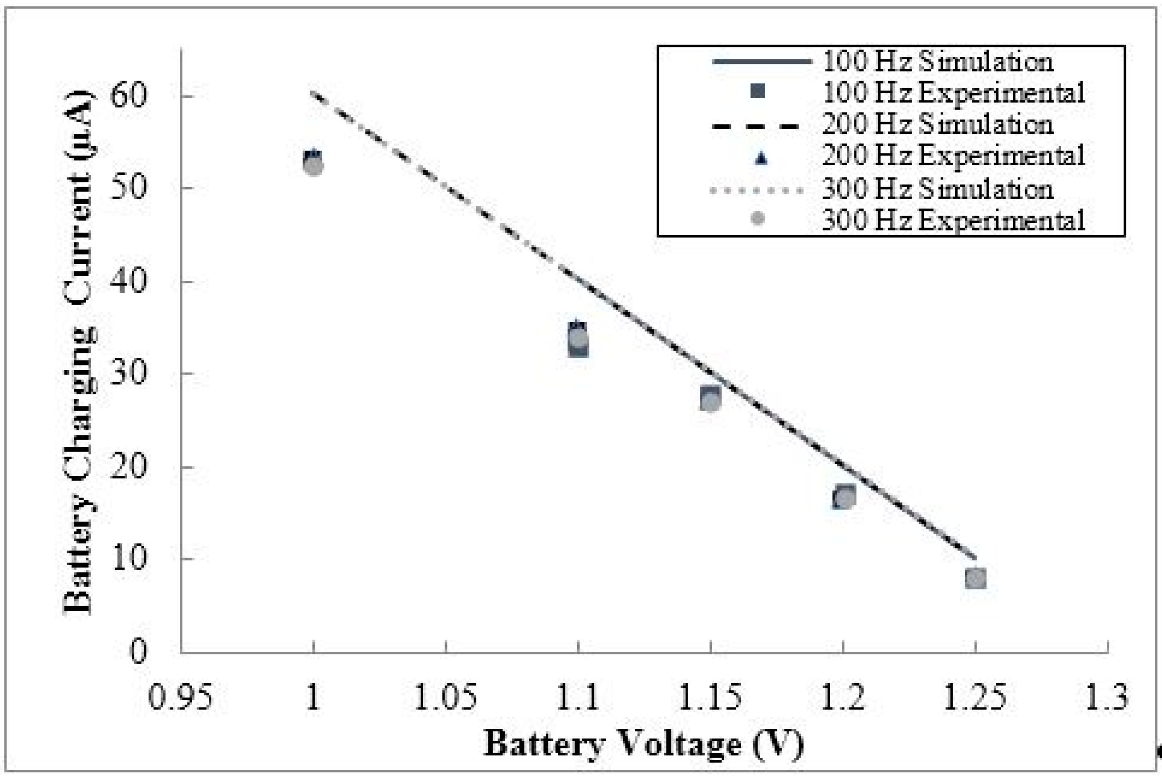
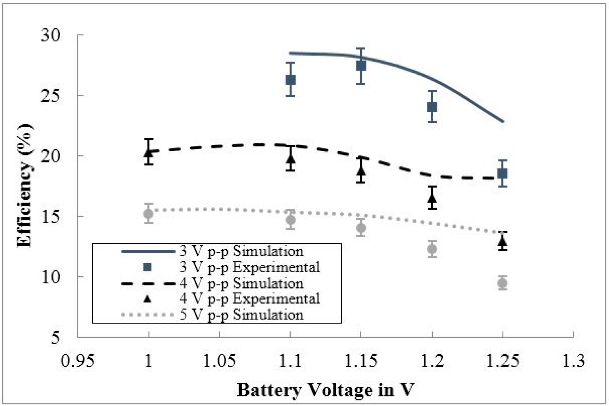
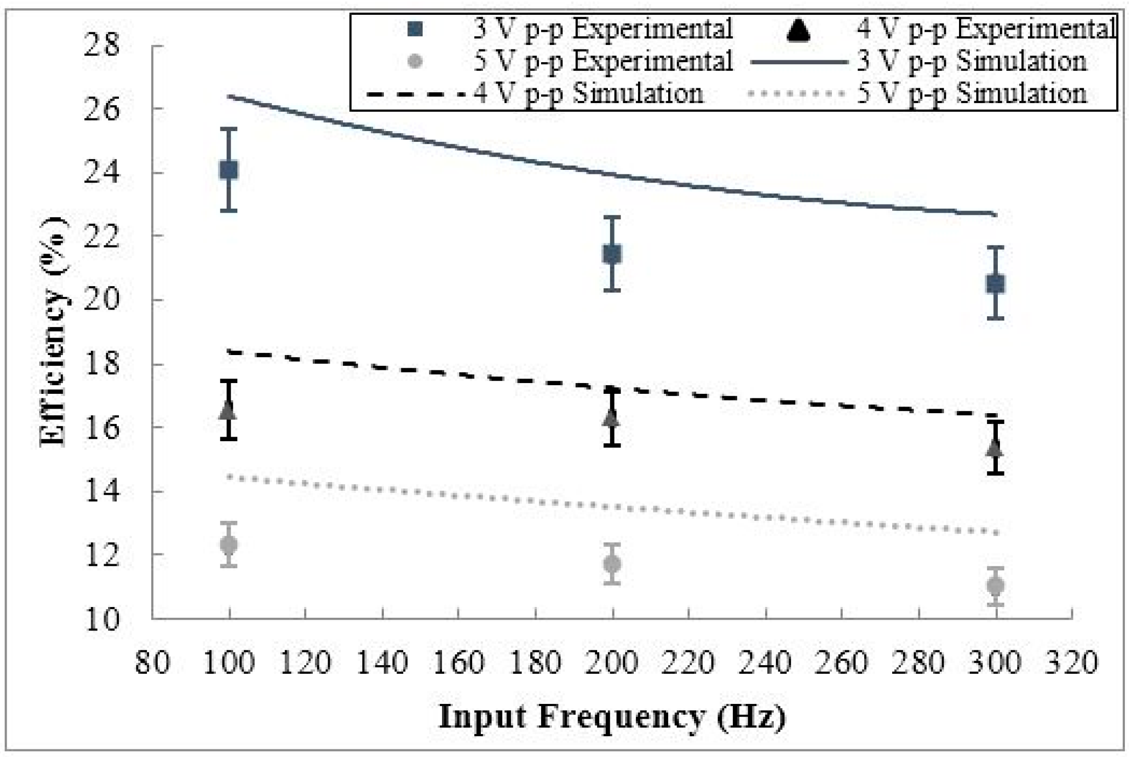
3.3. Feasibility Study of the Conditioning Circuitry


4. Conclusions
Acknowledgments
Author Contributions
Conflicts of Interest
References
- Lueke, J.; Moussa, W.A. Mems-based power generation techniques for implantable biosensing applications. Sensors 2011, 11, 1433–1460. [Google Scholar] [CrossRef] [PubMed]
- Roundy, S.; Leland, E.S.; Baker, J.; Carleton, E.; Reilly, E.; Lai, E.; Otis, B.; Rabaey, J.M.; Wright, P.K.; Sundararajan, V. Improving power output for vibration-based energy scavengers. IEEE Pervasive Comput. 2005, 4, 28–36. [Google Scholar] [CrossRef]
- Roundy, S.; Wright, P.K. A piezoelectric vibration based generator for wireless electronics. Smart Mater. Struct. 2004, 13, 1131–1142. [Google Scholar] [CrossRef]
- Cook-Chennault, K.A.; Thambi, N.; Sastry, A.M. Powering mems portable devices—A review of non-regenerative and regenerative power supply systems with special emphasis on piezoelectric energy harvesting systems. Smart Mater. Struct. 2008, 17. [Google Scholar] [CrossRef]
- Lueke, J.; Rezaei, M.; Moussa, W.A. Investigation of folded spring structures for vibration-based piezoelectric energy harvesting. J. Micromech. Microeng. 2014. [Google Scholar] [CrossRef]
- Lee, K.B. Statics. In Principles of Microelectromechanical Systems; John Wiley & Sons, Inc.: Hoboken, NJ, USA, 2011; pp. 64–143. [Google Scholar]
- Lee, K.B. Static behavior of microstructures. In Principles of Microelectromechanical Systems; John Wiley & Sons, Inc.: Hoboken, NJ, USA, 2011; pp. 144–234. [Google Scholar]
- Lee, K.B. Dynamics. In Principles of Microelectromechanical Systems; John Wiley & Sons, Inc.: Hoboken, NJ, USA, 2011; pp. 235–324. [Google Scholar]
- Lueke, J. A Mems-Based Fixed-Fixed Folded Spring Piezoelectric Energy Harvester. Ph.D. Theis, University of Alberta, Edmonton, AB, Canada, 2014. [Google Scholar]
- Boisseau, S.; Despesse, G.; Ricart, T.; Defay, E.; Sylvestre, A. Cantilever-based electret energy harvesters. Smart Mater. Struct. 2011, 20. [Google Scholar] [CrossRef]
- Casset, F.; Cueff, M.; Suhm, A.; Le Rhun, G.; Abergel, J.; Allain, M.; Dieppedale, C.; Ricart, T.; Fanget, S.; Renaux, P.; et al. Pzt piezoelectric coefficient extraction by pzt-actuated micro-beam characterization and modeling. In Proceedings of the 2012 13th International Conference on Thermal, Mechanical and Multi-Physics Simulation and Experiments in Microelectronics and Microsystems (EuroSimE), Cascais, Portugal, 16–18 April 2012; pp. 1/4–4/4.
- Ettelt, D.; Dodane, G.; Audoin, M.; Walther, A.; Jourdan, G.; Rey, P.; Robert, P.; Delamare, J. A novel microfabricated high precision vector magnetometer. In Proceedings of the 2011 IEEE Sensors, Limerick, Ireland, 28–31 October 2011; pp. 2010–2013.
- Ettelt, D.; Rey, P.; Savoye, M.; Coutier, C.; Cartier, M.; Redon, O.; Audoin, M.; Walther, A.; Robert, P.; Zhang, Y.; et al. A new low consumption 3D compass using integrated magnets and piezoresistive nano-gauges. In Proceedings of the 2011 16th International Solid-State Sensors, Actuators and Microsystems Conference (TRANSDUCERS), Beijing, China, 5–9 June 2011; pp. 40–43.
- Jeon, Y.B.; Sood, R.; Jeong, J.H.; Kim, S.G. Mems power generator with transverse mode thin film pzt. Sens. Actuators A Phys. 2005, 122, 16–22. [Google Scholar] [CrossRef]
- Ricart, T.; Lassagne, P.; Boisseau, S.; Despesse, G.; Lefevre, A.; Billard, C.; Fanget, S.; Defay, E. Macro energy harvester based on aluminium nitride thin films. In Proceedings of the 2011 IEEE International Ultrasonics Symposium (IUS), Orlando, FL, USA, 18–21 October 2011; pp. 1928–1931.
- Yin, S.; Abergel, J.; Bontempi, A.; Ricart, T.; Le Rhun, G.; Defay, E.; Niu, G.; Vilquin, B.; Gautier, B.; Robach, Y. Single crystal pzt thin film membrane with highly conductive electrodes. In Proceedings of the 2012 IEEE International Ultrasonics Symposium (IUS), Dresden, Germany, 7–10 October 2012; pp. 792–794.
- Elfrink, R.; Kamel, T.M.; Goedbloed, M.; Matova, S.; Hohlfeld, D.; van Andel, Y.; van Schaijk, R. Vibration energy harvesting with aluminum nitride-based piezoelectric devices. J. Micromech. Microeng. 2009, 19. [Google Scholar] [CrossRef]
- Miller, L.M.; Halvorsen, E.; Dong, T.; Wright, P.K. Modeling and experimental verification of low-frequency mems energy harvesting from ambient vibrations. J. Micromech. Microeng. 2011, 21, 045029. [Google Scholar] [CrossRef]
- Rezaei, M.; Lueke, J.; Raboud, D.; Moussa, W. Challenges in fabrication and testing of piezoelectric mems with a particular focus on energy harvesters. Microsyst. Technol. 2013, 19, 1–25. [Google Scholar] [CrossRef]
- Williams, K.R.; Gupta, K.; Wasilik, M. Etch rates for micromachining processing—Part II. J. Microelectromech. Syst. 2003, 12, 761–778. [Google Scholar] [CrossRef]
- Zheng, K.; Lu, J.; Chu, J. A novel wet etching process of Pb(Zr,Ti)O3 thin films for applications in microelectromechanical system. Jpn. J. Appl. Phys. 2004, 43, 3934–3937. [Google Scholar] [CrossRef]
- Ohring, M. Chapter 11—interdiffusion, reactions, and transformations in thin films. In Materials Science of Thin Films, 2nd ed.; Academic Press: San Diego, CA, USA, 2002; pp. 641–710. [Google Scholar]
- Jensen, S.; Jensen, J.M.; Quaade, U.J.; Hansen, O. Uniformity-improving dummy structures for deep reactive ion etching (drie) processes. In Progress in Biomedical Optics and Imaging—Proceedings of SPIE, San Jose, CA, USA; Maher, M.A., Stewart, H.D., Eds.; 2005; pp. 39–46. [Google Scholar]
- Laermer, F.; Schilp, A. Method of anisotropically etching silicon. U.S. Patent 5,501,893 A, 26 Mar 1996. [Google Scholar]
- Sun, H.; Hill, T.; Schmidt, M.; Boning, D. Characterization and modeling of wafer and die level uniformity in deep reactive ion etching (drie). Mater. Res. Soc. Symp. Proc. 2004, 782, A1021–A1026. [Google Scholar] [CrossRef]
- Madou, M.J. Fundamentals of Microfabrication: The Science of Miniturization, 2nd ed.; CRC Press: Boca Raton, FL, USA, 2002; p. 723. [Google Scholar]
- Senturia, S. Microsystem Design, 1st ed.; Kluwer Academic Publishers: Boston, MA, USA, 2001. [Google Scholar]
- Zhu, H.; Miao, J.; Chen, B.; Wang, Z.; Zhu, W. Membrane microcantilever arrays fabrication with pzt thin films for nanorange movement. Microsyst. Technol. 2005, 11, 1121–1126. [Google Scholar] [CrossRef]
- Sakmen, U.; Stranz, A.; Fandling, S.; Wehmann, H.H.; Bandalo, V.; Bora, A.; Tornow, M.; Waag, A.; Peiner, E. Capabilities of icp-rie cryogenic dry etching of silicon: Review of exemplary microstructures. J. Micromech. Microeng. 2009, 19. [Google Scholar] [CrossRef]
- Oliver, A.D.; Wallner, T.A.; Tandon, R.; Nieman, K.; Bergstrom, P.L. Diamond scribing and breaking of silicon for mems die separation. J. Micromech. Microeng. 2008, 18. [Google Scholar] [CrossRef]
- Overstolz, T.; Clerc, P.A.; Noell, W.; Zickar, M.; de Rooij, N.F. A clean wafer-scale chip-release process without dicing based on vapor phase etching. In Proceedings of the IEEE International Conference on Micro Electro Mechanical Systems (MEMS), Maastricht, The Netherlands, 25–29 January 2004; pp. 717–720.
- Sari, I.; Zeimpekis, I.; Kraft, M. A dicing free soi process for mems devices. Microelectron. Eng. 2012, 95, 121–129. [Google Scholar] [CrossRef]
- Rezaei, M.; Lueke, J.; Sameoto, D.; Raboud, D.; Moussa, A. A new approach to cleave mems devices from silicon substrates. J. Mech. Eng. Autom. 2013, 3, 731–738. [Google Scholar]
- Benfield, D.; Lueke, J.; Moussa, W.A. Mems packaging using flexible printed circuit boards. CMC Packag. Appl. Note 2011. [Google Scholar]
- Irwin, J.D.; Wu, C.H. Basic Engineering Circuit Analysis, 6th ed.; Prentice-Hall, Inc.: Upper Sadle River, NJ, USA, 1999; p. 976. [Google Scholar]
- Ramadass, Y.K.; Chandrakasan, A.P. An efficient piezoelectric energy harvesting interface circuit using a bias-flip rectifier and shared inductor. IEEE J. Solid State Circuits 2010, 45, 189–204. [Google Scholar] [CrossRef]
- Qiu, J.; Jiang, H.; Ji, H.; Zhu, K. Comparison between four piezoelectric energy harvesting circuits. Front. Mech. Eng. China 2009, 4, 153–159. [Google Scholar] [CrossRef]
- Szarka, G.D.; Stark, B.H.; Burrow, S.G. Review of power conditioning for kinetic energy harvesting systems. IEEE Trans. Power Electron. 2012, 27, 803–815. [Google Scholar] [CrossRef]
- Wang, X.; Lin, L. Dimensionless optimization of piezoelectric vibration energy harvesters with different interface circuits. Smart Mater. Struct. 2013, 22, 085011. [Google Scholar] [CrossRef]
- Chao, P.C.P. Energy harvesting electronics for vibratory devices in self-powered sensors. IEEE Sens. J. 2011, 11, 3106–3121. [Google Scholar] [CrossRef]
- Tang, L.; Yang, Y. Analysis of synchronized charge extraction for piezoelectric energy harvesting. Smart Mater. Struct. 2011, 20, 1–15. [Google Scholar] [CrossRef]
- Ottman, G.K.; Bhatt, A.C.; Hoffman, H.; Lesieutre, G.A. Adaptive piezoelectric energy harvesting circuit for wireless remote power supply. IEEE Trans. Power Electron. 2002, 17, 669–676. [Google Scholar] [CrossRef]
- Linden, D.; Reddy, T.B. Handbook of Batteries; McGraw-Hill: Blacklick, OH, USA, 2001. [Google Scholar]
- Roundy, S.; Wright, P.K.; Rabaey, J. A study of low level vibrations as a power source for wireless sensor nodes. Comput. Commun. 2003, 26, 1131–1144. [Google Scholar] [CrossRef]
© 2015 by the authors; licensee MDPI, Basel, Switzerland. This article is an open access article distributed under the terms and conditions of the Creative Commons Attribution license (http://creativecommons.org/licenses/by/4.0/).
Share and Cite
Lueke, J.; Badr, A.; Lou, E.; Moussa, W.A. Microfabrication and Integration of a Sol-Gel PZT Folded Spring Energy Harvester. Sensors 2015, 15, 12218-12241. https://doi.org/10.3390/s150612218
Lueke J, Badr A, Lou E, Moussa WA. Microfabrication and Integration of a Sol-Gel PZT Folded Spring Energy Harvester. Sensors. 2015; 15(6):12218-12241. https://doi.org/10.3390/s150612218
Chicago/Turabian StyleLueke, Jonathan, Ahmed Badr, Edmond Lou, and Walied A. Moussa. 2015. "Microfabrication and Integration of a Sol-Gel PZT Folded Spring Energy Harvester" Sensors 15, no. 6: 12218-12241. https://doi.org/10.3390/s150612218
APA StyleLueke, J., Badr, A., Lou, E., & Moussa, W. A. (2015). Microfabrication and Integration of a Sol-Gel PZT Folded Spring Energy Harvester. Sensors, 15(6), 12218-12241. https://doi.org/10.3390/s150612218