A Three-Dimensional Microdisplacement Sensing System Based on MEMS Bulk-Silicon Technology

Abstract
: For the dimensional measurement and characterization of microsized and nanosized components, a three-dimensional microdisplacement sensing system was developed using the piezoresistive effect in silicon. The sensor was fabricated using microelectromechanical system bulk-silicon technology, and it was validated using the finite element method. A precise data acquisition circuit with an accuracy of 20 μV was designed to obtain weak voltage signals. By calibration, the sensing system was shown to have a sensitivity of 17.29 mV/μm and 4.59 mV/μm in the axial and lateral directions, respectively; the nonlinearity in these directions was 0.8% and 1.0% full scale, respectively. A full range of 4.6 μm was achieved in the axial direction. Results of a resolution test indicated that the sensing system had a resolution of 5 nm in the axial direction and 10 nm in the lateral direction.1. Introduction
Miniaturized components offer advantages such as a smaller volume, lighter weight, lower energy consumption, and more functionality; moreover, they are generally more robust for both consumer and industrial applications. Dimensional metrology for micro- and nanosized components is becoming increasingly important in industries such as the semiconductor and optical industries, as well as in the fields of mechanical engineering, biology, and medicine. The dimensional measurement of microsystem components is a field of application whose importance is increasing [1–3].
A coordinate measuring machine (CMM) is a good tool for the three-dimensional (3D) characterization of mechanical parts. However, the traditional CMM has limited resolution and results in uncertainties when applied to micro- and nanoscale measurements. Recently, ultraprecision CMM with a tactile probe have been developed. Several three-dimensional microtactile probes have been developed based on different principles [4–8]. In this paper, a 3D microdisplacement sensing system constructed using MEMS technology is presented. A data acquisition circuit was designed for the sensor. Performance tests for the range, linearity, hysteresis, and resolution were conducted.
Compared to an identical piezoresistive-principle-based design presented in [7], the sensor developed in the present study here had less piezoresistors, which simplified the detection circuit in a limited area of sensitive beams. Moreover, the cross-beam structure had a lower contact force, and the stress caused by deflection was more concentrated in the beams, which led to a higher output voltage and therefore to a higher sensitivity. Similar cross-beams can be seen in the force sensor presented by Vasarhelyi [9–11] and the force-moment sensor developed by Dao [12]. These two sensors were specially designed to detect force.
2. Theory and Modelling
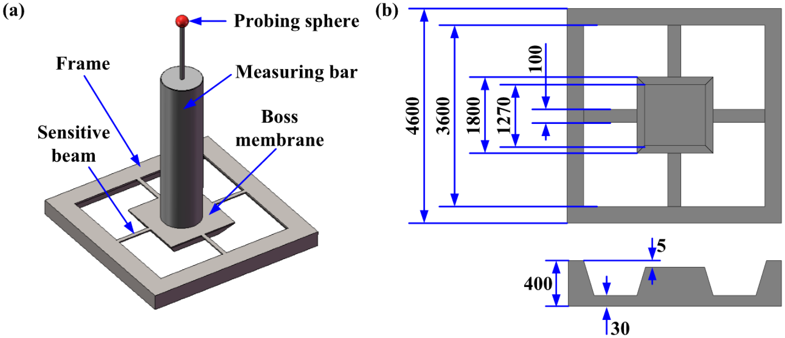
Since the discovery of the piezoresistive effect in silicon by Smith in 1954, it has been widely used in many types of sensors [13]. The 3D microdisplacement sensing system presented in this paper was also based on this phenomenon. The sensing system consisted of a cross-shaped sensitive beam, a 6.8 mm long stylus with a probing sphere of 300 μm diameter, and three Wheatstone bridges, which were connected to a precise data acquisition circuit. The mechanical structure is shown in Figure 1.
2.1. Displacement Detection
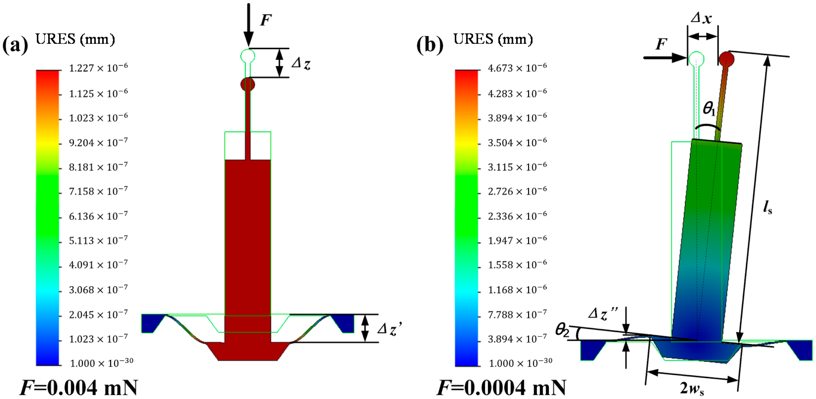
To illustrate the measurement mechanism, a displacement detection model built using SolidWorks is shown in Figure 2. When loaded with an axial or lateral load, the shifting of the probing sphere leads to the shifting of the boss membrane through the measuring bar, which in turn causes the shifting or rotation of the boss membrane. This deforms the sensitive beams and the stresses in the beams are changed. Variations in the stresses can be obtained by measuring the resistance changes in the resistors in the sensitive beams.
The material of the sphere was ruby, and the measuring bar was made of tungsten carbide. The thickness of the boss membrane was 395 μm, which was approximately ten times thicker than the sensitive beam, whose thickness was 30 μm. Thus, the stiffness of the boss membrane was far greater than that of the sensitive beam. This was verified by performing a stress simulation (discussed in Section 2.2). The stylus and boss membrane were connected by epoxy resin. Ruby, tungsten carbide, and epoxy resin have relatively high stiffness values. In other words, the deformation of the displacement transmission system, which consisted of the stylus and boss membrane, could be neglected.
When the sphere is axially displaced by Δz, a shift of Δz′ is generated between the two ends of the sensitive beam, as shown in Figure 2a. Considering the rigidity assumptions for the epoxy resin, stylus, and boss membrane, Δz′ can be viewed as being equal in value to Δz. Figure 2b shows the lateral displacement detection model. The shift of Δz″ between the two ends of the sensitive beam is approximately determined using the expression:
2.2. Stress Simulation
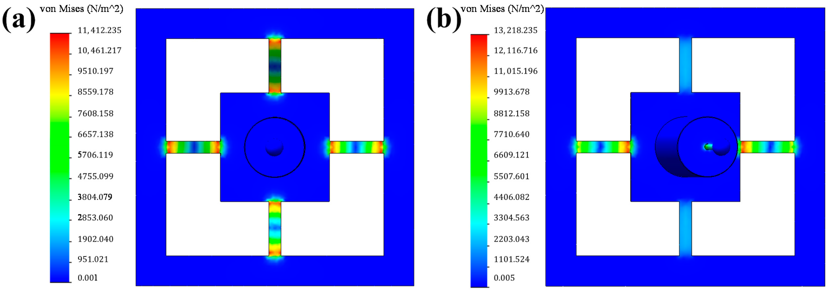
To realize optimal performance, stress simulation was conducted using a finite element method (FEM). Forces of 0.004 and 0.0004 mN were applied in the axial and lateral directions, respectively. The results can be observed in Figure 3. The design parameters of the sensing unit were determined using the FEM. The detailed analysis of the stiffness was similar to that performed in [14].
When a load was placed on the sphere, normal stress was mainly concentrated on the sensitive beam. There was nearly zero stress on the frame and boss membrane. Therefore, the resistors should be distributed at the two ends of each sensitive beam, where there is maximum stress.
2.3. Acquisition Circuit Design
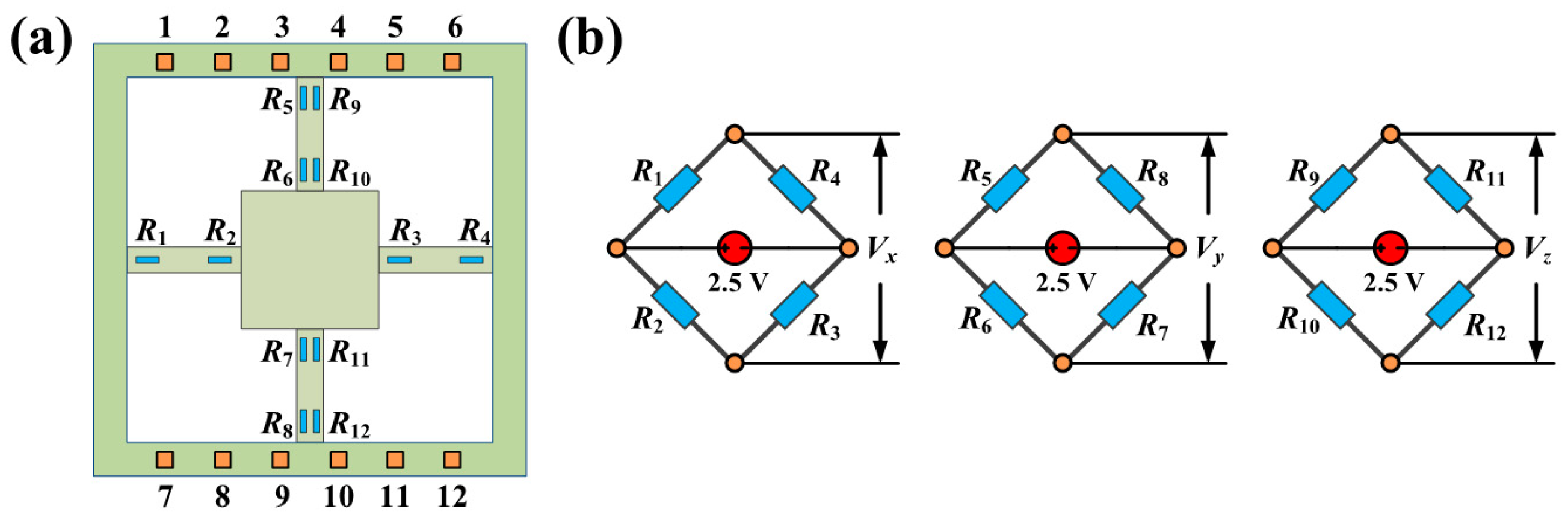
Variations in the stresses in the sensitive beam were detected by the three Wheatstone bridges, each of which consisted of four resistors. The resistors were easily affected by thermal drift. Therefore, the Wheatstone bridge was effective in improving the sensitivity. Figure 4 shows the distribution of the resistors and the connections of each resistor. The outputs of the axial and lateral loads were detected by different bridges. R1–R4 were part of the first Wheatstone bridge, which was used to detect the X-direction stress. R5–R8 were used for Y-direction stress detection, and R9–R12 were used for Z-direction stress detection.
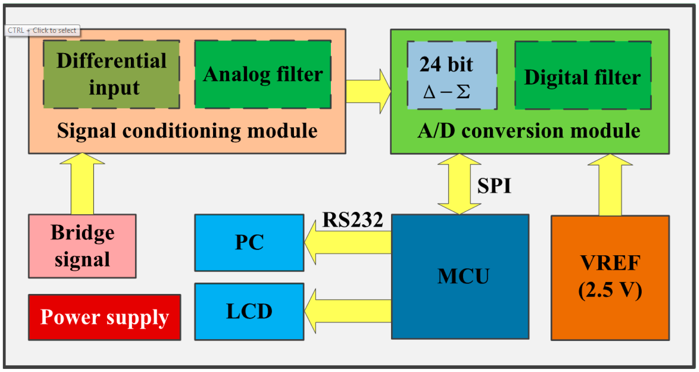
A precise data acquisition system was necessary to achieve a weak voltage signal output in the Wheatstone bridge. The system frame is shown in Figure 5. A precision linear voltage regulator module was designed to ensure stable power supply. The bridge signal was applied difference disposal and analogue filtering before analogue-to-digital conversion. After conversion, digital filtering was performed. ADS1274 was selected as the voltage-to-digital converter, and it has a theoretical resolution of 0.149 μV. The results could be displayed directly on a liquid crystal display or on a software interface by using a personal computer, which made it easy to record and process the results. The full range of the system was ±2.5 V. Owing to the circuit and environmental noise, the acquisition accuracy achieved was 20 μV.
The relative change in the resistance of the resistor as a result of normal stress can be approximately described by the expression:
The output voltage of the Wheatstone bridge Vout is given by:
When using an acquisition accuracy of 20 μV as Vout and an input voltage of 2.5 V as Vin in Equation (3), a ΔR/R value of 8 × 10⁻⁶ is obtained. Subsequently, using this ΔR/R value in Equation (2), a σ1 value of 1.1142 × 10⁴ Pa is obtained. A stress smaller than 1.1142 × 10⁴ Pa was not detected. Therefore, forces of 0.004 and 0.0004 mN were applied in the simulation. The simulation results in Figure 2 show that theoretical resolutions of 1.227 and 4.673 nm were achieved for the axial and lateral directions by using FEM.
3. Fabrication
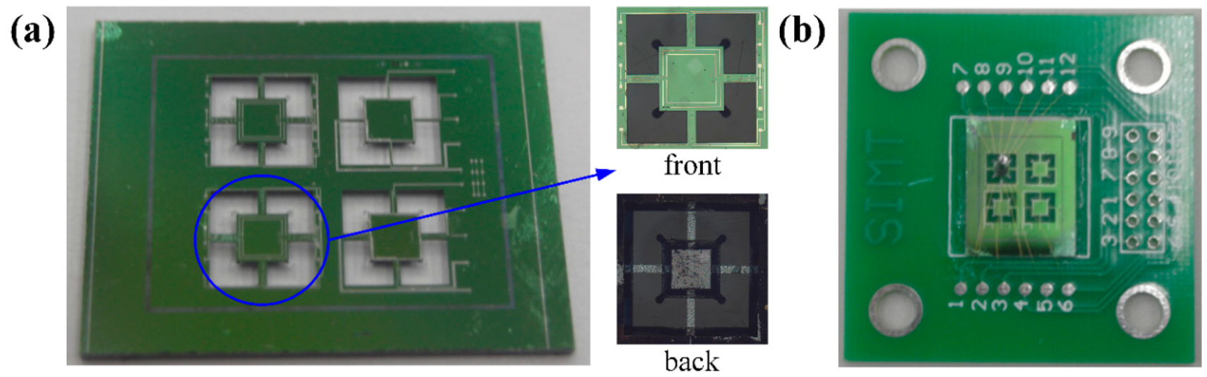
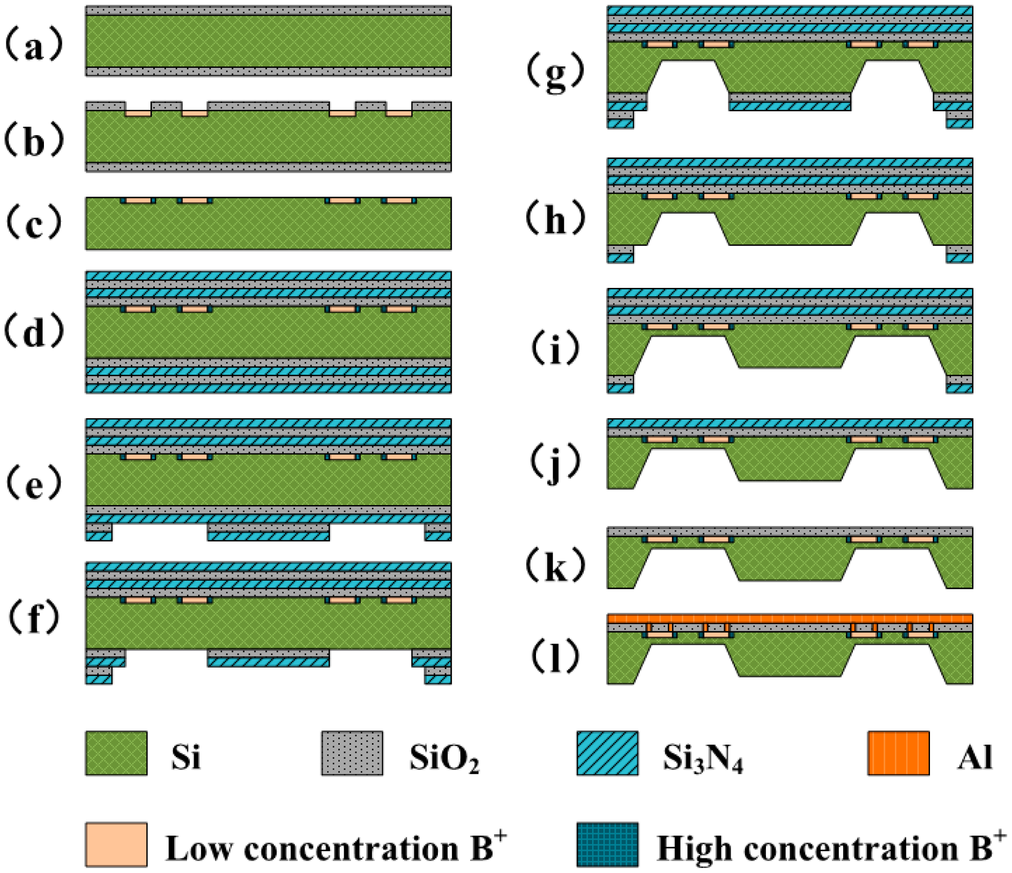
The sensing unit was fabricated using an MEMS bulk-silicon process, which is shown in Figure 6.
Figure 7a shows the manufactured sensing unit, which was fixed on a printed circuit board and connected to the data acquisition circuit through gold wires. The size of each unit was 4.6 mm × 4.6 mm. The assembled sensor is shown in Figure 7b. The value of the fabricated sheet resistor was approximately 5.83 kΩ.
4. Calibration and Analysis
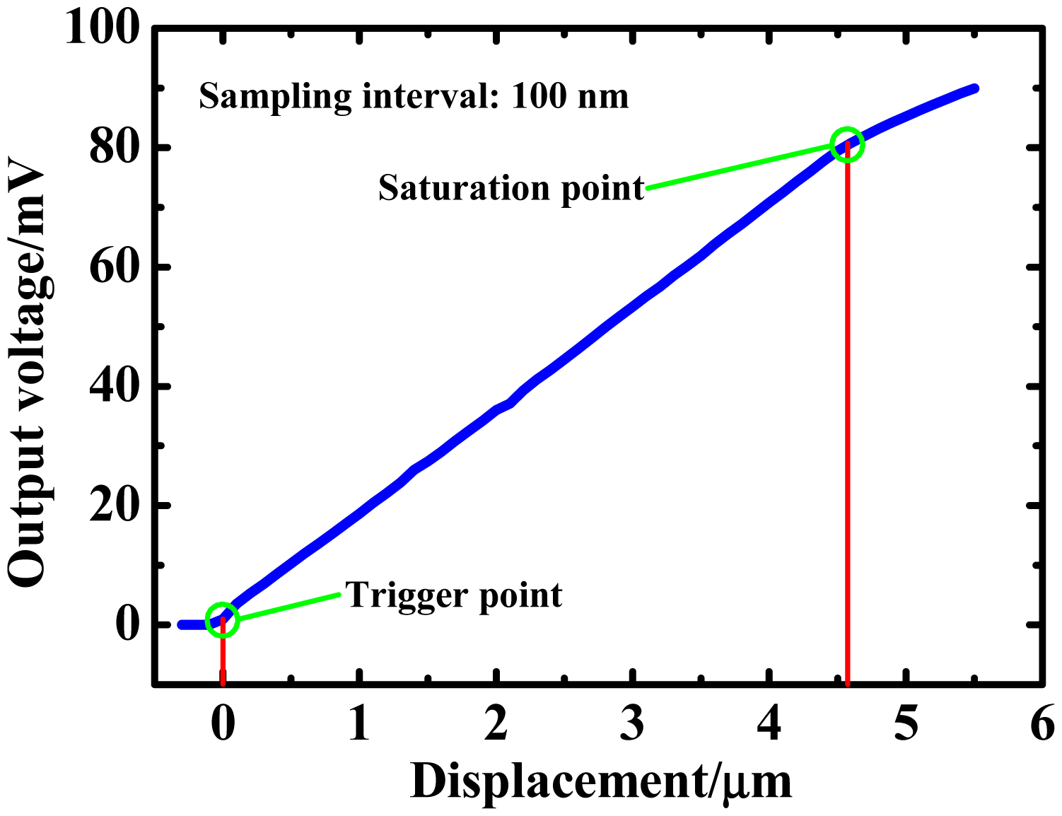
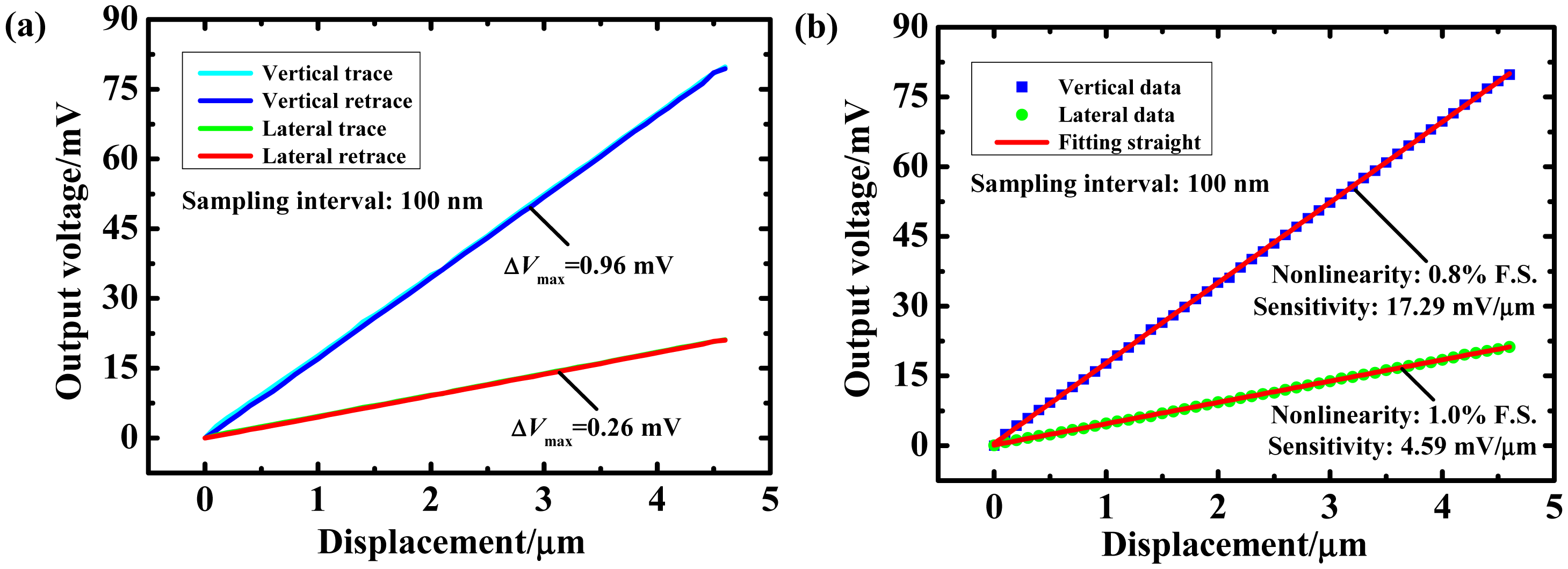
The sensor was calibrated using a nanometre positioning system, which has been described in [15]. The moving stage had a large coarse positioning range of 25 mm × 25 mm × 10 mm, a precise uniaxial positioning range of 12 μm, and an accuracy of 1 nm. A charge-coupled device camera was used as an auxiliary observation tool. The precise uniaxial positioning stage was calibrated by laser interferometer before experiment. The measurement error of the laser interferometer is within 0.7 × 10⁻⁶ L, where L is the measurement range. Figure 8 shows the result of axial range calibration. The sensor had an axial range of 4.6 μm. The saturation point indicates that the boss membrane was in touch with the backboard. The lateral range was not tested because of the risk of fracture. However, from (1), it can be deduced that the lateral range was larger than the axial range.
The hysteresis and linearity were tested to determine the output performance of the sensor (see Figure 9). The axial and lateral hystereses were 0.96 mV and 0.26 mV. Furthermore, the sensor had sensitivity values of 17.29 mV/μm and 4.59 mV/μm during axial and lateral approach, respectively; the nonlinearity values for these approaches were 0.8% full scale (FS) and 1.0% FS, respectively. The linearity was evaluated using linear regression. The R2 values were 0.99993 for axial fitting and 0.99981 for lateral fitting.
Resolution is an important parameter that directly determines the probing precision of a sensor. In the resolution test, the trigger point was set as the starting position. For determining the axial resolution, 50 and 5 nm steps were chosen. Figure 10b shows that the linearity of the straight fitting was 0.98633, which is an acceptable value. For an approaching step less than 5 nm, the linearity of the straight fitting decreased sharply, and data values of the forward and backward points could not be distinguished. Therefore, the axial resolution was regarded as 5 nm. Similarly, the lateral resolution was determined to be 10 nm. Cross-talk was not tested here; it may be mentioned here that cross-talk was observed to be very weak [14].
Additionally, there is another question that should be discussed here. Compared to the triskelion designs by Bos and Claverley, the cross-shape design is over constrained [1,5]. It may have a large effect to the measurement results as the flexure is not full rotational symmetry. However, the decoupling is easier in the cross-shape design. There are two ways to eliminate the influence of non-rotational symmetry. The first way is to calibrate the sensor in x, y and z direction respectively by the nano measuring machine before measurement and apply the obtained input-output curve to calculate the measurement results. The second way is to develop the related algorithm to eliminate the error. The angle of non-rotational symmetry can be calculated by measuring the output voltages of x, y and z axes simultaneously. Then, the calculated angle could be used to correct the measurement results. If the second method is realized, the sensing system can measure displacement in an arbitrary vector in the x-y plane.
5. Conclusions
A 3D microdisplacement sensing system was designed and fabricated using MEMS bulk-silicon technology. A displacement detection model was constructed, and stress distribution was simulated using a FEM. A circuit with three Wheatstone bridges was used to measure the variation in stress and a precise data acquisition system was developed. By calibration, the sensing system was shown to have sensitivity values of 17.29 and 4.59 mV/μm in the axial and lateral directions, respectively; the nonlinearity values in these directions were 0.8% and 1.0% FS, respectively. An axial hysteresis of 0.96 mV and a lateral hysteresis of 0.26 mV were obtained. The results of the resolution test indicated that the sensing system had a 5 nm resolution in the axial direction and a 10 nm resolution in the lateral direction. In future work, aspects such as the probing force, thermal drift, compensations, and repeatability will be investigated. Integration with a nanoscale measuring and positioning platform will be performed by developing an associated hardware interface and software.
Acknowledgments
This work was supported by the National Key Scientific Instrument and Equipment Development Projects of China (No. 2014YQ090709) and State Key Laboratory of Precision Measurement Technology and Instruments.
Author Contributions
In this paper, Junjie Wu designed the experiment and wrote the manuscript. Xin Chen developed the precise data acquisition system and supervised the overall research. Lihua Lei and Xiaoyu Cai conducted the simulations and completed the numerical calculations. Yuan Li proposed the structure of the sensor and designed the fabrication process. Tao Han was responsible for modifying the manuscript and supervising the experiment.
Conflicts of Interest
The authors declare no conflict of interest.
References
- Bos, E.J.C. Aspects of tactile probing on the micro scale. Precis. Eng. 2011, 35, 228–240. [Google Scholar]
- Danzebrink, H.-U.; Dai, G.; Pohlenz, F.; Dziomba, T.; Butefisch, S.; Flugge, J.; Bosse, H. Dimensional nanometrology at PTB. Proceedings of the Instrumentation and Measurement Technology Conference, Graz, Austria, 13–16 May 2012; pp. 898–901.
- Petz, M.; Tutsch, R.; Christoph, R.; Andraes, M.; Hopp, B. Tactile-optical probes for three-dimensional microparts. Measurement 2012, 45, 2288–2298. [Google Scholar]
- Claverley, J.D.; Leach, R.K. A vibrating micro-scale CMM probe for measuring high aspect ratio structures. Microsyst. Technol. 2010, 16, 1507–1512. [Google Scholar]
- Claverley, J.D.; Leach, R.K. Development of a three-dimensional vibrating tactile probe for miniature CMMs. Precis. Eng. 2013, 37, 491–499. [Google Scholar]
- Goj, B.; Dressler, L.; Hoffmann, M. Resonant probing system comprising a high accurate uniaxial nanoprobe and a new evaluation unit. J. Micromech. Microeng. 2013, 23. [Google Scholar] [CrossRef]
- Bütefisch, S.; Büttgenbach, S.; Kleine-Besten, T.; Brand, U. Micromechanical three-axial tactile force sensor for micromaterial characterisation. Microsyst. Technol. 2001, 7, 171–174. [Google Scholar]
- Tan, J.B.; Cui, J.N. Ultraprecision 3D probing system based on spherical capacitive plate. Sens. Actuators A Phys. 2010, 159, 1–6. [Google Scholar]
- Vasarhelyi, G.; Adam, M.; Vazsonyi, E.; Vizvary, Z.; Kis, A.; Barsony, I.; Ducso, C. Characterization of an Integrable Single-Crystalline 3-D Tactile Sensor. IEEE Sens. J. 2006, 6, 928–934. [Google Scholar]
- Vasarhelyi, G.; Fodor, B.; Roska, T. Tactile sensing-processing: Interface-cover geometry and the inverse-elastic problem. Sens. Actuators A Phys. 2007, 140, 8–18. [Google Scholar]
- Adam, M.; Mohacsy, T.; Jonas, P.; Ducso, C.; Vazsonyi, E.; Barsony, I. CMOS integrated tactile sensor array by porous Si bulk micromachining. Sens. Actuators A Phys. 2008, 142, 192–195. [Google Scholar]
- Dao, V.D.; Toshiyuki, T.; Wells, J.; Susumu, S. Silicon piezoresistive six-degree of freedom micro force-moment sensor. Sens. Mater. 2002, 15, 113–135. [Google Scholar]
- Smith, C.S. Piezoresistance effect in germanium and silicon. Phys. Rev. 1954, 94, 42–49. [Google Scholar]
- Lei, L.H.; Deng, L.J.; Fan, G.F.; Cai, X.Y.; Li, Y.; Li, T.B. A 3D micro tactile sensor for dimensional metrology of micro structure with nanometer precision. Measurement 2014, 48, 155–161. [Google Scholar]
- He, M.X.; Liu, R.; Li, Y.; Wang, H.; Lu, X.; Ding, G.F.; Wu, J.J.; Zhang, T.; Zhao, X.L. Tactile probing system based on micro-fabricated capacitive sensor. Sens. Actuators A Phys. 2013, 194, 128–134. [Google Scholar]


© 2014 by the authors; licensee MDPI, Basel, Switzerland. This article is an open access article distributed under the terms and conditions of the Creative Commons Attribution license ( http://creativecommons.org/licenses/by/4.0/).
Share and Cite
Wu, J.; Lei, L.; Chen, X.; Cai, X.; Li, Y.; Han, T. A Three-Dimensional Microdisplacement Sensing System Based on MEMS Bulk-Silicon Technology. Sensors 2014, 14, 20533-20542. https://doi.org/10.3390/s141120533
Wu J, Lei L, Chen X, Cai X, Li Y, Han T. A Three-Dimensional Microdisplacement Sensing System Based on MEMS Bulk-Silicon Technology. Sensors. 2014; 14(11):20533-20542. https://doi.org/10.3390/s141120533
Chicago/Turabian StyleWu, Junjie, Lihua Lei, Xin Chen, Xiaoyu Cai, Yuan Li, and Tao Han. 2014. "A Three-Dimensional Microdisplacement Sensing System Based on MEMS Bulk-Silicon Technology" Sensors 14, no. 11: 20533-20542. https://doi.org/10.3390/s141120533
APA StyleWu, J., Lei, L., Chen, X., Cai, X., Li, Y., & Han, T. (2014). A Three-Dimensional Microdisplacement Sensing System Based on MEMS Bulk-Silicon Technology. Sensors, 14(11), 20533-20542. https://doi.org/10.3390/s141120533