Metallic and Ceramic Thin Film Thermocouples for Gas Turbine Engines

Abstract
: Temperatures of hot section components in today's gas turbine engines reach as high as 1,500 °C, making in situ monitoring of the severe temperature gradients within the engine rather difficult. Therefore, there is a need to develop instrumentation (i.e., thermocouples and strain gauges) for these turbine engines that can survive these harsh environments. Refractory metal and ceramic thin film thermocouples are well suited for this task since they have excellent chemical and electrical stability at high temperatures in oxidizing atmospheres, they are compatible with thermal barrier coatings commonly employed in today's engines, they have greater sensitivity than conventional wire thermocouples, and they are non-invasive to combustion aerodynamics in the engine. Thin film thermocouples based on platinum:palladium and indium oxynitride:indium tin oxynitride as well as their oxide counterparts have been developed for this purpose and have proven to be more stable than conventional type-S and type-K thin film thermocouples. The metallic and ceramic thin film thermocouples described within this paper exhibited remarkable stability and drift rates similar to bulk (wire) thermocouples.1. Introduction
The next generation of gas turbine engines will employ advanced materials, which are designed to handle the harsh environments inside the hot section of these engines [1]. With advances in engine materials comes the need for developing new instrumentation which can handle the higher temperatures, pressures and gas flow to monitor the operating conditions inside the engine during operation. Engine designers must gain an understanding of the operating conditions inside the engine and perform diagnostics in order to ensure it is operating safely and according to the final design parameters. Specifically, improvements such as lighter engine components with superior thermomechanical properties, advanced thermal barrier coatings (TBC) for turbine blades, and higher operating temperatures to improve overall combustion efficiency and reduce harmful emissions are placing greater demands on the instrumentation itself. Therefore, the design and implementation of sensors to monitor operating conditions and perform diagnostics in these engines during testing is becoming an increasingly difficult task.
Many issues arise when attempting to integrate sensors inside gas turbine engines, considering they operate under severe conditions where supersonic nozzle velocities, rotational forces exceeding fifty thousand g, and gas temperatures reaching as high as 1,500 °C in the hot section are present. Conventional wire sensors cannot reliably withstand these conditions due to their relatively large thermal masses and surface profiles that extend beyond the boundary layer of rotating parts, which can affect combustion gas flow patterns and induce mechanical interference with the vibrational modes of rotating parts. As blades and other components get thinner in cross section, efforts have focused on using thin film sensors to replace wire sensors. Thin film sensors do not interfere with gas flow patterns because they have thicknesses on the order of micrometers, well below the boundary layer thickness of instrumented engine component surfaces [2,3]. And since the masses of the sensors are on the order of micrograms, they do not affect the vibrational modes of rotating parts and are not affected by the rotational forces inside the engine [3]. Thin film sensors have much faster signal response times due to lower thermal mass relative to wire sensors [4]. Thin films sensors are directly deposited onto the surface of thermal barrier coatings of stationary and rotating components without the need for high temperature adhesives. As a result, more accurate surface measurements are possible [1,2,5].
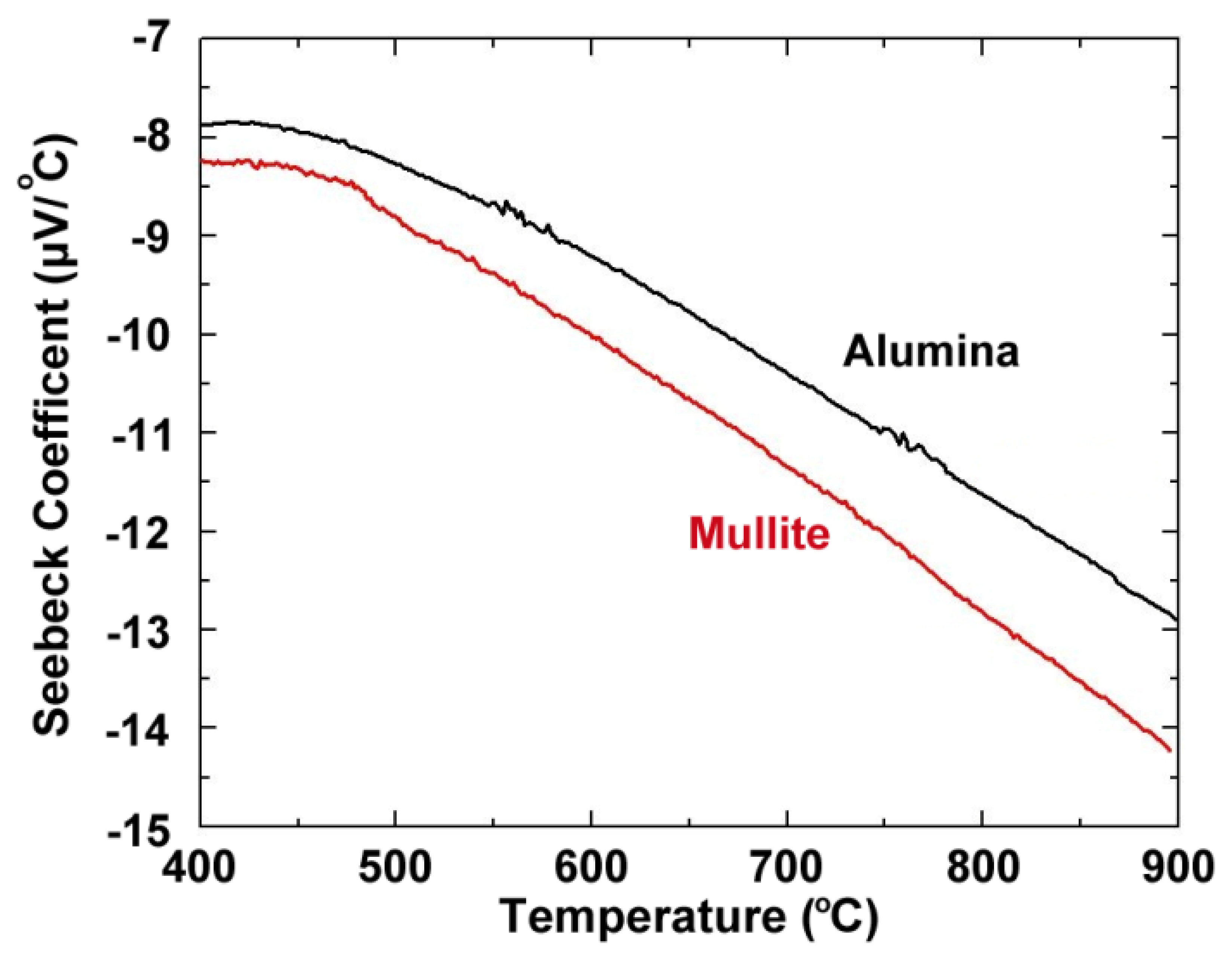
Oxidation in the gas turbine engine environment can cause instability and drift in metallic thin film thermocouples due to the significantly reduced diffusional distances relative to wire thermocouples. For example, in type-S thin film (platinum: 90%-platinum-10% rhodium) thermocouples, selective oxidation of rhodium in the platinum rhodium thermocouple leg forms volatile rhodium oxides at temperatures between 600–800 °C, and can cause degradation of these temperature sensors [6]. The selective oxidation process at high temperature is progressive and time dependent, causing drift in the thermoelectric output by as much as 13.8 °C/h as the platinum-rhodium thermocouple legs undergo both microstructural and compositional changes [2]. Furthermore, the same effect can be seen in type-K (alumel:chromel) thin film thermocouples at substantially lower temperatures. Therefore, more stable metallic thin film thermocouple combinations must be considered, which do not experience detrimental microstructural changes and selective oxidation issues at high temperatures.
Wire thermocouples based on platinum and palladium have been investigated to some extent [7–11], however, investigations of thin film Pt:Pd thermocouples have been somewhat limited. These materials, being elemental metals, avoid many of the issues exhibited by alloy thermo-element materials in high temperature environments, such as selective oxidation seen in type-S thin film thermocouples. The use of thin film Pt:Pd thermocouples on oxidized silicon wafers for radiometric temperature measurements has been considered by Kreider et al. up to 1,050 °C [12,13]. However, due to dewetting issues, these thermocouples could only reliably measure temperatures up to 850 °C and required the use of a titanium bond coat between the silicon wafer and thermocouple elements [12,13].
Additionally, research has focused on ceramic thin film thermocouples as an alternative to metallic thin film thermocouples. Ceramics have high melting temperatures and chemical and electrical stability at high temperatures in oxidizing atmospheres. They also have excellent thermal expansion coefficient compatibility with ceramic thermal barrier coatings applied to the surface of engine components. TiC-TaC thin film thermocouples, while showing promising results up to 1,080 °C, are limited to inert atmospheres or vacuum conditions due to thermo-element degradation in the presence of oxygen at high temperature [14]. Silicides have also been investigated for thin film thermocouples [6]. MoSi2 and TiSi2 proved to be stable in air to 1,200 °C due to a protective silicon oxide layer which grew over the surface of the thermo-elements during thermal cycling. However, this consumes the silicon in the film, changing the chemical composition of the thermo-element, which can lead to drift. To compensate for this loss, a layer of silicon must be deposited beneath the thermo-element. Moreover, silicide- and carbide-based thin film thermocouples have low outputs compared to type-S thin film thermocouples.
Oxides have proven to be more stable as thermo-elements in harsh environment since they contain all the oxygen their structure can accommodate. Indium oxide (In2O3) and indium tin oxide (ITO) are wide band gap semiconductors commonly used in transparent conductor applications, and when In2O3 contains low concentrations of extrinsic dopants (i.e., tin), oxygen vacancies defects are often the primary charge carrier. This defect is defined according to Equation (1):
ITO has improved electrical conductivity over In2O3 because the inclusion of two tin and one oxygen atoms forms a neutral charge carrier site, in addition to self-doping caused by intrinsic defects. Since impurities tend to collect at grain boundaries, the electrical conduction mechanisms in these materials are dictated by the grain boundary area per unit volume. During thermal cycling, these materials undergo sintering which results in changes to the grain boundary area and therefore charge carrier concentration, eventually leading to drift [17]. As previously demonstrated, an all-ceramic thin film thermocouples based on In2O3 and ITO exhibited higher sensitivites than metallic thin film thermocouples with an order of magnitude greater Seebeck coefficient 170 μV/°C at 1,250 °C [18]. However, this same thin film thermocouple had a drift rate of 3.76 °C/h which is an order of magnitude higher than a commercially available metal wire thermocouple.
In this manuscript we review several developments which have recently been demonstrated to improve the performance of thin film thermocouples. Specifically we focus on the development of thin film Pt:Pd and indium oxynitride:indium tin oxynitride (InON:ITON) thin film thermocouples along with their oxide counterparts, which have been deposited onto ceramic substrates via radio frequency sputtering. The thermoelectric properties of Pt:Pd thin film thermocouples were compared to type-S and type-K to determine the benefits of using single element materials rather than alloys for thin film thermocouples in harsh oxidizing environments. The stability of In2O3:ITO thin film thermocouples was improved via nitrogen plasma processing. Due to the sluggish sintering kinetics of nitrides versus oxides, nitrogen plasma processing was used to fabricate InON:ITON thin film thermocouples to improve their stability over the oxide counterparts. The thermoelectric output and drift were measured at temperatures up to 1,100 °C for Pt:Pd and 1,400 °C for InON:ITON thin film. Both exhibited remarkable stability at high temperature in an oxidizing environment. The electrical resistivity and densification as a function of time at temperature of the ceramic thin film thermocouples was measured. Auger electron spectroscopy (AES) was used to characterize the chemical composition of the Pt:Pd metallurgical junctions as a function of depth and to monitor the extent of oxidation. The microstructure of the thin film thermocouples were examined using scanning electron microscopy (SEM).
2. Experimental Section
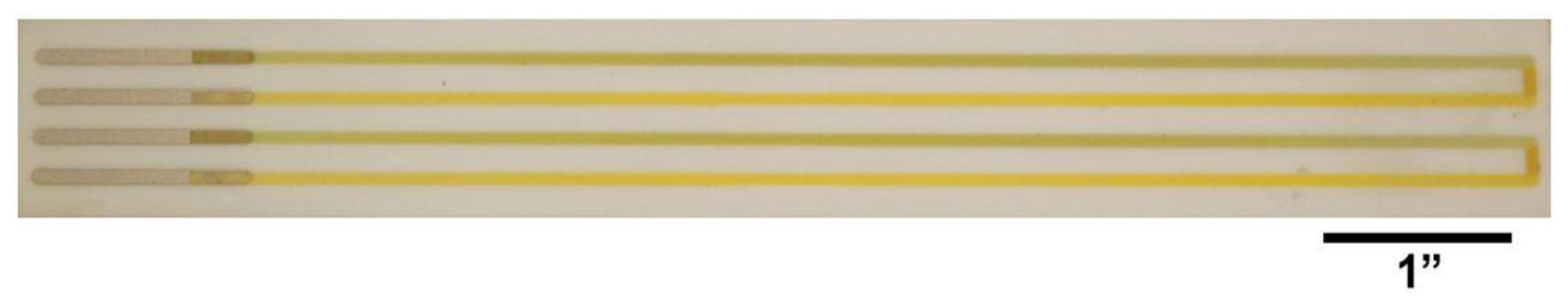
All thin film thermocouples were deposited onto either alumina or mullite ceramic substrates (CoorsTek Inc., Golden, CO, USA) which measured 190 mm × 25 mm × 2 mm. Each substrate was cleaned with acetone, methanol, and deionized water. A dry film negative photoresist (MX 5050™, DuPont™, Wilmington, DE, USA) was soft-baked to the surface of the substrates and bond pad patterns were transferred to the photoresist using a 350 nm wavelength ultraviolet light Optical Associates, Inc. aligner (San Jose, CA, USA) to expose the resist. All optimized sputtering parameters for the various films used in this study are shown in Table 1 and all films were deposited either in a model 8667 or 822 Materials Research Corporation (now owned by a subsidiary of Sony Corporation of North America, Praxair, Danbury, CT, USA) sputtering system. An initial photolithography step was performed prior to depositing the thermocouple elements to pattern platinum bond pads. A second photolithography step transferred a thin film thermocouple leg pattern to the resist using the same ultraviolet light exposure. Windows of the desired patterns were developed in the film after exposure and the first thin film thermocouple leg was sputtered. The second photolithographic step was repeated to fabricate the second thin film thermocouple leg. Films were deposited in pure argon except for the oxynitride materials which were sputtered in a combination of argon and nitrogen, where the total gas pressure was 1.2 or 1.33 Pa for metals and ceramics, respectively. A background pressure of 2.7 × 10⁻⁴ Pa was achieved in the sputtering chamber prior to sputtering, the stage (work piece) was maintained at temperatures below 100 °C using water-cooling, and the targets were pre-sputtered onto shutters for 10 min to remove surface contamination and release adsorbed moisture. Metal thin film thermocouples were anywhere from 1–5 μm thick and ceramic thin film thermocouples were 10–12 μm thick, depending on the material. Fully fabricated thin film thermocouples on a ceramic substrate are shown in Figure 1.
All thin films were annealed in nitrogen for 5 h at 500 °C to remove point defects, including trapped argon, and densify the films. A second anneal was performed in air for 2 h at 1,200 °C to ceramic thin film thermocouples only. This was intended to expose the entire thermocouple to a temperature over 1,000 °C prior to testing to prevent the hot and cold junction from sintering and oxidizing unevenly when applying the thermal gradient induced during testing. Uneven heating creates inhomogeneities in the microstructure and extent of sintering, which leads to drift and eventually device failure. The annealing step prevents this from occurring and stabilizes each thin film thermocouples for longer duration use.
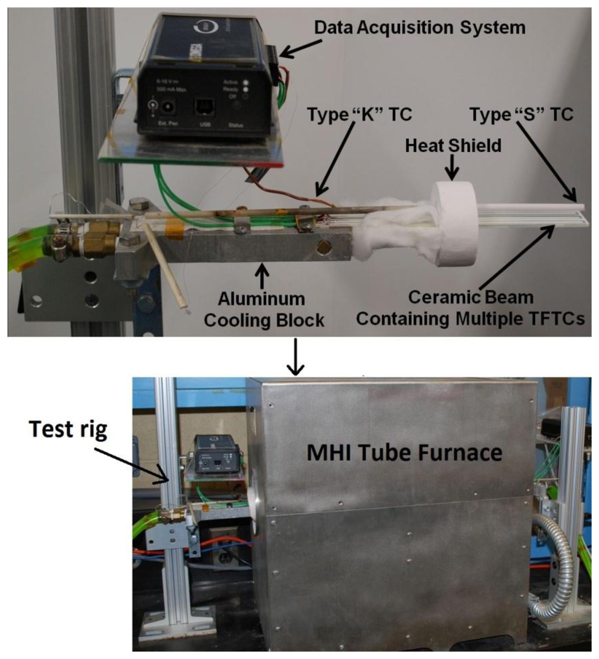
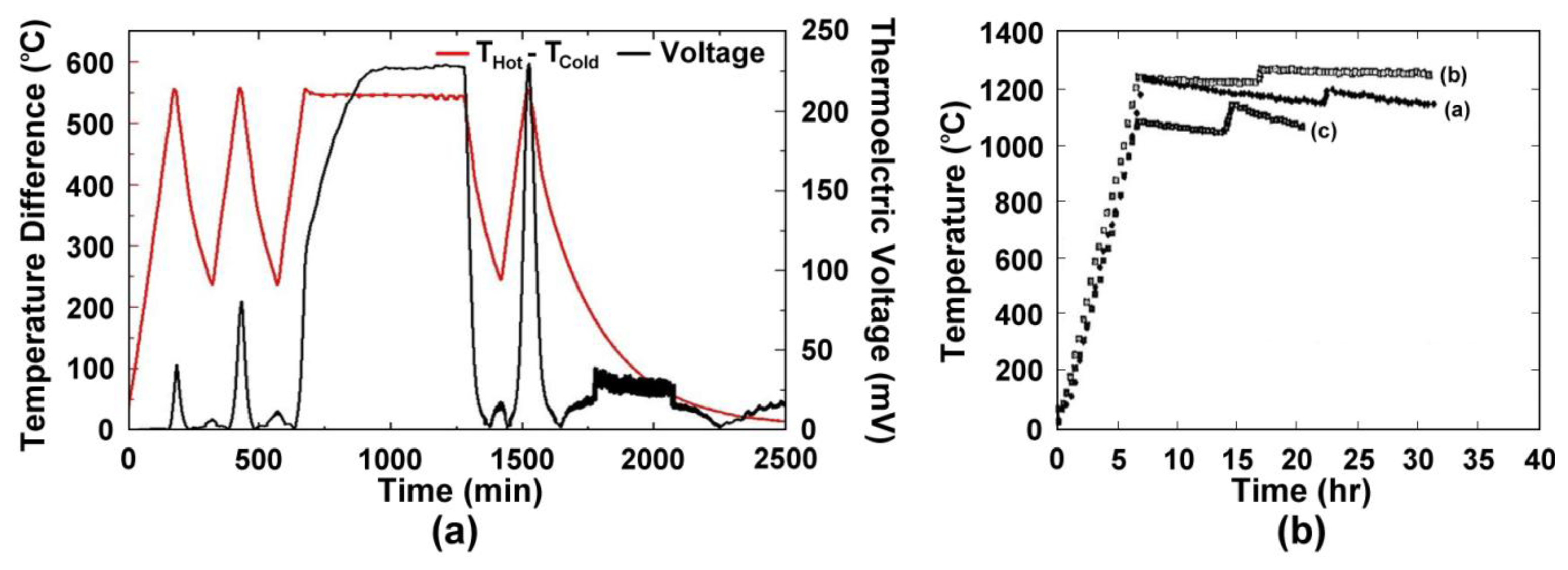
The thermoelectric output of each thin film thermocouple was measured as a function of time and temperature by placing the hot junction in the hot zone of a tube furnace and attaching the cold junction to an aluminum chill block outside the furnace. In this way, a temperature difference was applied along the length of the beam and the cold junction was maintained at or below 100 °C using chilled water or ethylene glycol. Since the temperature of the cold junction could not be maintained at a constant value due to cooling limitations, a wire type-K thermocouple was used to measure the temperature on the cold side of the ceramic substrate. The test apparatus used for all experiments is shown in Figure 2. The thermal cycling protocol is as follows: heat from room temperature at 4 °C/min to desired peak temperature, hold for 10 min, cool from peak temperature to 250 °C at 4 °C/min and hold for 6 min, repeat first cycle from 250 °C to peak temperature and back at the same rate, heat to peak temperature and hold for 10 h, cool to 250 °C and hold for 6 min, repeat second cycle, and cool to room temperature. Pt:Pd thin film thermocouples were thermally cycled in air to 900 °C for several cycles to determine the thermoelectric voltage and drift rate over a 10 h period. In2O3:ITO-based thermocouples were thermally cycled to 1,200 °C for several cycles and their long-term stability was obtained by holding at a temperature difference of 1,200 °C for 200 h. The temperature difference was continuously monitored using type-K (cold junction) and type-S (hot junction) wire thermocouples and copper extension wires were attached to the platinum bond pads of the Pt:Pd thin film thermocouples using a silver paste to acquire the voltage signals. All copper wires and wire thermocouples were connected to an Personal Daq 54 USB data acquisition system (Measurement Computing, Norton, MA, USA) with PDaq View Plus© software recording the temperature and voltage signals. The Seebeck coefficient and drift rates of the thin film thermocouples were determined as a function of hot/cold junction temperature and time, respectively. The Seebeck coefficient defined in this study is given by Equation (2):
To better understand the electrical properties of the semiconducting oxide- and oxynitride-based thermocouples, the resistivity was determined as a function of temperature using the van der Pauw method as a function of temperature and is described by Equation (3):
where k is Boltzmann's constant, T is the absolute temperature, σ0 is a pre-exponential factor, σ is the electrical conductivity, and ΔEa is the activation energy which is the energy gap between the conduction band edge and the Fermi level. The sintering and growth kinetics of In2O3 films sputtered in different argon, oxygen and nitrogen partial pressures deposited on highly polished alumina wafers was measured using a Dektak IIA (currently Bruker, Camarillo, CA, USA) surface profilometer to determine the change in thickness of films as a function of time at temperature. Auger electron spectroscopy (AES) depth profiles were used to determine the chemical composition of the metallurgical junction and identify any oxidation formed on the platinum and palladium thermocouple legs. AES was performed using a 5500 Multi-Technique Surface Analyzer (Perkin Elmer, Waltham, MA, USA). A background pressure of 6.0 × 10⁻⁷ Pa was established and a 1 × 1 mm area on the surface of each thin film thermocouple was sputter cleaned for 10 s prior to acquiring each depth profile. SEM was performed on the same films to analyze the microstructure after thermal cycling using a JSM-5900LV SEM (JEOL, Peabody, MA, USA) and a 20 kV accelerating voltage. SEM micrographs of oxide- and oxynitride-based thermocouple cross-sections and film surfaces were also taken using the same equipment and parameters. Additionally, the oxide and oxynitride films were deposited onto sapphire substrates and grazing incidence X-ray diffraction (GI-XRD) using a CuKα radiation source was used to identify the phases present in the thin films.
3. Results and Discussion
3.1. Thermoelectric Measurements
3.1.1. Type-K and Type-S Thin Film Thermocouples
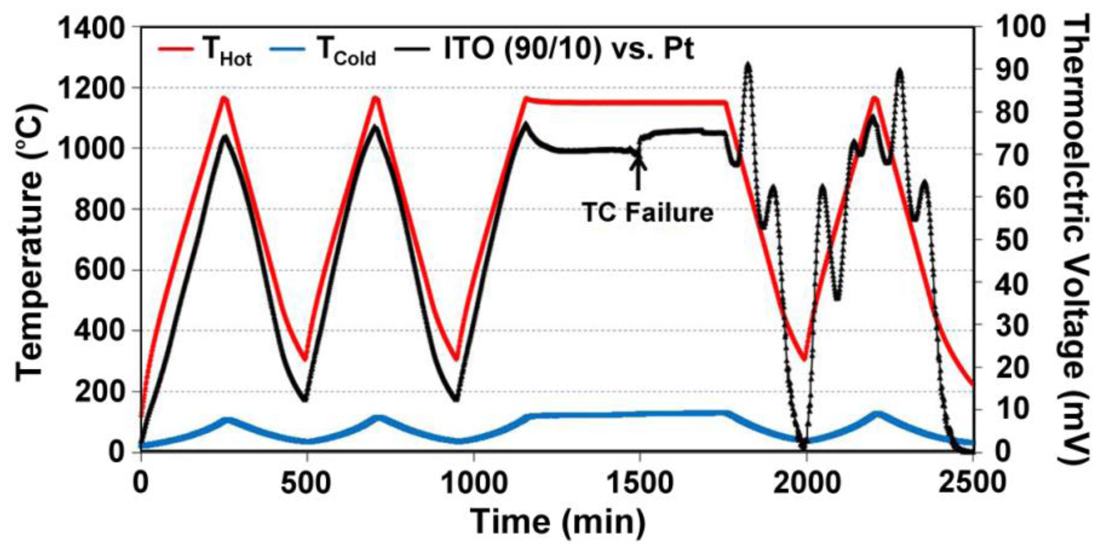
Wire thermocouples based on alumel:chromel (type-K) and platinum:platinum-10% rhodium (type-S) are commonly used for high temperature measurement in the 500–1,500 °C range. However, many other issues arise for thin films of these materials that reduce their performance. Figure 3 shows the time, temperature, thermoelectric response of type-K (a) and type-S (b) thin film thermocouples studied in previous work [2]. The type-K thin film thermocouple shown in Figure 3a was unstable even at low temperatures. Due to the much shorter diffusional length of oxygen through the film versus a wire (micrometers versus millimeters) and oxidation of the films during thermal cycling, drift was prominent and the device failed to perform stably over long periods of time. The increase in peak thermoelectric voltage is attributed to microstructural changes in the film, such as oxidation, as well as progressive dewetting of the film and evaporation. Figure 3b shows three different type-S thin film thermocouples, which were subjected to different thermal cycling ambient and temperature differences from a previous study [2]. The instability of these thermocouples made them unsuitable for use in harsh high temperature environments and therefore thin film thermocouples based on refractory metals and ceramics were investigated.
3.1.2. Platinum: Palladium Thin Film Thermocouples
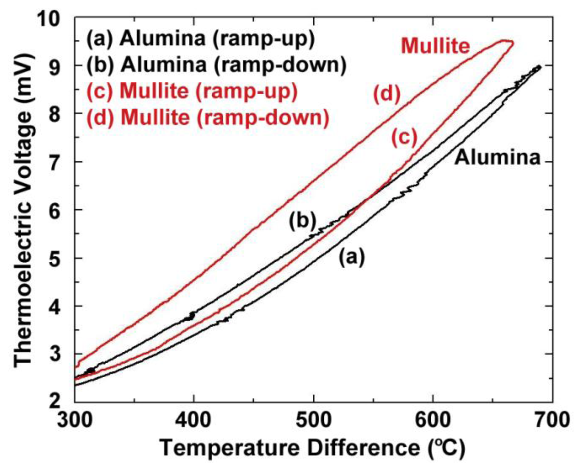
Figure 4 shows the thermoelectric response of several platinum:palladium thin film thermocouples where a temperature difference as large as 750 °C was established along the length of the ceramic substrates and a peak temperature of 900 °C was achieved. The maximum thermoelectric voltage at peak temperature was 9.00 mV on alumina substrates and 9.52 mV on mullite substrates. This thermoelectric response was comparable to a conventional type-S wire thermocouple [19]. The Pt:Pd thin film thermocouples were more stable than both type-K and type-S over many thermal cycles with only slight decreases in peak thermoelectric voltage with each ramp in temperature due to microstructural changes such as grain growth, pore growth, and dewetting of the film, which was later confirmed by SEM imaging [16]. The hysteresis of these thin film thermocouples was smaller than that seen for type-K and type-S, where for the type-K it was much harder to measure due to significant instability in the thermoelectric response. Figure 5 shows the hysteresis for the Pt:Pd thin film thermocouples upon heating and cooling to 900 °C. In an ideal case, the thermoelectric voltage would be identical on the ramp up and ramp down. However, these thin film thermocouples had low hysteresis especially when compared to the metallic thin film thermocouples they were compared against. Here, the thin film thermocouples on mullite exhibited greater hysteresis than those formed on alumina.
The Seebeck coefficient of metal thermocouples is described by Equation (4):
3.1.3. Ceramic Oxide and Oxynitride Thin Film Thermocouples
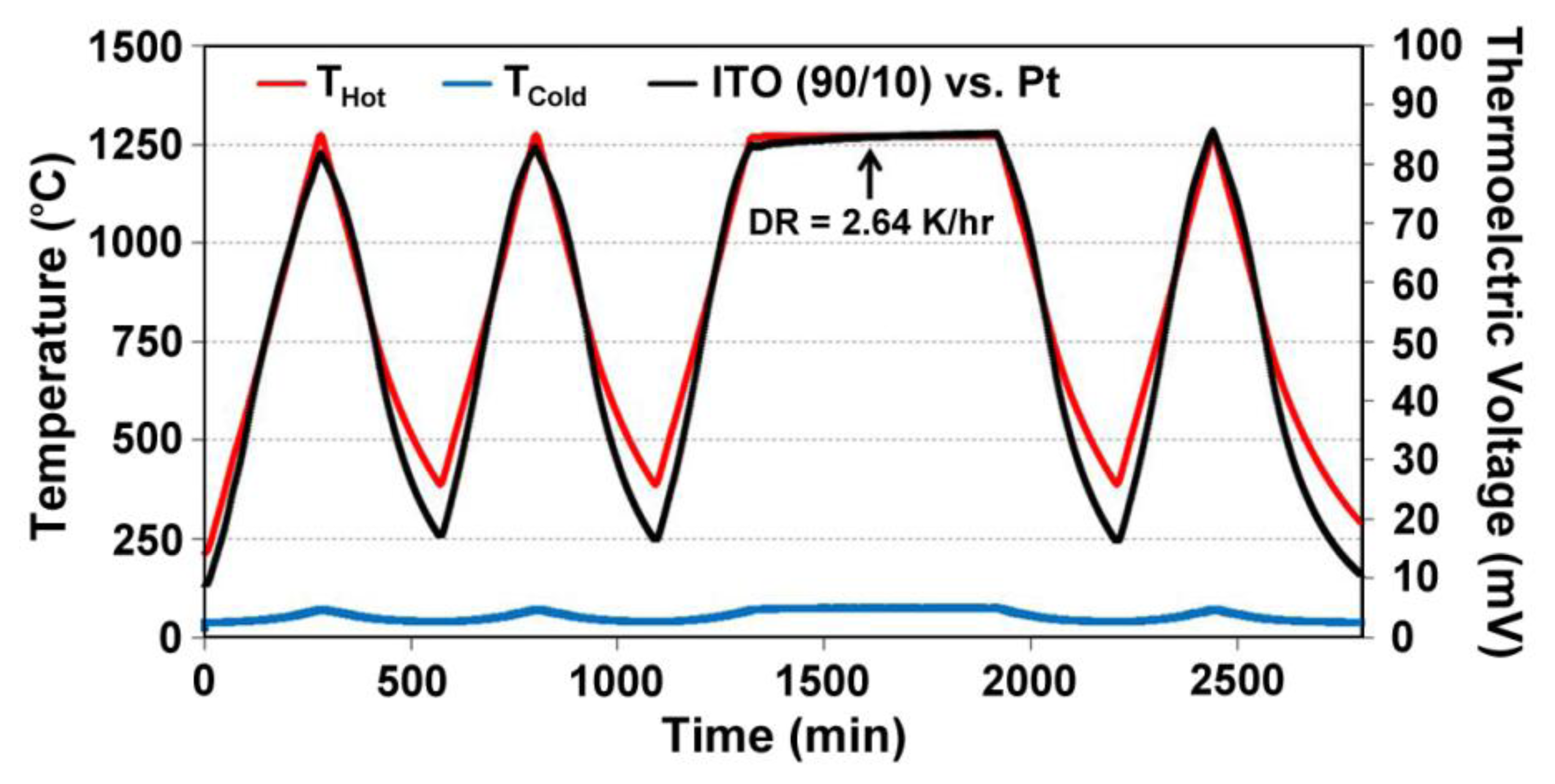
Unbalanced compensation of oxygen vacancies in In2O3-based thin film thermocouples leads to inhomogeneities between the cold and hot junction microstructures, which lead to drift and eventually device failure during high temperature cycling. Data from a Pt:ITO 90/10 thin film thermocouple, which was not air-annealed prior to testing is shown in Figure 8. ITO was tested against a platinum reference leg to measure its true response. During the soak period there is noticeable drift to a point where the signals become unstable at a constant temperature difference and eventually become noisy and incoherent. At this point, there was enough difference in the microstructures and carrier concentration in the semiconductors used to form the hot and cold junction to cause the device to perform unstably. Therefore, all ceramic thin film thermocouples in this study were air annealed prior to testing to avoid premature device failure. Figure 9 shows an equivalent Pt:ITO thin film thermocouple which was annealed in air prior to testing. Note the direct improvement in signal drift and device durability over the same testing period.
The effects of reactive sputtering on the thermoelectric output of In2O3 was investigated and the Seebeck coefficient of each is shown in Figure 10. These thermocouples were tested relative to platinum reference electrodes to measure the true output and it was found that the films prepared in pure argon and in oxygen rich plasmas had larger magnitude Seebeck coefficients than those deposited in nitrogen-rich plasmas. For non-degenerate semiconductors, such as In2O3, a decrease in the carrier concentration increases the magnitude of the Seebeck coefficient. The Seebeck coefficient of non-degenerate semiconductors is described by Equation (7):
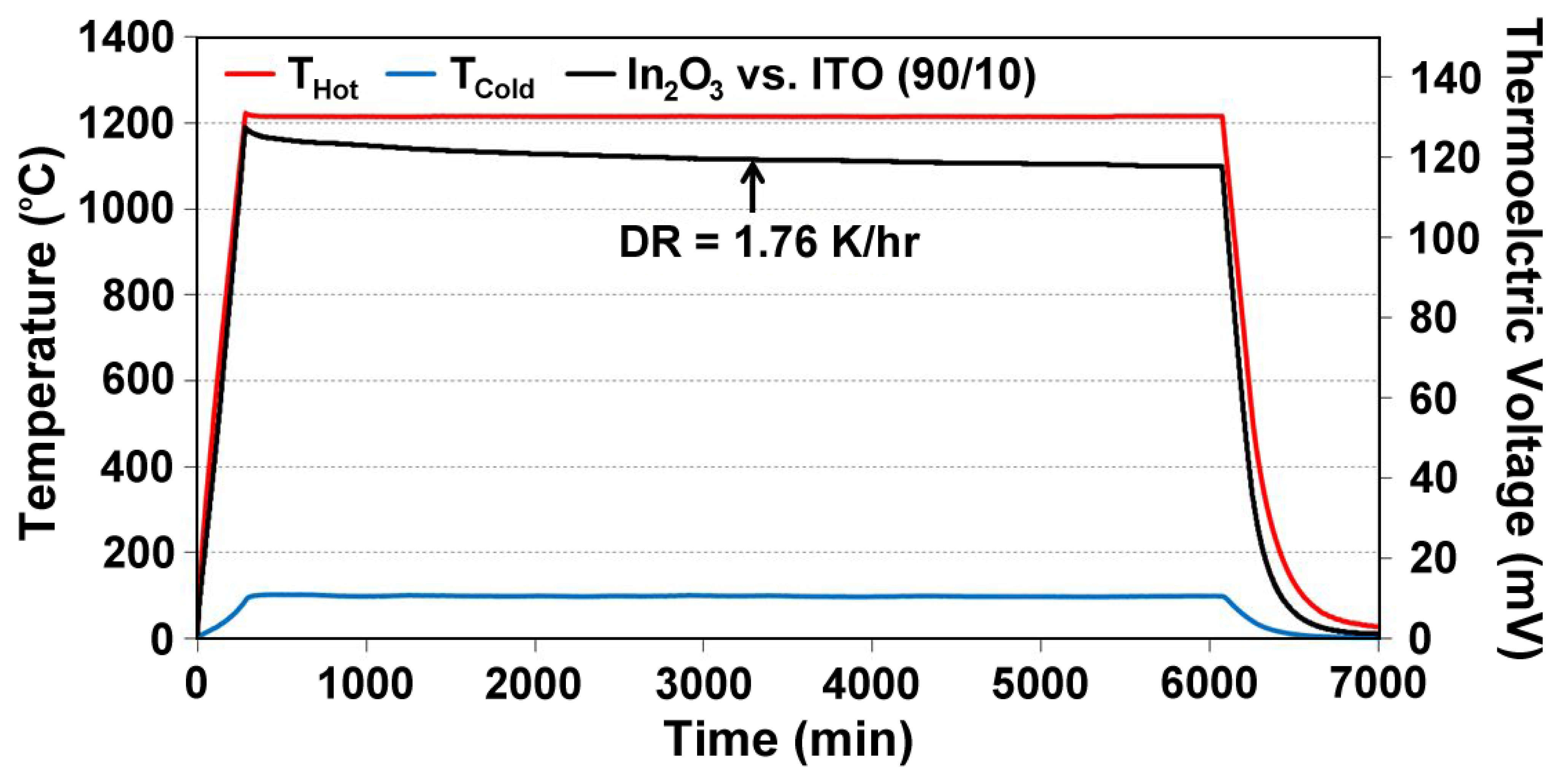
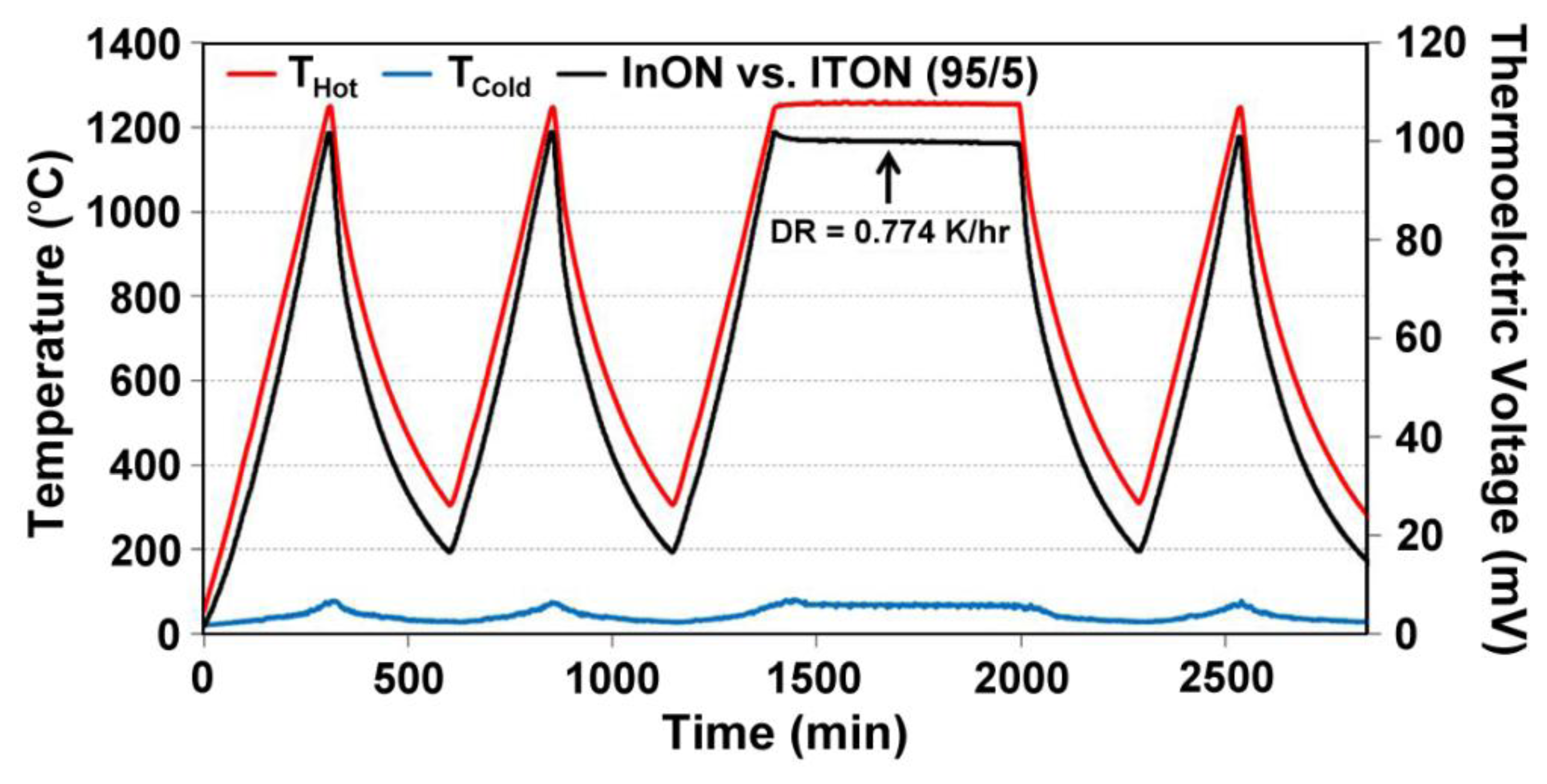
Parameters for equations relating the temperature difference to the thermoelectric voltage of the thin film thermocouples tested in this study, as well as their drift rates, are presented in Table 2. For both metallic and ceramic thin film thermocouples, a cubic polynomial was chosen as the model of best fit based on the hysteresis curves in Figures 5 and 15. Additionally, Table 3 presents the drift rates for the thin film thermocouples tested. Note the order of magnitude reduction in drift rates for Pt:Pd versus type-S and InON:ITON versus In2O3:ITO thin film thermocouples. For comparison, a 0.5 mm diameter type K wire thermocouple had a drift rate of 0.18 K/h at a hot junction temperature of 1,100 °C [15]. While the oxynitride ceramic thermocouples were not able to achieve drift rates lower than their metal wire counterparts, the stability was reduced to the same order of magnitude while providing the performance and versatility of thin film instrumentation.
3.2. Electrical Resistivity of Ceramic Thin Film Thermocouples
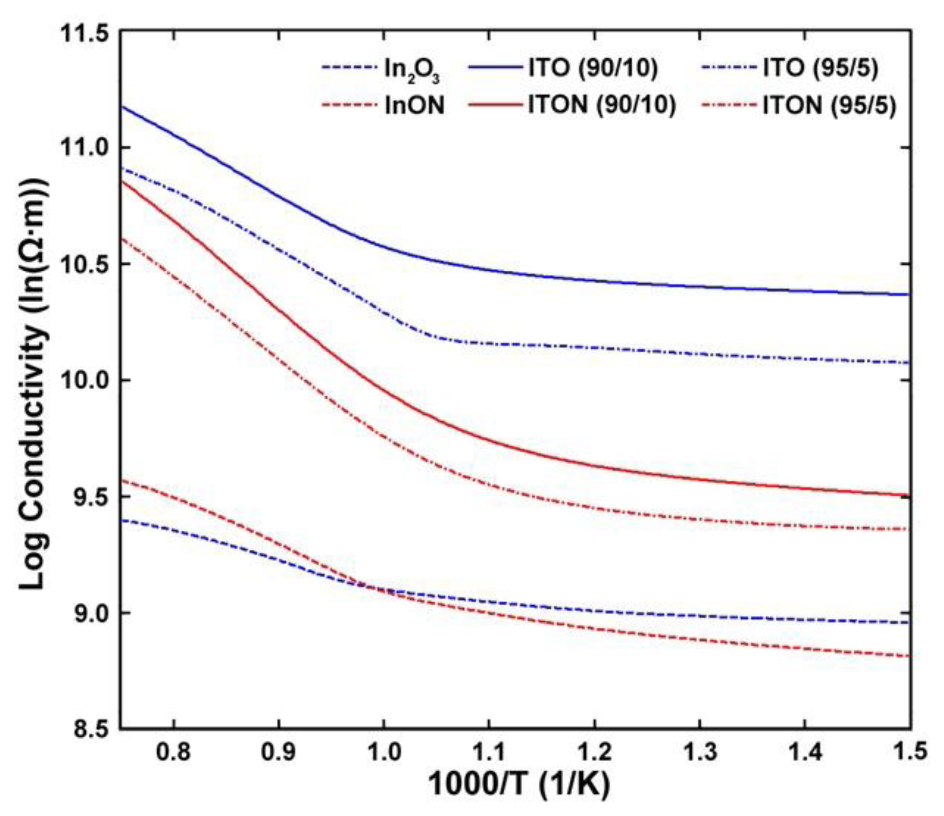
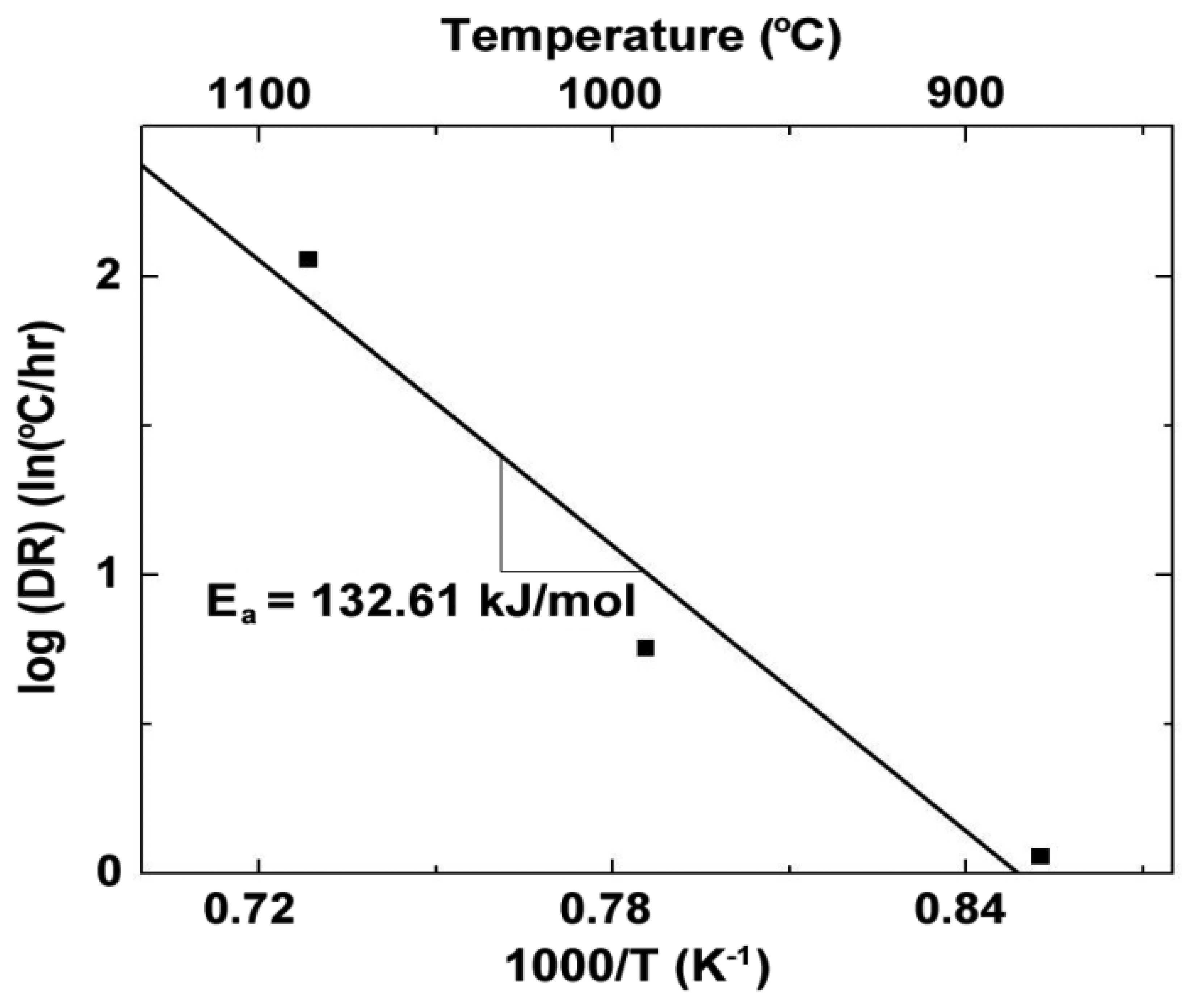
Arrhenius plots showing the electrical conductivity and activation energy of both argon and nitrogen processed In2O3 and ITO films are displayed in Figure 16. The activation energies corresponding to temperatures above and below the observed transition temperature are listed in Table 4. The oxynitride thin films had anywhere from 40–60% higher activation energies than their oxide counterparts. This indicates that nitrogen was present in the bulk film because it acts as a valence band acceptor in oxide semiconductors which results in a reduction of the Fermi energy, explaining the shift in activation energy. In all cases, the oxynitride thin films were more resistive at room temperature than the oxide thin films.
3.3. Chemical Analysis, Crystallography and Microstructure
3.3.1. Platinum:Palladium Thin Film Thermocouples
AES was used to determine the chemical composition of the platinum and palladium thin films. Palladium contained no oxidation and on platinum it was limited to less than 1 nm on the surface. Oxygen was detected at small atomic percentages but was sourced from exposed ceramic substrate where the thin film had dewetted as a result of thermal cycling. Oxygen solubility in platinum and palladium is very low (0.035 atomic percent in palladium at 4.0 × 10⁴ Pa oxygen partial pressure and 850–900 °C) so it was not expected that the oxygen detected was from platinum and palladium oxides [23]. Above 500 °C, instead of forming a surface oxide, platinum evaporates as platinum metal or PtO2 and the extent to which this occurs is proportional to temperature and oxygen partial pressure [24,25]. Often, PtO2 decomposes and redeposits platinum metal on the surface of the film so that the overall material loss is minimal when compared to other noble metals [24]. Therefore, the oxygen detected at thicknesses less than 1 nm on the surface of platinum were likely from oxides which formed during cooling from elevated temperature and formed below 500 °C. No oxidation was found on the surface of the palladium thin films which is expected because it is much more likely that palladium will evaporate as a metal or as one of its volatile oxide, such as PdO, at high temperature [24]. Surface oxides formed on palladium decompose at temperature greater than 850 °C, and above 1,000 °C, the vapor pressure of palladium metal exceeds PdO at atmospheric pressure, so material loss from the thin film is likely palladium metal [24,25]. Depth profiling via AES revealed that platinum and palladium interdiffused at the metallurgical junction to form a complete solid solution of 90/10 atomic percent Pt/Pd on alumina and 78/22 atomic percent Pt/Pd on mullite, which is expected based on the phase diagram for this system [26].
The microstructures of platinum and palladium thin films on both alumina and mullite were found to exhibit dewetting and faceting after thermal cycling. This was evident due to exposed substrate through area in which the film once covered as well as recrystallization from the faceting of pore edges at grain boundaries in particular. Palladium films contained larger pore sizes and grains than platinum which is due to its lower melting temperature and four order of magnitude higher surface recession rate than platinum [24]. The micrographs of each films are presented in Figure 17 where it is seen that each film exhibited dewetting, the palladium to a larger extent than platinum. All films remained contiguous after thermal cycling despite dewetting. The topography of the films on the mullite substrate appears much different than those on alumina because of the difference in surface roughness of each substrate. The mullite, being rougher than the alumina, induced more residual stress and surface energy in the thin films which increased the driving force for dewetting. The microstructures appear similar to those formed via the vapor phase transport mechanism in which continuous faceting of the metal film resulted from the dewetting process [2]. Faceted striations in the thin films, which is indicative of the vapor phase transport, were imaged at higher magnifications in Figure 18. Dewetting occurred at the metallurgical junction but to a lesser extent than the individual platinum and palladium legs since the junction was thicker and faceted striations were also observed. Delamination at the overlap of the metallurgical junction with the palladium leg was a result of the dewetting process in which the palladium leg had receded from the junction. While the thermocouple still functioned properly despite the recession of the film, delamination and dewetting ultimately lead to device failure where, in the limit, the platinum and palladium films would debond completely, most likely at the junction/thermocouple leg interface.
3.3.2. Ceramic Oxide and Oxynitride Thin Film Thermocouples
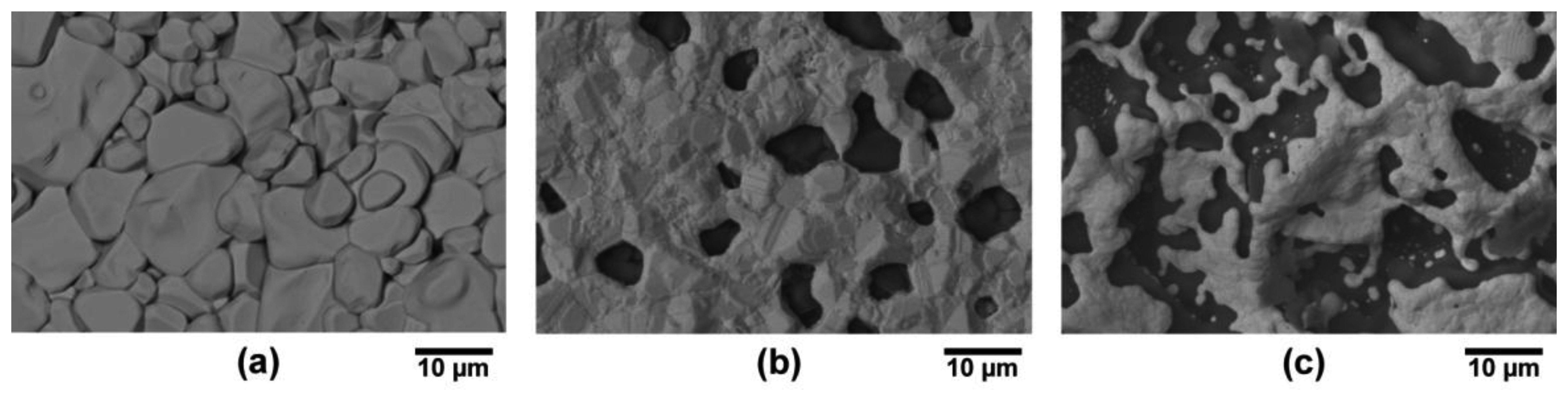
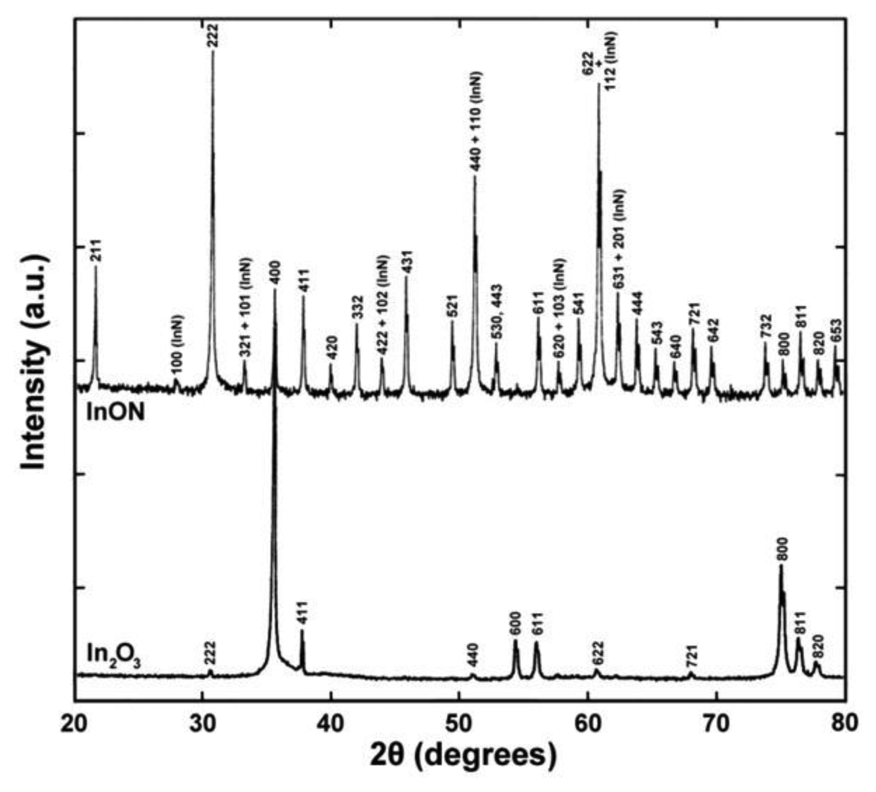
The microstructure of thermally cycled InON and In2O3 films are shown in Figure 19 where the InON film contained submicrometer pores in cross-section which were capped with a densified oxynitride layer (Figure 19a). A dissimilar microstructure was seen for the densified Ar processed film (Figure 19b) which contained very little porosity and no densified layer. The appearance of faceted particles over a network of submicrometer grains (Figure 20) was only observed for InON films but not for any tin doped films (ITON) or In2O3. This is believed to be the result of a vaporization-condensation mechanism where InON growth was driven by the appearance of unstable phases of indium oxides at temperatures greater than 1,200 °C (In2O3 → In2O(g) + O2 and In2O3 → 2InO(g) + 1/2O2) [27] and oxygen-partial pressures [28]. Oxide and oxynitride films were deposited onto sapphire substrates and their x-ray diffraction patterns are shown in Figure 21. The In2O3 films were oriented based on a well defined (400) peak and the films processed in nitrogen contained peaks corresponding to both In2O3 and InN phases. A slight increase in the lattice spacing was observed in the InON films relative to the In2O3 films with an increase from 2.530 Å to 2.546 Å for the (400) peak. This has been found previously in ITON and other oxynitride materials and is an indication that nitrogen is retained in the film and the densified surface layer [18,29].
Kim et al. found that rapid densification of film surface grains constrains sintering in the bulk of the film, which suggests that nitrogen incorporated into the oxynitride film during deposition was metastably retained in pores and at grain boundaries due to the formation of the densified surface layer [30]. When the oxynitride films were thermally cycled, the slower sintering kinetics of nitrides relative to oxides resulted in pore growth and expansion in the bulk film as well as inhibited oxygen diffusion due to the densified surface layer. This phenomenon has been previously discovered in sintering of submicron silicon powder, MgO, ZnO, and SnO2 [31,32] and constrained volume shrinkage ([V0–V]/V0) due to this phenomenon has previously been investigated as a function of time and temperature [30]. Figure 22 shows the isothermal constrained volume shrinkage of In2O3 and InON films as a function of time at 1,300 °C in air. In2O3 prepared in Ar/O2 plasma was found to densify during the first hour at temperature followed by sublimation, and no significant change in thickness was observed for the argon processed film. InON experienced a 12% increase in volume after 2 h at 1,300 °C, which is indicative of the observed pore growth [31].
4. Conclusions and Outlook
Thin film instrumentation based on metallic and ceramic constituents have been developed for use in gas turbine engine applications to replace type-S, type K and other metallic thin film thermocouples, which suffer from oxidation and degradation during thermal cycling. Pt:Pd thin film thermocouples were more stable than type-S and type-K at temperatures over 1,000 °C. Additionally, by incorporating excess nitrogen into the ceramic films via reactive sputtering indium oxynitride-based thin film thermocouples were fabricated and outperformed their oxide counterparts in terms of drift rate and hysteresis. It was confirmed that metastable nitrogen was retained in the films, and due to the slow sintering kinetics of nitrides, the grain boundaries were stabilized and the formation of a densified surface layer on the film was also observed, which inhibited oxygen diffusion during thermal cycling. While not all thin film thermocouples outperformed their wire counterparts, many of the thin film thermocouples exhibited drift rates on the same order as wire thermocouples operating in the same temperature range. The ceramic-based thin film thermocouples exhibited an order of magnitude improvement in thermoelectric power relative to metal-based thin film thermocouples. Dewetting and related microstructural changes in the platinum and palladium thin films could be further inhibited by depositing thicker films (about 5–10 μm). Overall, the metallic and ceramic thin film thermocouples investigated here showed considerable promise as temperature sensors for harsh environments, such as the gas turbine engine hot section, due to their remarkable stability relative to currently available commercial instrumentation.
Acknowledgments
The authors would like to thank the NASA Glen Research Center, Cleveland, Ohio for the support of this work under NASA Grant NNX07AB83A (Aircraft Ageing and Durability Project).
Conflict of Interest
The authors declare no conflict of interest.
References
- Wrbanek, J.D.; Fralick, G.C.; Zhu, D. Ceramic thin film thermocouples for SiC-based ceramic matrix composites. Thin Solid Film 2012, 520, 5801–5806. [Google Scholar]
- Aniolek, G.E.; Gregory, O.J. Thin film thermocouples for advanced ceramic gas turbine engines. Surf. Coat. Technol. 1994, 68–69, 70–75. [Google Scholar]
- Lei, J.F.; Will, H.A. Thin-film thermocouples and strain-gauge technologies for engine applications. Sens. Actuator A 1998, 65, 187–193. [Google Scholar]
- Martin, L.C.; Holanda, R. Applications of Thin-Film Thermocouples for Surface Temperature Measurement. Proceedings of NASA/SPIE Conference on Spin-Off Technologies from NASA for Commercial Sensors and Scientific Applications, San Diego, CA, USA, 25–26 July 1994; pp. 1–12.
- Gregory, O.J.; Amani, M.; Tougas, I.M.; Drehman, A.J. Stability and microstructure of indium tin oxynitride thin films. J. Am. Ceram. Soc. 2012, 95, 705–710. [Google Scholar]
- Kreider, K.G. Sputtered high temperature thin film thermocouples. J. Vac. Sci. Technol. 1993, 11, 1401–1405. [Google Scholar]
- Hill, K.D. An investigation of palladium oxidation in the platinum-palladium thermocouple system. Metrologia 2002, 39, 51–58. [Google Scholar]
- Ahmed, M.G.; Ali, K. Investigating Pt-Pd Thermocouples in the Temperature Range from 800 °C to 1,500 °C at the National Institute of Standards NIS-Egypt. J. Metrol. Soc. India 2008, 23, 225–230. [Google Scholar]
- Burns, G.W.; Ripple, D.C.; Battuello, M. Platinum versus palladium thermocouples—An emf-temperature reference function for the range 0 °C to 1,500 °C. Metrologia 1998, 35, 761–780. [Google Scholar]
- Abdelaziz, Y.A.; Megahed, F.M.; Halawa, M.M. Stability and calibration of platinum-palladium thermocouples following heat treatment. Measurement 2004, 35, 413–420. [Google Scholar]
- Moiseeva, N.P. The prospect for developing standard thermocouples of pure metals. Meas. Sci. Technol. 2004, 47, 915–919. [Google Scholar]
- Kreider, K.G.; Gillen, G. High temperature materials for thin-film thermocouples on silicon wafers. Thin Solid Film 2000, 376, 32–37. [Google Scholar]
- Kreider, K.G.; DiMeo, F. Platinum-palladium thin-film thermocouples for temperature measurements on silicon wafers. Sens. Actuator A 1998, 69, 46–52. [Google Scholar]
- Choi, H.; Li, X. Fabrication and application of micro thin film thermocouples for transient temperature measurement in nanosecond pulsed laser micromachining of nickel. Sens. Actuator A 2007, 136, 118–124. [Google Scholar]
- Bentley, R.E. Theory and Practice of Thermoelectric Thermometry. In Handbook of Temperature Measurement; Vol. 3, Springer: New York, NY, USA, 1998. [Google Scholar]
- Tougas, I.M.; Gregory, O.J. Thin film platinum-palladium thermocouples for gas turbine engine applications. Thin Solid Films 2013, 539, 345–349. [Google Scholar]
- Gregory, O.J.; You, T. Piezoresistive properties of ITO strain sensors prepared with controlled nanoporosity. J. Electrochem. Soc. 2004, 151, 198–203. [Google Scholar]
- Chen, X.; Gregory, O.J.; Amani, M. Thin-film thermocouples based on the system In2O3-SnO2. J. Am. Ceram. Soc. 2011, 94, 854–860. [Google Scholar]
- Revised Thermocouple Reference Tables: Type S. Available online: http://www.omega.com/temperature/Z/pdf/z208–209.pdf (accessed on 23 March 2013).
- Beszeda, I.; Gontier-Moya, E.G.; Beke, D.L. Investigation of mass transfer surface self-diffusion on palladium. Surf. Sci. 2003, 547, 229–238. [Google Scholar]
- Jonker, G. The application of combined conductivity and Seebeck-effect plots for the analysis of semiconducting properties. Philips J. Res. 1968, 23, 131. [Google Scholar]
- Medvedovski, E.; Szepesi, C.J.; Yankov, O.; Lippens, P. Indium tin oxide nanosized transparent conductive thin films obtained by sputtering from large size planar and rotary targets. Ceram. Trans. 2010, 223, 125–146. [Google Scholar]
- Gegner, J.; Hörz, G.; Kirchheim, R. Diffusivity and solubility of oxygen in solid palladium. J. Mater. Sci. 2009, 44, 2198–2205. [Google Scholar]
- Jehn, H. High temperature behavior of platinum group metals in oxidizing atmospheres. J. Less Common Met. 1984, 100, 321–339. [Google Scholar]
- Chaston, J.C. The oxidation of the platinum metals—A descriptive survey of the reactions involved. Platin. Met. Rev. 1975, 19, 135–140. [Google Scholar]
- Bharadwaj, S.R.; Kerkar, A.S.; Tripathi, S.N.; Dharwadkar, S.R. The palladium-platinum phase diagram. J. Less Common Met. 1991, 169, 167–172. [Google Scholar]
- Gregory, O.J.; Chen, X.; Medvedovski, E.; Szepesi, C.J.; Yankov, O. Oxide Ceramic Semiconductors for High Temperature Thermoelectric Applications. Proceedings of 34th International Conference on Advances Ceramics and Composites, Daytona Beach, FL, USA, 24–29 January, 2010.
- Gregory, O.J.; Lee, S.B.; Flagan, R.C. Reaction sintering of submicrometer silicon powder. J. Am. Ceram. Soc. 1987, 70, 52–55. [Google Scholar]
- Varela, J.A.; Whittemore, O.J.; Longo, E. Pore size evolution during sintering of ceramic oxides. Ceram. Int. 1990, 16, 177–189. [Google Scholar]
- Garino, T.J.; Bowen, H.K. Kinetics of constrained-film sintering. J. Am. Ceram. Soc. 1990, 73, 251–257. [Google Scholar]
- Gregory, O.J.; Luo, Q.; Crisman, E.E. High temperature stability of indium tin oxide thin films. Thin Solid Film 2002, 406, 286–293. [Google Scholar]
- Harvey, S.P.; Mason, T.O.; Gassenbauer, Y.; Schafranek, R.; Klein, A. Surface versus bulk electronic/defect structures of transparent conducting oxides: I. Indium oxide and ITO. J. Phys. D: Appl. Phys. 2006, 39, 3959–3968. [Google Scholar]


| Sputtering Parameters | Target Diameter (cm) | Target Power (W) | Power Density (W/cm2) | Sputtering Gas Pressure (Pa) | Deposition Rate (μm/h) | Thermocouple Film Thickness (μm) |
|---|---|---|---|---|---|---|
| Pt | 10.16 | 200 | 3.88 | 1.20 Ar | 0.6 | 1.5 |
| Pd | 12.70 | 200 | 2.49 | 1.20 Ar | 1.0 | 2.0 |
| In2O3 | 15.24 | 350 | 1.98 | 1.33 Ar | 1.2 | 10–12 |
| InON | 15.24 | 350 | 1.98 | 1.07 Ar 0.27 N2 | 1.1 | 10–12 |
| ITO 90/10 | 15.24 | 350 | 1.98 | 1.33 Ar | 1.4 | 10–12 |
| ITO 95/5 | 12.70 | 350 | 2.85 | 0.9 | ||
| ITON 90/10 | 15.25 | 350 | 1.98 | 1.07 Ar 0.27 N2 | - | 10–12 |
| ITON 95/5 | 12.70 | 350 | 2.85 | |||
| Alumel (type-K) | 15.25 | 200 | 1.10 | 1.20 Ar | - | - |
| Chromel (type-K) | 15.25 | 200 | 1.10 | 1.20 Ar | - | - |
| Pt:10%Rh (type-S) | 12.70 | 200 | 2.49 | 1.07 Pa | - | 1 |
| Thin Film Thermocouple | V (ΔT)=A(ΔT)3+B(ΔT)2+C(ΔT) | ||
|---|---|---|---|
| A (mV/°C3) | B (mV/°C2) | C (mV/°C) | |
| In2O3vs. ITO (95/5) | −6.90 × 10⁻⁷ | 1.44 × 10⁻⁴ | 7.27 × 10⁻² |
| In2O3vs. ITO (90/10) | −7.78 × 10⁻⁷ | 1.41 × 10⁻⁴ | 6.33 × 10⁻² |
| InON vs. ITON (95/5) | −1.43 × 10⁻⁸ | 4.66 × 10⁻⁵ | 2.17 × 10⁻² |
| InON vs. ITON (90/10) | −1.61 × 10⁻⁸ | 5.47 × 10⁻⁵ | 2.54 × 10⁻² |
| Pt:Pd on alumina | 2 × 10⁻⁵ | 5 × 10⁻⁴ | 8.44 × 10⁻¹ |
| Pt:Pd on mullite | 1 × 10−-5 | 4.9 × 10⁻³ | −2.7 × 10⁻² |
| Thin Film Thermocouple | Drift Rate (°C/h) | Seebeck Coefficient (μV/°C) |
|---|---|---|
| In2O3vs. ITO (95/5) | 3.76 (@ 1200 °C) | −897.7 (@ 1200 °C) |
| In2O3vs. ITO (90/10) | 20.4 (@ 1200 °C) | −1,065.4 (@ 1200 °C) |
| InON vs. ITON (95/5) | 0.57 (@ 1200 °C) | 68.4 (@ 1200 °C) |
| InON vs. ITON (90/10) | 0.63 (@ 1200 °C) | 81.4 (@ 1200°C) |
| Pt:Pd on alumina | −0.06 (@ 900 °C) | −12.9 (@ 900 °C) |
| Pt:Pd on mullite | −0.83 (@ 900 °C) | −14.3 (@ 900 °C) |
| Target Material | Oxide Film | Oxynitride Film | ||
|---|---|---|---|---|
| T < 950 K | T > 950 K | T < 950 K | T > 950 K | |
| In2O3 | 5.86 meV | 115 meV | 8.68 meV | 169 meV |
| ITO 95/5 | 16.1 meV | 205 meV | 25.1 meV | 313.8 meV |
| ITO 90/10 | 13.5 meV | 212 meV | 21.3 meV | 286 meV |
© 2013 by the authors; licensee MDPI, Basel, Switzerland. This article is an open access article distributed under the terms and conditions of the Creative Commons Attribution license (http://creativecommons.org/licenses/by/3.0/).
Share and Cite
Tougas, I.M.; Amani, M.; Gregory, O.J. Metallic and Ceramic Thin Film Thermocouples for Gas Turbine Engines. Sensors 2013, 13, 15324-15347. https://doi.org/10.3390/s131115324
Tougas IM, Amani M, Gregory OJ. Metallic and Ceramic Thin Film Thermocouples for Gas Turbine Engines. Sensors. 2013; 13(11):15324-15347. https://doi.org/10.3390/s131115324
Chicago/Turabian StyleTougas, Ian M., Matin Amani, and Otto J. Gregory. 2013. "Metallic and Ceramic Thin Film Thermocouples for Gas Turbine Engines" Sensors 13, no. 11: 15324-15347. https://doi.org/10.3390/s131115324
APA StyleTougas, I. M., Amani, M., & Gregory, O. J. (2013). Metallic and Ceramic Thin Film Thermocouples for Gas Turbine Engines. Sensors, 13(11), 15324-15347. https://doi.org/10.3390/s131115324