Review

Nonlinear Optical Properties from Engineered 2D Materials

1
Institute of Information Photonics Technology, Faculty of Science, Beijing University of Technology, Beijing 100124, China
2
Department of Chemistry, National University of Singapore, 3 Science Drive 3, Singapore 117543, Singapore
*
Author to whom correspondence should be addressed.
These authors contributed equally to this work.
Molecules 2023, 28(18), 6737; https://doi.org/10.3390/molecules28186737
Submission received: 16 August 2023 / Revised: 17 September 2023 / Accepted: 19 September 2023 / Published: 21 September 2023
(This article belongs to the Special Issue Chemical Functionalization of Two-Dimensional Materials)

Abstract

:
Two-dimensional (2D) materials with atomic thickness, tunable light-matter interaction, and significant nonlinear susceptibility are emerging as potential candidates for new-generation optoelectronic devices. In this review, we briefly cover the recent research development of typical nonlinear optic (NLO) processes including second harmonic generation (SHG), third harmonic generation (THG), as well as two-photon photoluminescence (2PPL) of 2D materials. Nonlinear light-matter interaction in atomically thin 2D materials is important for both fundamental research and future optoelectronic devices. The NLO performance of 2D materials can be greatly modulated with methods such as carrier injection tuning, strain tuning, artificially stacking, as well as plasmonic resonant enhancement. This review will discuss various nonlinear optical processes and corresponding tuning methods and propose its potential NLO application of 2D materials.

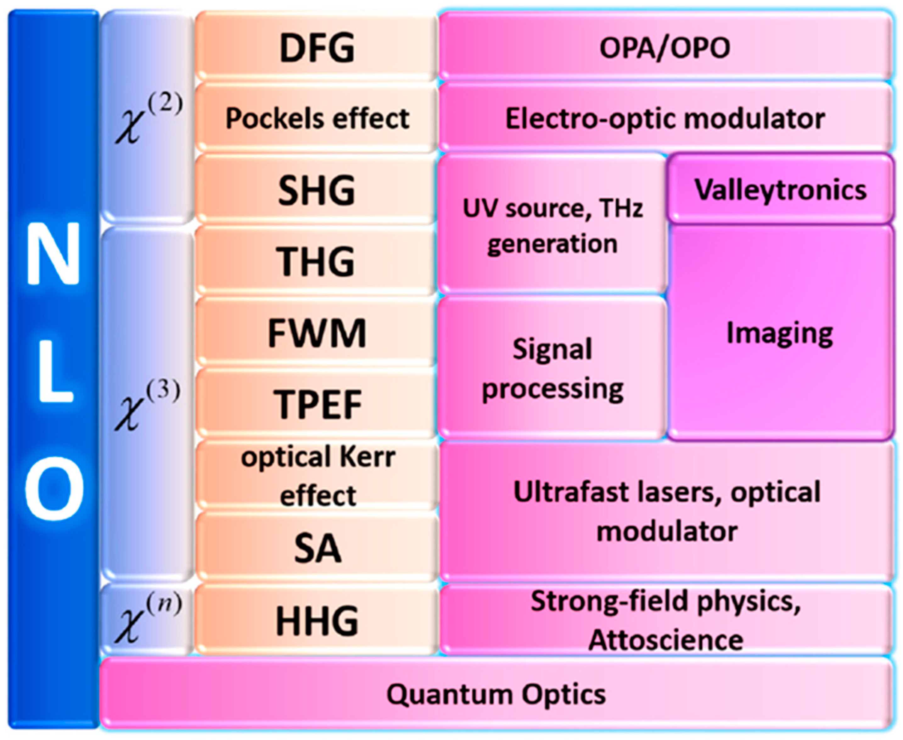
1. Introduction to Nonlinear Optics in 2D Materials

As a particular and interesting branch of modern optics, nonlinear optics mainly focus on the study of interaction between intense laser light and matter [1,2,3]. Shortly after the invention of the ruby laser in 1961, Franken et al. used a ruby laser with a wavelength of 694 nm to pass through a quartz crystal to generate ultraviolet light at 347 nm [4,5]. This is the earliest observed optical second harmonic generation (SHG) phenomenon, marking the birth of nonlinear optics. Nonlinear optics studies the phenomenon originating from the interaction between an intense laser with matter and has been widely used in laser generation, quantum optics, quantum computing, et al. [6,7,8,9,10]. Ordinary light sources with low intensity, such as sunlight and fluorescent lamps, cannot trigger the NLO responses, giving linear optical responses that obey superposition principles. Meanwhile, the intensity of a focused laser can reach 1015 to 1022 W/cm2, which means the electric field of the laser light source becomes comparable with that of the interatomic electric field (105 to 108 V/m) [11] and satisfies the requirement for a nonlinear response.
However, there are still many challenges in NLO applications, including high power loss [12], intricate nonlinear effects [13], and limited material response [14]. To solve these problems, researchers design high-performance platforms for integrated nonlinear optics to reduce the power loss [15], realize a large enhanced nonlinear response through resonant photonic nanostructures [16], and explore new materials with a high nonlinear coefficient [17]. Simultaneously, there are great challenges in integrating traditional nonlinear optical materials with other material platforms for on-chip applications [18,19]. Therefore, for future photonics and optoelectronics, it is very important to discover new materials with a large NLO response to meet the upcoming challenges through chip integration. These new materials are expected to provide innovative ways to enable new devices with new functions, high performance, and new device properties (e.g., reduced complexity, size, and cost, as well as a high nonlinear coefficient).
NLO materials include organic and inorganic materials. The most common organic NOL materials include 4-N,N-dimethylamino-4′-N′-methyl-stilbazolium tosylate (DAST) crystal [20], chromophores [21,22,23], et al. Organic NLO materials show excellent properties, such as a high electro-optical coefficient, easy-to-produce significant nonlinear polarization, fast response rate, high bandwidth, and good processability [24]. The disadvantage is that the carrier mobility of organic materials is generally low and the carrier recombination rate is low, which limits the modulation rate of organic terahertz modulation devices to a certain extent [24]. In this review, we mainly focus more on the nonlinear optical properties and control methods related to inorganic materials.
In recent years, 2D materials attracted more and more attention from researchers since the atomic-layer-thick graphene was successfully obtained with mechanical exfoliation [25]. Compared to their 3D counterparts, the atomically thin thickness of 2D materials exhibits unique electronic and optical properties due to reduced dielectric shielding and enhanced Coulomb interactions [26,27,28,29,30,31,32]. With the advantages of an ultra-broadband absorption and large nonlinear optical response of 2D materials, they can be widely used in numerous nonlinear applications. For example, optical communication [33], frequency conversion [34,35], imaging and characterization [36,37], electro-optic modulators [38,39], mode-locking [40,41,42], and Q-switching [43]. Investigation and modification of the NLO properties of 2D materials facilitate the evolution of optical and optoelectronic devices.
In this review, we survey recent progress of NLO properties including SHG, THG, and 2PPL in 2D materials, and discuss effective methods for the realization of dynamic control of NLO properties. We first briefly describe the physical mechanisms of the nonlinear optical process of SHG, THG, and 2PPL and the phase-matching conditions in materials. Then, we mainly focus on the nonlinear optics characterization applied in 2D materials, i.e., layer number, crystal orientation, grain boundary, and probing excitonic states. Furthermore, we discuss different methods such as carrier injection, strain, artificially stacking, as well as plasmonic enhancement control to realize the dynamic control of nonlinear optical signals in 2D materials. Finally, we summarize the advantages and disadvantages of different control methods, and present a perspective of potential research topics.

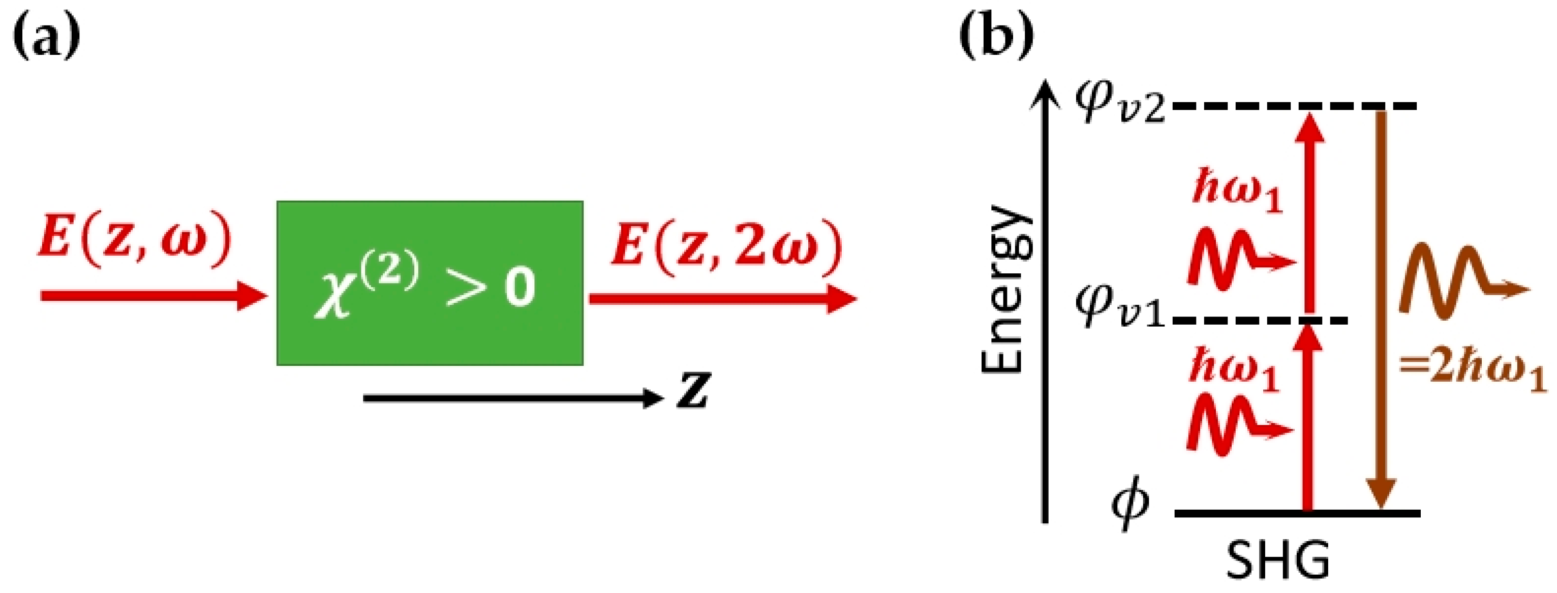
1.1. Second Harmonic Generation (SHG)

For the nonlinear process, the light-induced polarization P ~ t is a power series of electric field E ~ t , which can be described mathematically with the following equations [44,45]:
P ~ t = ϵ 0 [ χ 1 E ~ t + χ 2 E ~ t 2 + χ 3 E ~ t 3 + ] P ~ 1 t + P ~ 2 t + P ~ 3 t +
where ϵ 0 represents the vacuum permittivity and χ 1 is the linear susceptibility, which plays a role in the linear process such as absorption. χ 2 is the second-order NLO susceptibility, which determines processes such as the sum and difference frequency generation and electro-optic rectification. χ 3 , the third-order NLO susceptibility, is related to the third-order nonlinear effect, such as the third harmonic generation (THG) and two-photon photoluminescence (2PPL), four-wave mixing, Kerr lens effect, self-focusing, and white light generation with self-phase modulation [46]. The relationship between different orders of nonlinear susceptibilities and their applications is shown in Figure 1. P ~ 1 t   and P ~ n t (n > 1) are the induced linear polarization and nonlinear polarization, respectively.
Sum frequency generation occurs when two input photons with the frequency of ω 1 and ω 2 are combined, generating one photon with frequency ω 3 due to the second-order nonlinear polarization. This is a parametric process that obeys the energy conservation, i.e., ω 1 + ω 2 = ω 3 . SHG is a special case of sum frequency generation, where only one input laser exists. Hence ω 1 = ω 2 and ω 3 = 2 ω 1 . The transition energy level diagram of SHG is represented in Figure 2; here, the | ϕ represents the ground state, and the | φ v 1 and the | φ v 2 denotes two virtual states.

1.1.1. Time and Spatial Inversion Symmetry

The second harmonic signal will vanish for the medium with inversion symmetry (as demonstrated below). When E changes to the reverse direction, i.e., E ~ t = E ~ t , the polarization P ~ t will flip the sign and become P ~ t accordingly:
P ~ t = χ 2 ( E ~ t ) 2
According to Neumann’s principle, which indicates that the susceptibility tensor must be invariant by all the symmetry operators of the medium, the χ 2 should be unchanged. Thus, combine P ~ t =   χ 2 ( E ~ t ) 2 and P ~ t =   χ 2 ( E ~ t ) 2 , and we obtain χ 2 = 0. An expansion is that all the even-order susceptibility must be 0 for the medium with inversion symmetry.

1.1.2. Phase-Matching Condition

The phase-matching condition should be achieved in order to achieve high conversion efficiency for nonlinear bulk crystal, which means Δ k should be equal to zero ( Δ k = k 1 + k 2 k 3 ) [48,49]. The momentum conservation determines this equation. The momentum of foundational frequency and the frequency doubling light can be described with the momentum conservation:
P 2 ω = n 2 ω 2 ω c 0   and   P ω = n ω ω c 0
where the is the reduced Planck constant; c 0 is the speed of light in the vacuum; ω is the angular frequency; and n 2 ω and n ω are the refractive indicies of the doubling frequency and the incident frequency, respectively. Due to the dispersion, generally, the refractive index of 2 ω is larger than ω , making the condition of P 2 ω = P ω hard to fulfil. The phase matching can be achieved with birefringence.

1.2. Third-Order NLO Processes

This section briefly introduces two typical third NLO processes relevant to the research work on THG and 2PPL presented in this thesis. THG is similar to SHG, where three photons with the same energy ω 1 are absorbed simultaneously, followed by generating a new photon with the energy of 3 ω 1 . Figure 3a depicts the principle of THG. Unlike the χ 2 that will vanish in crystal with inversion symmetry, χ 3 always exists, independent of the crystal symmetry. However, χ 3 is generally orders of magnitude weaker than χ 2 for frequency conversion crystal [50]. An explanation from the perspective of quantum mechanics is that the possibility of three photons being present simultaneously is much less than two [51,52].
2PPL is induced with the two-photon absorption (TPA), an NLO absorption process involving simultaneous absorption of two photons and the transition from the ground state to the excited state [53]. After that, one photon with fixed energy is emitted, and the semiconductor decays back to the ground state, as shown in Figure 3b. Due to almost the same photoluminescent process, the emission spectra of 2PPL should generally possess a similar shape, peak position, and lifetime compared to the PL spectra [54,55,56,57,58].
It is easy to confuse the 2PPL with SHG, as 2PPL and SHG processes have some similarities, including the quadratic dependence of emission intensity on the excitation intensity. However, they are different: the emission of SHG is from a virtue state, whereas that of 2PPL originates from the real states. In other words, SHG is parametric while 2PPL is nonparametric, which involves absorption and energy relaxation.
Finally, it is worth noting that one-photon and two-photon processes obey different selection rules. As the optical section rule relies on the final state symmetry, transitions of one-photon excitation are only allowed for final states with even parity (such as the s state), while the two-photon excitations can reach final states with odd parity (such as the p state). Thus, unlike linear optics, information about dark excitons can be probed from the wavelength-dependent 2PPL and SHG.

2. Nonlinear Optics Characterization of 2D Materials

Two-dimensional materials with atomic layer thickness have large nonlinear optical coefficients and have attracted more and more attention. At the same time, since the nonlinear optical signals of 2D materials including SHG, THG, and 2PPL signals are very sensitive to the thickness, crystal phase, crystal axis orientation, grain boundary, and excitonic state of the material, nonlinear optics (NLO) spectroscopy can serve as a rapid, nondestructive, and accurate characterization method for 2D materials.

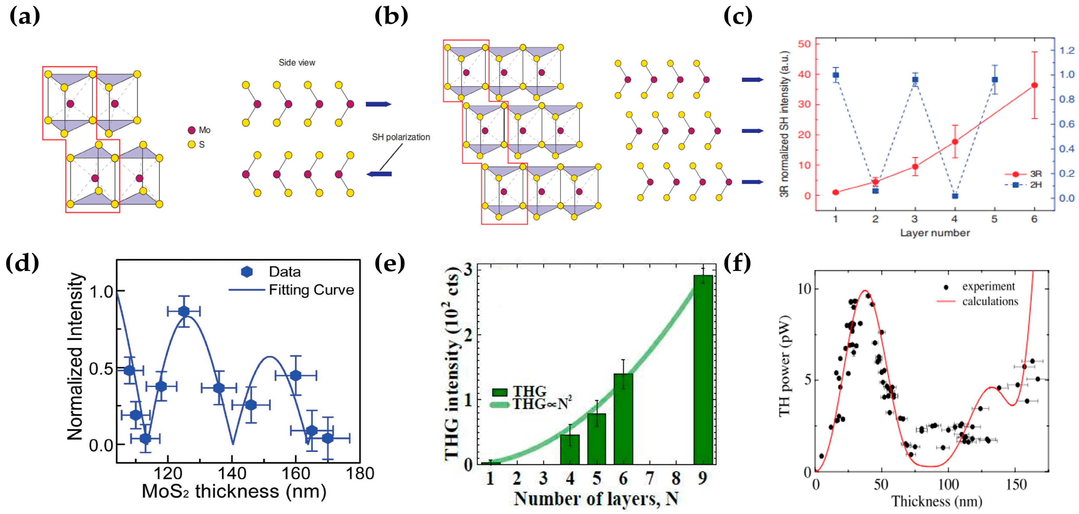
2.1. Determining the Layer Number

Among 2D materials, transition metal chalcogenides (TMDCs) such as MoS2, WS2, WSe2, hBN, etc., have become the most popular research objects because of their excellent charge-carrier mobility, high nonlinear coefficients, and high switching ratio [59,60,61]. TMDC materials are relatively common and stable in nature mainly in 1T, 2H, and 3R crystal phases [62,63,64]. As we discussed above, SHG will vanish for the medium with inversion symmetry [65]. Xiang Zhang et al. reported an SHG generated from the 2H and 3R crystal phase of MoS2 and discussed the relationship between SHG intensity and thickness in thin-layer (1~6L) MoS2 [66]. As shown in Figure 4a, the odd layers of the 2H phase retain a net nonlinear dipole with noncentral inversion symmetry, whereas centrosymmetric even layers exhibit a zero second-order nonlinear coefficient. Therefore, the SHG intensity oscillates with the layer number in the 2H thin layer as exhibited in Figure 4c. Contrary to 2H-phase crystal, 3R MoS2 maintains broken inversion symmetry from the monolayer to bulk, and the layers retain the same orientation but shift along the in-plane direction, and leads to parallel in-plane nonlinear dipoles as shown in Figure 4b. When the thickness of the 3R MoS2 is less than half of the coherence length (L) between the fundamental incident laser and SH signal [67], the SHG intensity of 3R MoS2 (for 1–5 layers) is proportional to the square of its thickness as can be seen from Figure 4c. If the thickness of 3R MoS2 is larger than the coherent length, the optical path difference (OPD) between the upper and lower surface of thicker 3R MoS2 needs to be considered. A model including bulk nonlinear coefficient contribution and interface interaction (MoS2–air/MoS2–substrate interfaces) is proposed by Xinfeng liu et al. [68]. The distribution of SHG intensity oscillations with thickness can be well explained using this model (Figure 4d).
Unlike SHG, THG can exist in structures with central inversion symmetry. José C. V. Gomes et al. studied the dependency between THG and the number of layers in WSe2 [69]. The results indicate that for thin-layered WSe2 (1~9L), the THG intensity is proportional to the square of the layer number (N2) as shown in Figure 4e. This quadratic scaling with thickness serves as direct evidence that each layer contributed independently to the overall THG, since the third-harmonic susceptibility of the N layer is proportional to that of the single layer: χ N ( 3 ) = N × χ s ( 3 ) .
Similar to SHG, the influence of interference effects needs to be considered for dependence of the THG intensity on the thickness in thick-layered 2D materials. Vladimir O. Bessonov et al. reported THG intensity versus thickness on thicker-layered hexagonal boron nitride (hBN) and explained that the THG signal generated with the surface layer interferes with the generation of deeper layers, leading to a decrease in THG intensity [70]. In addition, the second interface (hBN/substrate) will affect the location of maxima and minima in the thickness dependence of THG (Figure 4f). Since SHG relies on the broken inversion symmetry, it can be used to judge parity layers in 2H-phase 2D materials. The distribution relationship between the SHG/THG signal intensity of 3R-phase/all-phase 2D materials and the thickness can be inferred according to the model considering the interface interference effect.

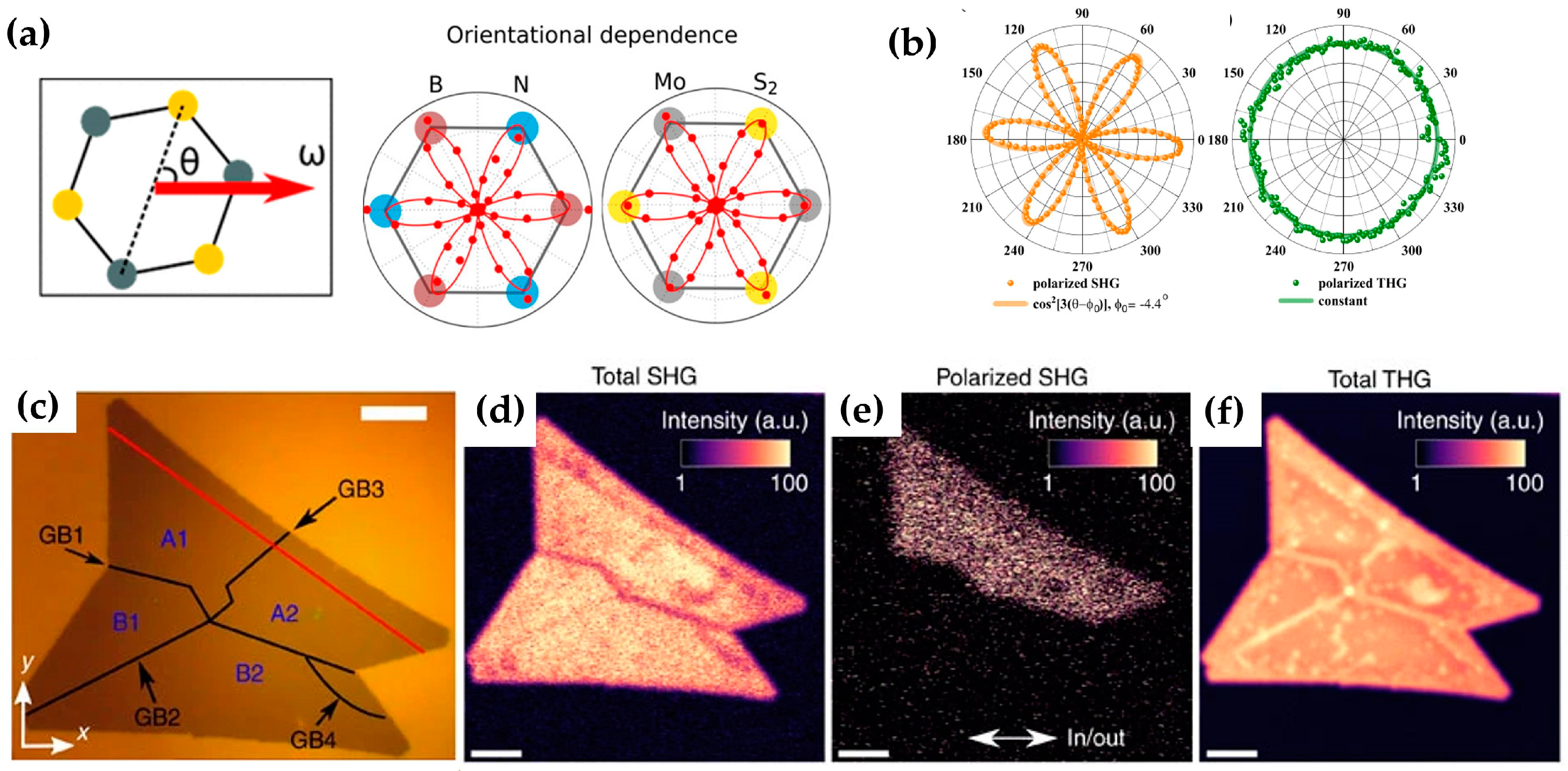
2.2. Crystal Orientation Identification and Mapping the Grain Boundary

Since crystal orientation and grain boundaries play a major role in the physical properties of two-dimensional layered materials, it is important to find efficient characterization methods to visualize them. Compared with traditional angle-resolved Raman spectroscopy [71,72], X-ray diffraction (XRD) [73,74], high-resolution transmission electron microscopy (HR-TEM) [75,76], and other characterization methods, the advantages of a high speed and nondestructive characterization have made nonlinear optical spectroscopy a powerful method for determining the orientation of the crystal axis and mapping the grain boundary.
Because the effective second-order nonlinear coefficients d e f f = 1 / 2 χ ( 2 ) are highly correlated with structural symmetry, angle-resolved SHG can be used as a fast and nondestructive characterization method for the crystallographic orientation of 2D materials. The polarization direction of the SHG depends on the direction of the incident electric field and d e f f of the materials, which can be expressed with the following function [37]:
E 2 ω e ^ 2 ω = C e ^ 2 ω χ 2 : e ^ ω e ^ ω
I S H G = e ^ 2 ω d e f f e ^ ω 2 2
where e ^ ω and e ^ 2 ω represent the direction of the incident and outgoing electric field, C is the scaling factor that includes the local electric field factor. In the 2H-phase 2D materials (like hBN, MoS2, etc.), the odd-numbered layer structure belongs to the D3h point group. Through the simplification of crystal symmetry, d e f f satisfied the matrix as follows:
d e f f = 0 d 21 0 0 d 22 0 0 0 0 0 0 0 0 0 0 d 16 0 0
Among them (d21 = d16 = −d22), if the incident light is perpendicular to the sample and the incident electric field is projected onto the armchair direction of the sample as shown in Figure 5a, the parallel and perpendicular SHG of 2H-phase TMDCs can be written as
I = I 0 c o s 2 3 θ
I = I 0 s i n 2 3 θ
Here, θ represents the azimuth angle of the material, and I 0 is the maximum intensity of the SHG. Since θ = 0 ° corresponds to a direction where the polarization of the pump beam is along the armchair direction, the SHG intensity reaches its largest state. Tony F. Heinz and José C. V. Gomes et al. found that the SHG intensity polar plot of odd-layered hBN, MoS2, and WSe2 exhibits a six-lobed shape, which corresponds to the D3h symmetry as shown in the right side of Figure 5a and the left side of Figure 5b, respectively [69,77]. In contrast, José C. V. Gomes et al. carried out the polarization-dependent THG measurement on monolayer WSe2 and reported that the intrinsic THG response is independent of the incident polarization (Figure 5b) [69]. Kaihui Liu et al. also performed a similar experiment and monitored the pattern evolution in monolayer WS2 [78]; the results confirmed that the generated THG satisfied the relationship with the polarized incident laser, I = I 0 , I = 0 , which means that THG is polarization-independent. Polarization-resolved nonlinear spectroscopy can identify the crystal axis orientation, while a THG image can realize the visualization of grain boundaries. Lasse Karvonen et al. carried out multiphoton (SHG and THG) characterization studies by scanning a laser beam over the MoS2 flakes (Figure 5c) with two galvo mirrors; SHG and THG images obtained without an analyser in front of the detector are shown in Figure 5c,f [79]. In the total-SHG image, only GB1 appears as dark due to the destructive interference of the SHG fields from the neighbouring grains [80]. Figure 5e presents results for polarized SHG imaging (parallel-polarized excitation and detection); only the area above GB1 is visible, suggesting a large difference between the upper (A1 and A2) and lower (B1 and B2) parts, which indicates that the polarized SHG image can resolve the crystal orientations. The contrast difference between neighbouring grains is due to the anisotropic polarization pattern of SHG [60], and the occurrence of destructive interference depends on whether the edges of the neighbouring grains are of the same type and the incident light polarization is perpendicular to the bisecting direction of the grain edges [81]. Contrasting the SHG image, all the GBs (GB1-GB4) can be clearly seen from the THG image (Figure 5f). Since THG does not depend on the parity of the layer number and exhibits no polarization dependence on the crystallographic axis angle, a THG image can serve as a rapid and sensitive visualization method of grain boundaries.
Figure 5. (a) Left: schematic diagram of the atomic structure of TMDC material, where θ represents the azimuth angle of the material. The angle θ = 0 ° corresponds to a direction where the polarization of the pump beam is along the armchair direction. Right: schematic view of SH intensity polar plot of monolayer hBN and MoS2; (b) polarization-dependent SHG and THG of WSe2; (c) optical image of MoS2 with marked grains (A1, A2, B1, and B2) and grain boundaries (GB1, GB2, GB3, and GB4); (d) experimental SHG mapping image of MoS2 without analyser, scale bars: 10 μm; (e) experimental SHG image with parallel polarized excitation and detection; (f) experimental THG mapping of MoS2 without analyser; panel (a) adapted with permission from Ref. [77], Copyright 2013, American Chemical Society; panel (b) adapted with permission from Ref. [69], Copyright 2018, American Chemical Society; panel (cf) adapted with permission from Ref. [79], Copyright 2017, Nature communications.
Molecules 28 06737 g005

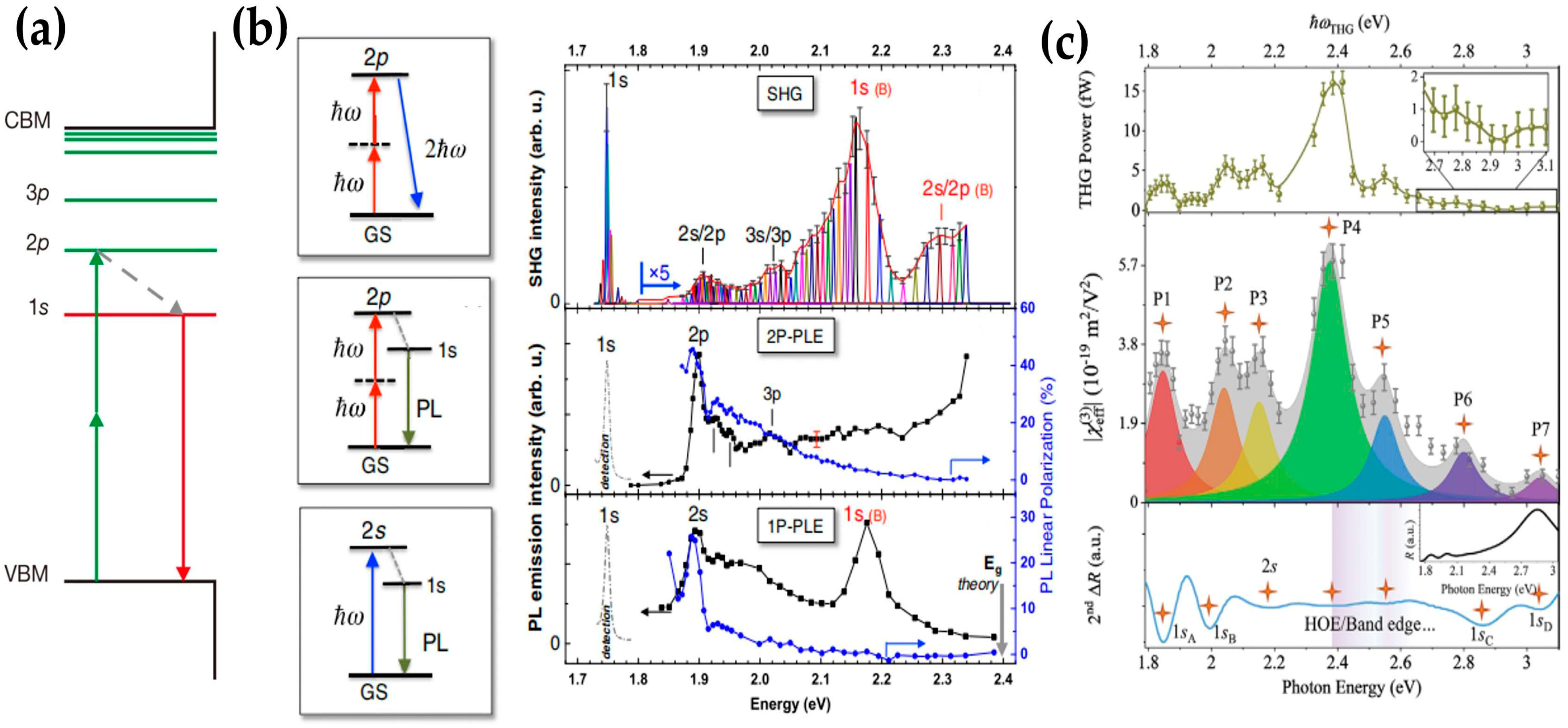
2.3. Probing Excitonic State

Monolayer TMDs with atomic thickness usually exhibit a strong Coulomb interaction as a result of reduced dielectric screening effects. This leads to the formation of a series of discrete excitonic states near the band edge called “Rydberg” excitons [82,83,84]. As can be seen from Figure 6a, the “Rydberg” excitonic states below the quasiparticle bandgap generally exhibit electronic energy levels analogous to the hydrogen series labelled as 1s, 2p, 3p, and so on [85]. If the incident electromagnetic wave is in resonance with the energy of the exciton states, light–matter interaction will be significantly enhanced [86,87]. Whether it is the giant PL emission enhancement [88,89] or the nearly 100% light absorption near the exciton state [90], it proves the existence of the exciton resonance effect. Similarly, the exciton resonance effect in TMDs is also applicable to its nonlinear optical properties. For example, signals of SHG, 2PPL, and THG can be greatly enhanced by up to three orders of magnitude if the excitation energy is resonant with the corresponding excitonic state. Based on the symmetry selection rules of electronic transition, a one-photon excitation process can only reach states with even parity (dipole-allowed bright states) while two-photon transitions can reach odd-parity states with nonzero orbital angular momentum. This means that bright states like “ns” can be detected with optical reflectance spectroscopy [82,83] or photoluminescence (PL) excitation (PLE) spectroscopy [91]. The dark states like “np” and “nd” can be probed with two-photon photoluminescence excitation (2PPLE) spectroscopy [85]. Since the generation of an SHG signal is the combination of electric–dipole (ED) and magnetic–dipole (MD) optical transitions, SHG excitation spectroscopy (SHGE) can probe both even (“s”) and odd (“p”) parity states [92]. The generation of THG does not depend on the broken inversion symmetry, and its resonance excitonic energy is high. Therefore, it can not only detect bright “ns” states but also high-energy excitonic states like C and D excitons.
Based on the above principle, G. Wang et al. carried out an SHGE, PLE, as well as 2PPLE experiment on monolayer WSe2 at 4K as shown in Figure 6b and the excitation power was kept constant in the experiments [92]. According to the transition selection rule discussed above, the SHGE spectrum detects “1s”, “2s/2p”, and “3s/3p” excitonic states of the A exciton as well as “1s” and “2s/2p” excitonic states of the B exciton. However, the energy difference between the “s” and “p” states is too small to distinguish from the SHGE spectrum. Since 2PPLE and PLE can only detect dark “p” states and bright “s” states, respectively, combining them with SHGE can achieve a detailed identification of Rydberg exciton states. Ziliang Ye et al. also similarly probed the excitonic effects in monolayer WS2 and demonstrated that there is no significant shift in the excitation energy of either the “s” or the “p” states with different capping layers by measuring 2PPLE of monolayer WS2 with different dielectric capping layers, including water, immersion oil, and aluminium oxide [85]. Yadong Wang et al. demonstrated broadband THGE (≈1.79 to 3.10 eV) in monolayer MoS2 to explore prominent fingerprints of excitonic states including “s” series excitons and free-band electronic states [93]. As exhibited in Figure 6c, remarkable THG enhancement at certain photon energies has been observed and the effective third-order nonlinear susceptibility at different THG energies was calculated. By fitting the peak labelled as P1-P7 in Lorentzian functions and comparing that with the second-order differential of the reflectance spectrum, the authors successfully identified “1s” and “2s” of the A exciton as well as the 1s state of B, C, and D excitonic states with a higher energy level.
Therefore, broadband and high-contrast nonlinear optical spectrums can serve as new characterization methods to uncover several relevant electronic states such as bright s series, dark excitons, as well as band-edge excitonic states. This nondestructive and fast method of determining the excitonic state facilitates our further study of the physical properties related to the exciton in 2D materials.

3. Tuning Methods

Nonlinear light-matter interaction in atomically thin TMD is important for both fundamental research and future optoelectronic devices. In recent years, researchers have tried different methods such as carrier injection, strain, artificially stacking, as well as plasmonic enhancement control to realize the dynamic control of nonlinear optical signals.

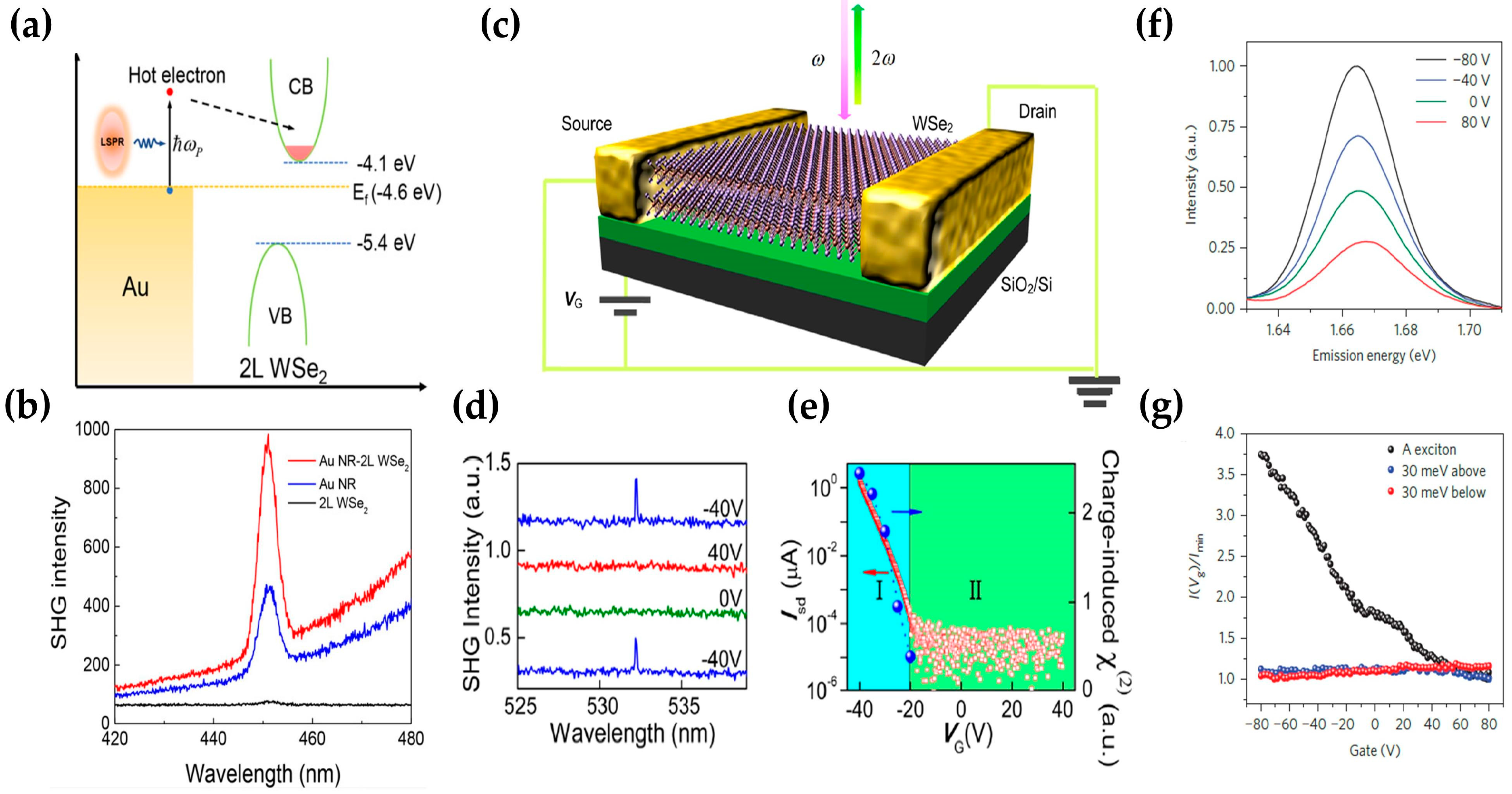
3.1. Carrier Injection Tuning
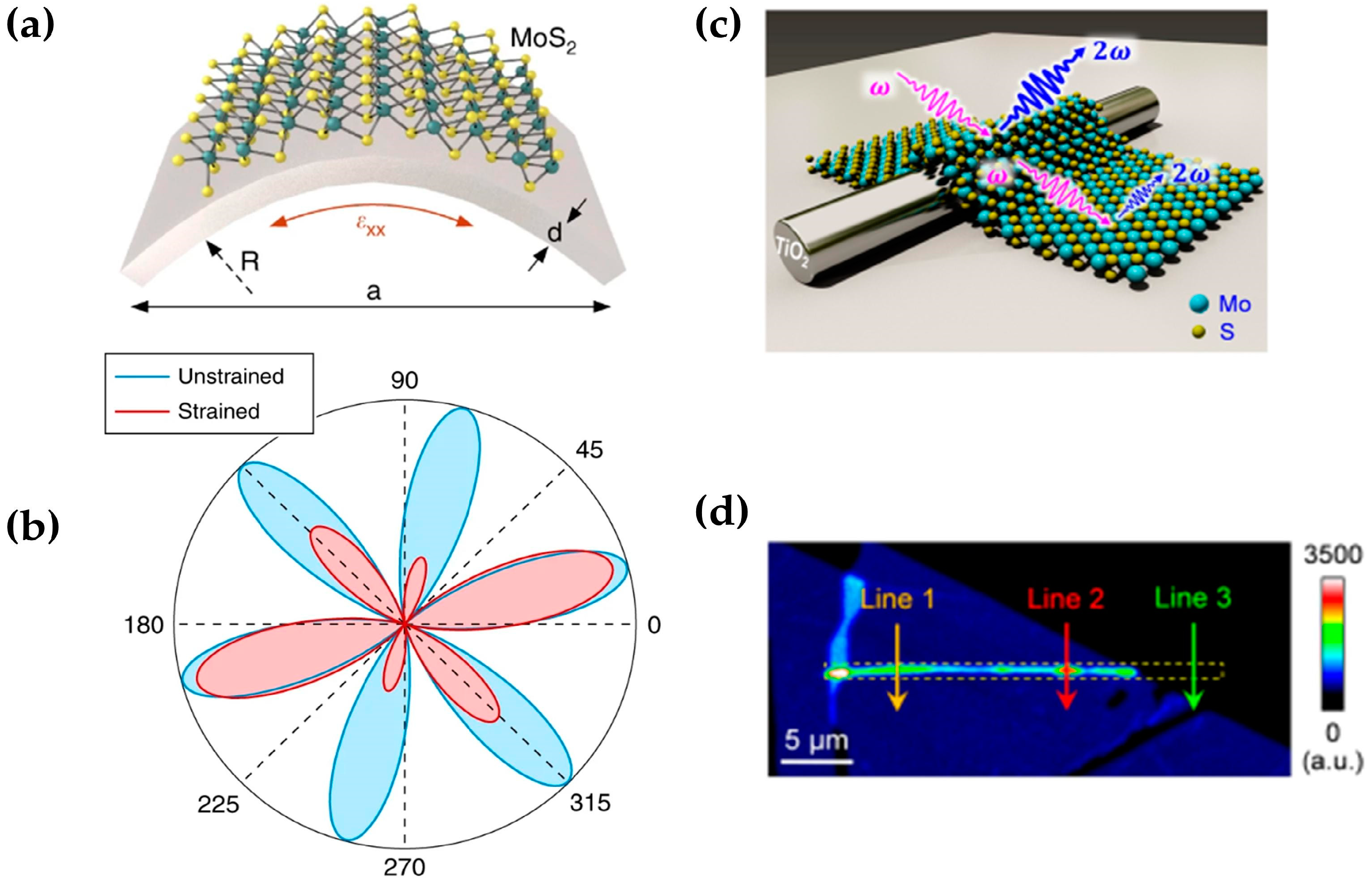
Xiong’s group demonstrated the emergence of an SHG signal in 2L WSe2 with plasmonic hot-electron injection as shown in Figure 7a [94]. The SHG is absent in 2L WSe2 due to the centrosymmetry; however, when the gold nanorod is coupled with 2L WSe2, the SHG signal of the bilayers changes from nothing to a presence as shown in Figure 7b. Under the excitation of an 850 nm pump laser, only the plasmonic metal can be excited, and the rise time around 120 fs and the decay lifetime around 1 ps are consistent with that of plasmonic hot-electron generation and transfer time. The mechanism involved was considered to be the broken inversion symmetry in 2L WSe2 with hot-electron injection and thus inducing an SHG. Similarly, Xiong’s group also demonstrated manipulation of the bond charges in a 2L WSe2 by applying a perpendicular electric field. They reported the charge-induced SHG (CHISHG) from the 2H-2L-WSe2-based back-gate field transistors, shown in Figure 7c–e [95]. Under the gate voltage of −40 V, the SHG intensity from bilayers was found to be 1000 times weaker than that from the monolayer. There is a charge (hole) accumulation in the sample and efficient SHG can be observed, as shown with the back-gate sweep of source-drain current Isd in Figure 7e. The authors explained the origination of SHG with a bond charge model: charge accumulation in the W metal planes leads to a nonuniform electric distribution, which breaks the symmetry of bilayers. In another work, Xiaodong Xu et al. reported the electrical control of SHG intensity regarding a monolayer WSe2 field-effect transistor [39]. They chose the electrostatic doping method induced with strong exciton charging effects in monolayer TMD materials. If the two-photon excitation energy is resonant with the A exciton as shown in Figure 7f, the resonant SHG can be tuned with electrostatic doping and exhibits a nearly four-fold intensity reduction and gate voltage (Vg) is swept from −80 to 80 V. If the two-photon excitation energy is 30 meV above or below the exciton resonance, Vg has no effect on the SHG (Figure 7g), supporting the idea that the SHG tuning originates from the modulation of oscillator strength at the exciton resonance.

3.2. Strain Tuning

Mechanical strain can deform the crystal lattice, thus enabling the modulation of SHG. For example, Mennel et al. found that strain can alter the polarization dependence of SHG for monolayer MoS2 [96]. Figure 8a,b show that under the 1% strain, the polarization pattern of SHG deforms along the uniaxial strain. Electric gating and charge injection can also be utilized to break the symmetry, and this fascinating property is only possible in TMDCs. In another work, Li et al. reported a heterostructure combining mechanically exfoliated MoS2 and TiO2 nanowires and realized the modulation of the second harmonic polarization of MoS2 through the spontaneous strain of different orientations, as shown in Figure 8c [97]. The MoS2/TiO2 heterojunction region is ten times stronger than the SHG of monolayer MoS2, while the region of pure TiO2 does not produce any signal. It proves that the enhancement of the second harmonic signal in this heterojunction region does not originate from titanium dioxide direct contribution, as shown in Figure 8d. Therefore, in layered 2D materials, since the second harmonic is very sensitive to strain, strain modulation of the second harmonic in 2D materials is very promising.

3.3. Artificially Stacking

SHG is highly sensitive to lattice symmetry and crystallographic axis orientation of the material. Hence, it can be modulated with artificial symmetry control, such as manipulating the adjacent layer alignment and applying external stimulation. Lin et al. stacked multiple triangular WS2 sheets in a concentric manner to form a pyramid, shown in Figure 9a [98]. With the number of layers superimposed, the SHG intensity will show a trend of decreasing oscillation similar to that of 2H. With more than 70 layers, the SHG intensity will significantly occur. The main reason for the enhancement is due to the edge SHG enhancement of the multilayer structure, which will eventually be 45 times stronger than that of a single layer, as shown in Figure 9b. Furthermore, Fan et al. reported a detailed SHG study of spiral WS2 multilayer nanosheets with a twisted angle of 5 degrees, as shown in Figure 9c [99]. In contrast to the diminishing oscillation of normal 2H-phase WS2, the SHG intensity of spiral WS2 increases with the layer number (see Figure 9d). This spiral WS2 with enhanced SHG signals in multilayers extends the NLO application of TMDCs. Hsu et al. in 2014 first started the investigation of SHG in TMDC heterostructures. They fabricated chemical vapor deposition (CVD)-grown homo-stacked MoS2/MoS2 and studied the SHG generation with different stacking angles, as shown in Figure 9e [100]. Their experiment demonstrated that SHG from the artificial bilayer is a coherent superposition of that from individual layers, with a phase difference determined with the stacking angle. For a bilayer with a 2H stacking order (θ = 60°), the SHG totally vanishes, and for a 3R stacking order AA (θ = 0°), the SHG is nearly three times stronger than that from the monolayer, shown in Figure 9f. In addition to stacking the same TMDC material, there is also the stacking of different materials to form a heterojunction structure to enhance the SHG and THG. Zhang et al. fabricated a typical monolayer WS2 (WSe2) and MoS2 (MoSe2) heterostructure, keeping its triangular domain shape, as shown in Figure 9g [101]. Figure 9h,i show the parallel-polarized SHG images of the lateral heterostructures of WSe2-MoSe2 and WS2-MoS2, respectively. The maximum SHG image of the lateral heterostructure of WS2-MoS2 was obtained at the position of θ = 0°.

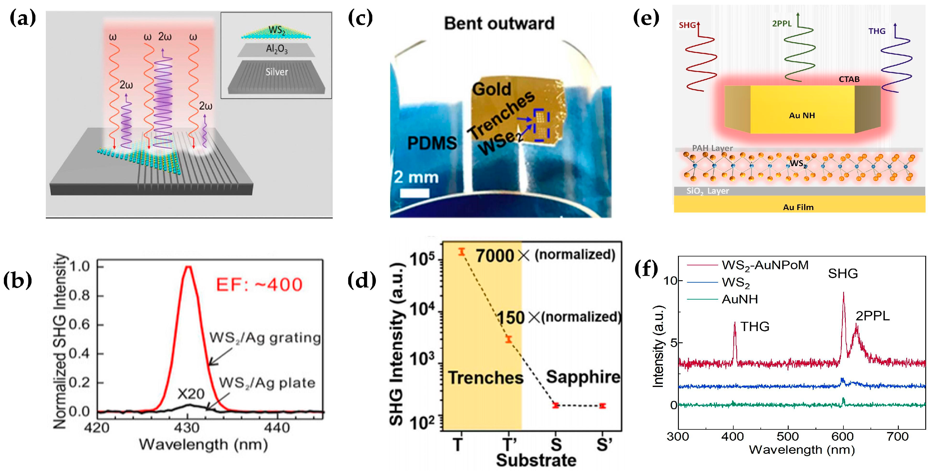
3.4. Plasmonic Enhancement

There are two types of plasmons: localized surface plasmons and surface plasmons. Surface plasmons refer to the collective oscillation of free electrons on the metal surface when light is incident on the interface between the metal and the dielectric. When the frequency of the incident light is the same as the oscillation frequency of the electrons, the electromagnetic field will be confined on the metal surface and generate. The enhancement of the local electric field generated with plasmons can effectively improve the conversion efficiency of the second harmonic. Local surface plasmons can effectively confine light to the sub-wavelength region, thereby significantly enhancing the local electromagnetic field. Shi et al. reported a 400-fold SHG enhancement by coupling the monolayer WS2 to the 2D Ag nanogrooves. as shown in Figure 10a [102]. The resonant electric field inside the nanogroove was designed at 430 nm, overlapping with the C exciton resonance in WS2. In addition, the presence of grooves provides much stronger enhancement than that with the Ag plant, as shown in Figure 10b. Wang et al. combined the flexible substrate PDMS with a single layer of WS2 to design a surface plasmon structure [103], which achieved a second harmonic enhancement of more than three orders of magnitude, as shown in Figure 10c. A 7000-fold SHG enhancement at the channel was finally obtained by controlling the size of the strip structure, as shown in Figure 10d. Previously, SHG or THG was enhanced separately, and SHG and THG were not enhanced at the same time. Shi et al. designed a hybrid nanostructure of monolayer WS2 integrated with a plasmonic cavity as shown in Figure 10e [104]. Optimum 1000-, 3000-, and 3800-fold enhancement was achieved for two-photon photoluminescence, second harmonic generation, and third harmonic generation, respectively, in the optimized cavity structure, which is composed of the Au/SiO2 (50 nm/10 nm) substrate, monolayer WS2, PAH, and CTAB-coated single AuNH, as shown in Figure 10f. Meanwhile, results show that plasmon enhanced NLO spectroscopy could serve as a general method for probing high-order Rydberg excitonic states of 2D materials. With the maturity of the surface plasmon technology and the in-depth understanding of the localized surface plasmon resonance, it is possible to design a more refined structure that can better confine the incident electric field in the future to increase the SHG and THG.

4. Summary and Outlook

In this review, we summarize the research progress on typical nonlinear optical (NLO) processes in 2D materials, including SHG, THG, and 2PPL. It is worth noting that for 2D materials, not only the inorganic TMD materials mentioned in the review show interesting nonlinear optical properties but also organic 2D materials such as covalent organic frameworks (COFs), metal–organic frameworks (MOFs), and chromophore-conjugated nanomaterials exhibit attractive nonlinear optical properties, especially the giant two-photon absorption (2PA) [105,106,107]. For example, fullerene derived with chromophore-conjugated nanomaterials corresponds to 2D characters due to the interactive fullerenyl hydrophobic intermolecular interaction forces and exhibits large cross-sections of 2PA [108,109]. Compared to 2D inorganic materials, molecular chromophores are advantageous in larger cross-sections and tuning the 2PA properties with different functional groups; however, it is challenging to precisely control the spatial arrangement of the chromophores and the chromophore molecules usually exhibit poor orientation stability [24]. For inorganic 2D TMD materials, they have good stability and exhibit a high SHG and THG nonlinear coefficient. However, their 2PPL signals are still relatively limited due to their weak quantum efficiency and small cross-section. Therefore, appropriate enhancement and regulation methods are still urgent issues that researchers need to solve.
In addition, we demonstrate that the nonlinear optical spectroscopy can serve as a characterization method for 2D materials such as determining the layer number, crystal orientation identification, and mapping the grain boundary and probing excitonic state. By means of carrier injection tuning, strain tuning, artificial stacking, and surface plasmon enhancement, nonlinear optical signals in 2D materials can be effectively modulated. Table 1 shows the above kinds of regulation methods and modulation effects.
The NLO feature has the characteristics of high-speed measurement, nondestructive measurement, large-area measurement, and multi-mode. Combining different tuning methods can have a large number of applications in optoelectronic devices like all-optical devices, photonic information communication, and even nonlinear optical valleytronics. For example, combining the plasmonic modulation and nonlinear optical signals can be applied in the application of nonlinear valleytronics in TMDC materials [110,111]. The use of strain tuning as well as excitonic resonant excitation can broaden the modulation depth and range and further improve the performance of the NLO response of TMDC [112].
Finally, for the future development direction, we can explore the nonlinear optical properties of new 2D materials and their heterostructures such as 2D magnetic materials and related control methods, and create highly stable and high-quality nonlinear optical integrated devices to broaden their application fields in semiconductor electronics, spin valley electronics, and other fields.

Author Contributions

J.S. and S.F. contributed equally. Conceptualization, J.S., S.F., P.H., Y.F. and X.Z.; investigation, J.S. and S.F.; writing—original draft preparation, J.S. and S.F.; writing—review and editing, J.S., S.F., P.H., Y.F. and X.Z.; supervision, J.S., P.H., Y.F. and X.Z.; project administration, J.S.; funding acquisition, J.S. All authors have read and agreed to the published version of the manuscript.

Funding

This research was funded by the China Postdoctoral Science Foundation, grant number: 2023M730155.

Institutional Review Board Statement

Not applicable.

Informed Consent Statement

Not applicable.

Data Availability Statement

Not applicable.

Acknowledgments

We thank Jing Li for him inviting us to write the paper.

Conflicts of Interest

The authors declare no conflict of interest.

Sample Availability

Not applicable.

References

  1. Lahiri, A. Chapter 9—Nonlinear Optics. In Basic Optics; Elsevier: Amsterdam, The Netherlands, 2016; pp. 901–968. [Google Scholar] [CrossRef]
  2. Suresh, S.; Ramanand, A.; Jayaraman, D.; Mani, P. Review on Theoretical Aspect of Nonlinear Optics. Rev. Adv. Mater. Sci. 2012, 30, 175–183. [Google Scholar]
  3. Stolen, R.H. The Early Years of Fiber Nonlinear Optics. J. Light. Technol. 2008, 26, 1021–1031. [Google Scholar] [CrossRef]
  4. Barh, A.; Rodrigo, P.J.; Meng, L.; Pedersen, C.; Tidemand-Lichtenberg, P. Parametric Upconversion Imaging and Its Applications. Adv. Opt. Photon. 2019, 11, 952–1019. [Google Scholar] [CrossRef]
  5. Franken, P.A.; Hill, A.E.; Peters, C.W.; Weinreich, G. Generation of Optical Harmonics. Phys. Rev. Lett. 1961, 7, 118–119. [Google Scholar] [CrossRef]
  6. Garmire, E. Nonlinear Optics in Daily Life. Opt. Express 2013, 21, 30532–30544. [Google Scholar] [CrossRef] [PubMed]
  7. Chang, D.E.; Vuletić, V.; Lukin, M.D. Quantum Nonlinear Optics—Photon by Photon. Nat. Photonics 2014, 8, 685–694. [Google Scholar] [CrossRef]
  8. Agrawal, G.P. Nonlinear Fiber Optics: Its History and Recent Progress [Invited]. J. Opt. Soc. Am. B 2011, 28, A1–A10. [Google Scholar] [CrossRef]
  9. Wright, L.G.; Renninger, W.H.; Christodoulides, D.N.; Wise, F.W. Nonlinear Multimode Photonics: Nonlinear Optics with Many Degrees of Freedom. Optica 2022, 9, 824–841. [Google Scholar] [CrossRef]
  10. Corn, R.M.; Higgins, D.A. Optical Second Harmonic Generation as a Probe of Surface Chemistry. Chem. Rev. 1994, 94, 107–125. [Google Scholar] [CrossRef]
  11. Mourou, G.A.; Tajima, T.; Bulanov, S.V. Optics in the Relativistic Regime. Rev. Mod. Phys. 2006, 78, 309–371. [Google Scholar] [CrossRef]
  12. Zuo, Y.; Yu, W.; Liu, C.; Cheng, X.; Qiao, R.; Liang, J.; Zhou, X.; Wang, J.; Wu, M.; Zhao, Y.; et al. Optical Fibres with embedded Two-Dimensional Materials for Ultrahigh Nonlinearity. Nat. Nanotechnol. 2020, 15, 987–991. [Google Scholar] [CrossRef] [PubMed]
  13. Wang, X.; Zhou, P.; Su, R.; Ma, P.; Tao, R.; Ma, Y.; Xu, X.; Liu, Z. Current Situation, Tendency and Challenge of Coherent Combining of High Power Fiber Lasers. Chin. J. Lasers 2017, 44, 0201001. [Google Scholar] [CrossRef]
  14. Zheng, Y.; Maev, R.; Solodov, I. Review/Sythèse Nonlinear Acoustic Applications for Material Characterization: A review. Can. J. Phys. 2011, 77, 927–967. [Google Scholar] [CrossRef]
  15. Moss, D.J.; Morandotti, R.; Gaeta, A.L.; Lipson, M. New CMOS-Compatible Platforms Based on Silicon Nitride and Hydex for Nonlinear Optics. Nat. Photonics 2013, 7, 597–607. [Google Scholar] [CrossRef]
  16. Zubyuk, V.V.; Shafirin, P.A.; Shcherbakov, M.R.; Shvets, G.; Fedyanin, A.A. Externally Driven Nonlinear Time-Variant Metasurfaces. ACS Photonics 2022, 9, 493–502. [Google Scholar] [CrossRef]
  17. Gan, X.-T.; Zhao, C.-Y.; Hu, S.-Q.; Wang, T.; Song, Y.; Li, J.; Zhao, Q.-H.; Jie, W.-Q.; Zhao, J.-L. Microwatts Continuous-Wave Pumped Second Harmonic Generation in Few- and Mono-layer GaSe. Light. Sci. Appl. 2018, 7, 17126. [Google Scholar] [CrossRef]
  18. Sirleto, L.; Righini, G.C. An Introduction to Nonlinear Integrated Photonics: Structures and Devices. Micromachines 2023, 14, 614. [Google Scholar] [CrossRef]
  19. Bogdanov, S.; Shalaginov, M.Y.; Boltasseva, A.; Shalaev, V.M. Material Platforms for Integrated Quantum Photonics. Opt. Mater. Express 2017, 7, 111–132. [Google Scholar] [CrossRef]
  20. Tian, T.; Fang, Y.; Wang, W.; Yang, M.; Tan, Y.; Xu, C.; Zhang, S.; Chen, Y.; Xu, M.; Cai, B.; et al. Durable Organic Nonlinear Optical Membranes for Thermotolerant Lightings and In Vivo Bioimaging. Nat. Commun. 2023, 14, 4429. [Google Scholar] [CrossRef]
  21. Liu, J.; Ouyang, C.; Huo, F.; He, W.; Cao, A. Progress in the Enhancement of Electro-Optic Coefficients and Orientation Stability for Organic Second-Order Nonlinear Optical Materials. Dyes Pigm. 2020, 181, 108509. [Google Scholar] [CrossRef]
  22. Verbitskiy, E.V.; Achelle, S.; Bureš, F.; le Poul, P.; Barsella, A.; Kvashnin, Y.A.; Rusinov, G.L.; Guen, F.R.-l.; Chupakhin, O.N.; Charushin, V.N. Synthesis, Photophysical and Nonlinear Optical Properties of [1,2,5]Oxadiazolo[3,4-b]Pyrazine-based Linear Push-Pull Systems. J. Photochem. Photobiol. A 2021, 404, 112900. [Google Scholar] [CrossRef]
  23. Fecková, M.; le Poul, P.; Bureš, F.; Robin-le Guen, F.; Achelle, S. Nonlinear Optical Properties of Pyrimidine Chromophores. Dyes Pigm. 2020, 182, 108659. [Google Scholar] [CrossRef]
  24. Fuyang, H.; Zhuo, C.; Shuhui, B. Advances in Organic Second-Order Nonlinear Optical Polymers. J. Funct. Polym. 2020, 33, 108. [Google Scholar] [CrossRef]
  25. Novoselov, K.S.; Geim, A.K.; Morozov, S.V.; Jiang, D.; Zhang, Y.; Dubonos, S.V.; Grigorieva, I.V.; Firsov, A.A. Electric Field Effect in Atomically Thin Carbon Films. Science 2004, 306, 666–669. [Google Scholar] [CrossRef] [PubMed]
  26. Cipriano, L.A.; Di Liberto, G.; Tosoni, S.; Pacchioni, G. Quantum Confinement in Group III–V Semiconductor 2D Nanostructures. Nanoscale 2020, 12, 17494–17501. [Google Scholar] [CrossRef]
  27. Tareen, A.K.; Khan, K.; Aslam, M.; Liu, X.; Zhang, H. Confinement in Two-Dimensional Materials: Major Advances and Challenges in the Emerging Renewable Energy Conversion and Other Applications. Prog. Solid State Chem. 2021, 61, 100294. [Google Scholar] [CrossRef]
  28. Gupta, A.; Sakthivel, T.; Seal, S. Recent Development in 2D materials Beyond Graphene. Prog. Mater. Sci. 2015, 73, 44–126. [Google Scholar] [CrossRef]
  29. Novoselov, K.S.; Mishchenko, A.; Carvalho, A.; Castro Neto, A.H. 2D Materials and Van Der Waals Heterostructures. Science 2016, 353, aac9439. [Google Scholar] [CrossRef]
  30. Kim, Y.-J.; Kim, Y.; Novoselov, K.; Hong, B.H. Engineering Electrical Properties of Graphene: Chemical Approaches. 2D Mater. 2015, 2, 042001. [Google Scholar] [CrossRef]
  31. Manzeli, S.; Ovchinnikov, D.; Pasquier, D.; Yazyev, O.V.; Kis, A. 2D Transition Metal Dichalcogenides. Nat. Rev. Mater. 2017, 2, 17033. [Google Scholar] [CrossRef]
  32. Glavin, N.R.; Rao, R.; Varshney, V.; Bianco, E.; Apte, A.; Roy, A.; Ringe, E.; Ajayan, P.M. Emerging Applications of Elemental 2D Materials. Adv. Mater. 2020, 32, 1904302. [Google Scholar] [CrossRef] [PubMed]
  33. You, J.; Luo, Y.; Yang, J.; Zhang, J.; Yin, K.; Wei, K.; Zheng, X.; Jiang, T. Hybrid/Integrated Silicon Photonics Based on 2D Materials in Optical Communication Nanosystems. Laser Photonics Rev. 2020, 14, 2000239. [Google Scholar] [CrossRef]
  34. Yoshikawa, N.; Tamaya, T.; Tanaka, K. High-Harmonic Generation in Graphene Enhanced by Elliptically Polarized Light Excitation. Science 2017, 356, 736–738. [Google Scholar] [CrossRef] [PubMed]
  35. Liu, H.; Li, Y.; You, Y.S.; Ghimire, S.; Heinz, T.F.; Reis, D.A. High-Harmonic Generation from An Atomically Thin Semiconductor. Nat. Phys. 2017, 13, 262–265. [Google Scholar] [CrossRef]
  36. Dmowski, W.; Iwashita, T.; Chuang, C.P.; Almer, J.; Egami, T. Elastic Heterogeneity in Metallic Glasses. Phys. Rev. Lett. 2010, 105, 205502. [Google Scholar] [CrossRef]
  37. Malard, L.M.; Alencar, T.V.; Barboza, A.P.M.; Mak, K.F.; de Paula, A.M. Observation of Intense Second Harmonic Generation from MoS2 Atomic Crystals. Phys. Rev. B 2013, 87, 201401. [Google Scholar] [CrossRef]
  38. Klein, J.; Wierzbowski, J.; Steinhoff, A.; Florian, M.; Rösner, M.; Heimbach, F.; Müller, K.; Jahnke, F.; Wehling, T.O.; Finley, J.J.; et al. Electric-Field Switchable Second-Harmonic Generation in Bilayer MoS2 by Inversion Symmetry Breaking. Nano Lett. 2017, 17, 392–398. [Google Scholar] [CrossRef]
  39. Seyler, K.L.; Schaibley, J.R.; Gong, P.; Rivera, P.; Jones, A.M.; Wu, S.; Yan, J.; Mandrus, D.G.; Yao, W.; Xu, X. Electrical Control of Second-Harmonic Generation in a WSe2 Monolayer Transistor. Nat. Nanotechnol. 2015, 10, 407–411. [Google Scholar] [CrossRef]
  40. Yu, S.; Wu, X.; Wang, Y.; Guo, X.; Tong, L. 2D Materials for Optical Modulation: Challenges and Opportunities. Adv. Mater. 2017, 29, 1606128. [Google Scholar] [CrossRef]
  41. Xia, H.; Li, H.; Lan, C.; Li, C.; Zhang, X.; Zhang, S.; Liu, Y. Ultrafast Erbium-Doped Fiber Laser Mode-Locked by a CVD-Grown Molybdenum Disulfide (MoS2) Saturable Absorber. Opt. Express 2014, 22, 17341–17348. [Google Scholar] [CrossRef]
  42. Guo, B.; Yao, Y.; Yan, P.G.; Xu, K.; Liu, J.J.; Wang, S.G.; Li, Y. Dual-Wavelength Soliton Mode-Locked Fiber Laser With a WS2-Based Fiber Taper. IEEE Photonics Technol. Lett. 2016, 28, 323–326. [Google Scholar] [CrossRef]
  43. Sun, Z.; Martinez, A.; Wang, F. Optical Modulators with 2D Layered Materials. Nat. Photonics 2016, 10, 227–238. [Google Scholar] [CrossRef]
  44. Welford, W.T. The Principles of Nonlinear Optics. Phys. Bull. 1985, 36, 178. [Google Scholar] [CrossRef]
  45. Boyd, R.W. (Ed.) Preface to the First Edition. In Nonlinear Optics, 2nd ed.; Academic Press: San Diego, CA, USA, 2003; pp. xv–xvii. [Google Scholar] [CrossRef]
  46. Del Coso, R.; Solis, J. Relation Between Nonlinear Refractive Index and Third-Order Susceptibility in Absorbing Media. J. Opt. Soc. Am. B 2004, 21, 640–644. [Google Scholar] [CrossRef]
  47. Zhou, L.; Fu, H.; Lv, T.; Wang, C.; Gao, H.; Li, D.; Deng, L.; Xiong, W. Nonlinear Optical Characterization of 2D Materials. Nanomaterials 2020, 10, 2263. [Google Scholar] [CrossRef]
  48. Volosov, V.D.; Karpenko, S.G.; Kornienko, N.E.; Strizhevskii, V.L. Method for Compensating the Phase-Matching Dispersion in Nonlinear Optics. Sov. J. Quantum Electron. 1975, 4, 1090. [Google Scholar] [CrossRef]
  49. Zhang, W.; Yu, H.; Wu, H.; Halasyamani, P.S. Phase-Matching in Nonlinear Optical Compounds: A Materials Perspective. Chem. Mater. 2017, 29, 2655–2668. [Google Scholar] [CrossRef]
  50. Bass, M. Handbook of Optics: Volume IV—Optical Properties of Materials, Nonlinear Optics, Quantum Optics, 3rd ed.; McGraw-Hill Education: New York, NY, USA, 2010. [Google Scholar]
  51. Tsang, T.Y.F. Optical Third-Harmonic Generation at Interfaces. Phys. Rev. A 1995, 52, 4116–4125. [Google Scholar] [CrossRef]
  52. Säynätjoki, A.; Karvonen, L.; Rostami, H.; Autere, A.; Mehravar, S.; Lombardo, A.; Norwood, R.A.; Hasan, T.; Peyghambarian, N.; Lipsanen, H.; et al. Ultra-Strong Nonlinear Optical Processes and Trigonal Warping in MoS2 Layers. Nat. Commun. 2017, 8, 893. [Google Scholar] [CrossRef]
  53. Rumi, M.; Perry, J.W. Two-Photon Absorption: An Overview of Measurements and Principles. Adv. Opt. Photon. 2010, 2, 451–518. [Google Scholar] [CrossRef]
  54. Li, Y.; Dong, N.; Zhang, S.; Zhang, X.; Feng, Y.; Wang, K.; Zhang, L.; Wang, J. Giant Two-Photon Absorption in Monolayer MoS2. Laser Photonics Rev. 2015, 9, 427–434. [Google Scholar] [CrossRef]
  55. Feng, Y.; Shao, F.; Meng, L.; Sun, M. Tip-Enhanced Two-Photon-Excited Fluorescence of Interfacial Charge Transfer Excitons in MoS2/WS2 Heterostructures: Implications for Spectral Measurement of 2D Materials. ACS Appl. Nano Mater. 2023, 6, 14343–14352. [Google Scholar] [CrossRef]
  56. Jie, W.; Yang, Z.; Bai, G.; Hao, J. Luminescence in 2D Materials and Van Der Waals Heterostructures. Adv. Opt. Mater. 2018, 6, 1701296. [Google Scholar] [CrossRef]
  57. Biswas, S.; Tiwary, C.S.; Vinod, S.; Kole, A.K.; Chatterjee, U.; Kumbhakar, P.; Ajayan, P.M. Nonlinear Optical Properties and Temperature Dependent Photoluminescence in hBN-GO Heterostructure 2D Material. J. Phys. Chem. C 2017, 121, 8060–8069. [Google Scholar] [CrossRef]
  58. Shi, W.; Lin, M.-L.; Tan, Q.-H.; Qiao, X.-F.; Zhang, J.; Tan, P.-H. Raman and Photoluminescence Spectra of Two-Dimensional Nanocrystallites of Monolayer WS2 and WSe2. 2D Mater. 2016, 3, 025016. [Google Scholar] [CrossRef]
  59. Hao, Q.; Li, P.; Liu, J.; Huang, J.; Zhang, W. Bandgap Engineering of High Mobility Two-Dimensional Semiconductors Toward Optoelectronic Devices. J. Mater. 2023, 9, 527–540. [Google Scholar] [CrossRef]
  60. Kumar, N.; Najmaei, S.; Cui, Q.; Ceballos, F.; Ajayan, P.M.; Lou, J.; Zhao, H. Second Harmonic Microscopy of Monolayer MoS2. Phys. Rev. B 2013, 87, 161403. [Google Scholar] [CrossRef]
  61. Sun, L.; Hwang, G.; Choi, W.; Han, G.; Zhang, Y.; Jiang, J.; Zheng, S.; Watanabe, K.; Taniguchi, T.; Zhao, M.; et al. Ultralow Switching Voltage Slope Based on Two-Dimensional Materials for Integrated Memory and Neuromorphic Applications. Nano Energy 2020, 69, 104472. [Google Scholar] [CrossRef]
  62. Chang, K.; Hai, X.; Pang, H.; Zhang, H.; Shi, L.; Liu, G.; Liu, H.; Zhao, G.; Li, M.; Ye, J. Targeted Synthesis of 2H- and 1T-Phase MoS2 Monolayers for Catalytic Hydrogen Evolution. Adv. Mater. 2016, 28, 10033–10041. [Google Scholar] [CrossRef]
  63. Toh, R.J.; Sofer, Z.; Luxa, J.; Sedmidubský, D.; Pumera, M. 3R Phase of MoS2 and WS2 Outperforms the Corresponding 2H Phase for Hydrogen Evolution. Chem. Commun. 2017, 53, 3054–3057. [Google Scholar] [CrossRef]
  64. Strachan, J.; Masters, A.F.; Maschmeyer, T. 3R-MoS2 in Review: History, Status, and Outlook. ACS Appl. Energy Mater. 2021, 4, 7405–7418. [Google Scholar] [CrossRef]
  65. Wang, Y.; Xiao, J.; Yang, S.; Wang, Y.; Zhang, X. Second Harmonic Generation Spectroscopy on Two-Dimensional Materials [Invited]. Opt. Mater. Express 2019, 9, 1136–1149. [Google Scholar] [CrossRef]
  66. Zhao, M.; Ye, Z.; Suzuki, R.; Ye, Y.; Zhu, H.; Xiao, J.; Wang, Y.; Iwasa, Y.; Zhang, X. Atomically Phase-Matched Second-Harmonic Generation in a 2D Crystal. Light Sci. Appl. 2016, 5, e16131. [Google Scholar] [CrossRef] [PubMed]
  67. Mishina, E.; Sherstyuk, N.; Lavrov, S.; Sigov, A.; Mitioglu, A.; Anghel, S.; Kulyuk, L. Observation of Two Polytypes of MoS2 Ultrathin Layers Studied by Second Harmonic Generation Microscopy and Photoluminescence. Appl. Phys. Lett. 2015, 106, 131901. [Google Scholar] [CrossRef]
  68. Shi, J.; Yu, P.; Liu, F.; He, P.; Wang, R.; Qin, L.; Zhou, J.; Li, X.; Zhou, J.; Sui, X.; et al. 3R MoS2 with Broken Inversion Symmetry: A Promising Ultrathin Nonlinear Optical Device. Adv. Mater. 2017, 29, 1701486. [Google Scholar] [CrossRef]
  69. Rosa, H.G.; Ho, Y.W.; Verzhbitskiy, I.; Rodrigues, M.J.F.L.; Taniguchi, T.; Watanabe, K.; Eda, G.; Pereira, V.M.; Gomes, J.C.V. Characterization of The Second- and Third-Harmonic Optical Susceptibilities of Atomically Thin Tungsten Diselenide. Sci. Rep. 2018, 8, 10035. [Google Scholar] [CrossRef]
  70. Popkova, A.A.; Antropov, I.M.; Fröch, J.E.; Kim, S.; Aharonovich, I.; Bessonov, V.O.; Solntsev, A.S.; Fedyanin, A.A. Optical Third-Harmonic Generation in Hexagonal Boron Nitride Thin Films. ACS Photonics 2021, 8, 824–831. [Google Scholar] [CrossRef]
  71. Pimenta, M.A.; Resende, G.C.; Ribeiro, H.B.; Carvalho, B.R. Polarized Raman Spectroscopy in Low-Symmetry 2D materials: Angle-Resolved Experiments and Complex Number Tensor Elements. Phys. Chem. Chem. Phys. 2021, 23, 27103–27123. [Google Scholar] [CrossRef] [PubMed]
  72. Zhang, S.; Mao, N.; Zhang, N.; Wu, J.; Tong, L.; Zhang, J. Anomalous Polarized Raman Scattering and Large Circular Intensity Differential in Layered Triclinic ReS2. ACS Nano 2017, 11, 10366–10372. [Google Scholar] [CrossRef]
  73. Lin, H.; Xu, Z.-Q.; Cao, G.; Zhang, Y.; Zhou, J.; Wang, Z.; Wan, Z.; Liu, Z.; Loh, K.P.; Qiu, C.-W.; et al. Diffraction-Limited Imaging with Monolayer 2D Material-Based Ultrathin Flat Lenses. Light Sci. Appl. 2020, 9, 137. [Google Scholar] [CrossRef]
  74. Chubarov, M.; Choudhury, T.H.; Zhang, X.; Redwing, J.M. In-Plane X-ray Diffraction for Characterization of Monolayer and Few-Layer Transition Metal Dichalcogenide films. Nanotechnology 2018, 29, 055706. [Google Scholar] [CrossRef] [PubMed]
  75. Wu, Z.; Ni, Z. Spectroscopic Investigation of Defects in Two-Dimensional Materials. Nanophotonics 2017, 6, 1219–1237. [Google Scholar] [CrossRef]
  76. Lin, Z.; Carvalho, B.R.; Kahn, E.; Lv, R.; Rao, R.; Terrones, H.; Pimenta, M.A.; Terrones, M. Defect Engineering of Two-Dimensional Transition Metal Dichalcogenides. 2D Mater. 2016, 3, 022002. [Google Scholar] [CrossRef]
  77. Li, Y.; Rao, Y.; Mak, K.F.; You, Y.; Wang, S.; Dean, C.R.; Heinz, T.F. Probing Symmetry Properties of Few-Layer MoS2 and h-BN by Optical Second-Harmonic Generation. Nano Lett. 2013, 13, 3329–3333. [Google Scholar] [CrossRef] [PubMed]
  78. Liang, J.; Wang, J.; Zhang, Z.; Su, Y.; Guo, Y.; Qiao, R.; Song, P.; Gao, P.; Zhao, Y.; Jiao, Q.; et al. Universal Imaging of Full Strain Tensor in 2D Crystals with Third-Harmonic Generation. Adv. Mater. 2019, 31, 1808160. [Google Scholar] [CrossRef] [PubMed]
  79. Karvonen, L.; Säynätjoki, A.; Huttunen, M.J.; Autere, A.; Amirsolaimani, B.; Li, S.; Norwood, R.A.; Peyghambarian, N.; Lipsanen, H.; Eda, G.; et al. Rapid Visualization of Grain Boundaries in Monolayer MoS2 by Multiphoton Microscopy. Nat. Commun. 2017, 8, 15714. [Google Scholar] [CrossRef]
  80. Yin, X.; Ye, Z.; Chenet, D.A.; Ye, Y.; O’Brien, K.; Hone, J.C.; Zhang, X. Edge Nonlinear Optics on a MoS2 Atomic Monolayer. Science 2014, 344, 488–490. [Google Scholar] [CrossRef]
  81. Cheng, J.; Jiang, T.; Ji, Q.; Zhang, Y.; Li, Z.; Shan, Y.; Zhang, Y.; Gong, X.; Liu, W.; Wu, S. Kinetic Nature of Grain Boundary Formation in As-Grown MoS2 Monolayers. Adv. Mater. 2015, 27, 4069–4074. [Google Scholar] [CrossRef]
  82. Chernikov, A.; Berkelbach, T.C.; Hill, H.M.; Rigosi, A.; Li, Y.; Aslan, B.; Reichman, D.R.; Hybertsen, M.S.; Heinz, T.F. Exciton Binding Energy and Nonhydrogenic Rydberg Series in Monolayer WS2. Phys. Rev. Lett. 2014, 113, 076802. [Google Scholar] [CrossRef]
  83. Raja, A.; Chaves, A.; Yu, J.; Arefe, G.; Hill, H.M.; Rigosi, A.F.; Berkelbach, T.C.; Nagler, P.; Schüller, C.; Korn, T.; et al. Coulomb Engineering of the Bandgap and Excitons in Two-Dimensional Materials. Nat. Commun. 2017, 8, 15251. [Google Scholar] [CrossRef]
  84. Zhang, X.; Zhang, X. Excitons in Two-Dimensional Materials. In Advances in Condensed-Matter and Materials Physics; Thirumalai, J., Pokutnyi, S.I., Eds.; IntechOpen: Rijeka, Croatia, 2019. [Google Scholar] [CrossRef]
  85. Ye, Z.; Cao, T.; O’Brien, K.; Zhu, H.; Yin, X.; Wang, Y.; Louie, S.G.; Zhang, X. Probing Excitonic Dark States in Single-Layer Tungsten Disulphide. Nature 2014, 513, 214–218. [Google Scholar] [CrossRef] [PubMed]
  86. Ramasubramaniam, A. Large Excitonic Effects in Monolayers of Molybdenum and Tungsten Dichalcogenides. Phys. Rev. B 2012, 86, 115409. [Google Scholar] [CrossRef]
  87. Mueller, T.; Malic, E. Exciton Physics and Device Application of Two-Dimensional Transition Metal Dichalcogenide Semiconductors. npj 2D Mater. Appl. 2018, 2, 29. [Google Scholar] [CrossRef]
  88. Splendiani, A.; Sun, L.; Zhang, Y.; Li, T.; Kim, J.; Chim, C.-Y.; Galli, G.; Wang, F. Emerging Photoluminescence in Monolayer MoS2. Nano Lett. 2010, 10, 1271–1275. [Google Scholar] [CrossRef] [PubMed]
  89. Mak, K.F.; Lee, C.; Hone, J.; Shan, J.; Heinz, T.F. Atomically Thin MoS2: A New Direct-Gap Semiconductor. Phys. Rev. Lett. 2010, 105, 136805. [Google Scholar] [CrossRef]
  90. Horng, J.; Martin, E.W.; Chou, Y.-H.; Courtade, E.; Chang, T.-C.; Hsu, C.-Y.; Wentzel, M.-H.; Ruth, H.G.; Lu, T.-C.; Cundiff, S.T.; et al. Perfect Absorption by an Atomically Thin Crystal. Phys. Rev. Appl. 2020, 14, 024009. [Google Scholar] [CrossRef]
  91. Hill, H.M.; Rigosi, A.F.; Roquelet, C.; Chernikov, A.; Berkelbach, T.C.; Reichman, D.R.; Hybertsen, M.S.; Brus, L.E.; Heinz, T.F. Observation of Excitonic Rydberg States in Monolayer MoS2 and WS2 by Photoluminescence Excitation Spectroscopy. Nano Lett. 2015, 15, 2992–2997. [Google Scholar] [CrossRef]
  92. Wang, G.; Marie, X.; Gerber, I.; Amand, T.; Lagarde, D.; Bouet, L.; Vidal, M.; Balocchi, A.; Urbaszek, B. Giant Enhancement of the Optical Second-Harmonic Emission of WSe2 Monolayers by Laser Excitation at Exciton Resonances. Phys. Rev. Lett. 2015, 114, 097403. [Google Scholar] [CrossRef]
  93. Wang, Y.; Iyikanat, F.; Rostami, H.; Bai, X.; Hu, X.; Das, S.; Dai, Y.; Du, L.; Zhang, Y.; Li, S.; et al. Probing Electronic States in Monolayer Semiconductors through Static and Transient Third-Harmonic Spectroscopies. Adv. Mater. 2022, 34, 2107104. [Google Scholar] [CrossRef]
  94. Wen, X.; Xu, W.; Zhao, W.; Khurgin, J.B.; Xiong, Q. Plasmonic Hot Carriers-Controlled Second Harmonic Generation in WSe2 Bilayers. Nano Lett. 2018, 18, 1686–1692. [Google Scholar] [CrossRef]
  95. Yu, H.; Talukdar, D.; Xu, W.; Khurgin, J.B.; Xiong, Q. Charge-Induced Second-Harmonic Generation in Bilayer WSe2. Nano Lett. 2015, 15, 5653–5657. [Google Scholar] [CrossRef] [PubMed]
  96. Mennel, L.; Furchi, M.M.; Wachter, S.; Paur, M.; Polyushkin, D.K.; Mueller, T. Optical Imaging of Strain in Two-Dimensional Crystals. Nat. Commun. 2018, 9, 516. [Google Scholar] [CrossRef] [PubMed]
  97. Li, D.; Wei, C.; Song, J.; Huang, X.; Wang, F.; Liu, K.; Xiong, W.; Hong, X.; Cui, B.; Feng, A.; et al. Anisotropic Enhancement of Second-Harmonic Generation in Monolayer and Bilayer MoS2 by Integrating with TiO2 Nanowires. Nano Lett. 2019, 19, 4195–4204. [Google Scholar] [CrossRef] [PubMed]
  98. Lin, X.; Liu, Y.; Wang, K.; Wei, C.; Zhang, W.; Yan, Y.; Li, Y.J.; Yao, J.; Zhao, Y.S. Two-Dimensional Pyramid-like WS2 Layered Structures for Highly Efficient Edge Second-Harmonic Generation. ACS Nano 2018, 12, 689–696. [Google Scholar] [CrossRef] [PubMed]
  99. Fan, X.; Jiang, Y.; Zhuang, X.; Liu, H.; Xu, T.; Zheng, W.; Fan, P.; Li, H.; Wu, X.; Zhu, X.; et al. Broken Symmetry Induced Strong Nonlinear Optical Effects in Spiral WS2 Nanosheets. ACS Nano 2017, 11, 4892–4898. [Google Scholar] [CrossRef]
  100. Hsu, W.-T.; Zhao, Z.-A.; Li, L.-J.; Chen, C.-H.; Chiu, M.-H.; Chang, P.-S.; Chou, Y.-C.; Chang, W.-H. Second Harmonic Generation from Artificially Stacked Transition Metal Dichalcogenide Twisted Bilayers. ACS Nano 2014, 8, 2951–2958. [Google Scholar] [CrossRef]
  101. Zhang, X.-Q.; Lin, C.-H.; Tseng, Y.-W.; Huang, K.-H.; Lee, Y.-H. Synthesis of Lateral Heterostructures of Semiconducting Atomic Layers. Nano Lett. 2015, 15, 410–415. [Google Scholar] [CrossRef]
  102. Shi, J.; Liang, W.-Y.; Raja, S.S.; Sang, Y.; Zhang, X.-Q.; Chen, C.-A.; Wang, Y.; Yang, X.; Lee, Y.-H.; Ahn, H.; et al. Plasmonic Enhancement and Manipulation of Optical Nonlinearity in Monolayer Tungsten Disulfide. Laser Photonics Rev. 2018, 12, 1800188. [Google Scholar] [CrossRef]
  103. Wang, Z.; Dong, Z.; Zhu, H.; Jin, L.; Chiu, M.-H.; Li, L.-J.; Xu, Q.-H.; Eda, G.; Maier, S.A.; Wee, A.T.S.; et al. Selectively Plasmon-Enhanced Second-Harmonic Generation from Monolayer Tungsten Diselenide on Flexible Substrates. ACS Nano 2018, 12, 1859–1867. [Google Scholar] [CrossRef]
  104. Shi, J.; Lin, Z.; Zhu, Z.; Zhou, J.; Xu, G.Q.; Xu, Q.-H. Probing Excitonic Rydberg States by Plasmon Enhanced Nonlinear Optical Spectroscopy in Monolayer WS2 at Room Temperature. ACS Nano 2022, 16, 15862–15872. [Google Scholar] [CrossRef]
  105. Liu, W.; Xing, J.; Zhao, J.; Wen, X.; Wang, K.; Lu, P.; Xiong, Q. Giant Two-Photon Absorption and Its Saturation in 2D Organic–Inorganic Perovskite. Adv. Opt. Mater. 2017, 5, 1601045. [Google Scholar] [CrossRef]
  106. Hu, X.; Wang, Z.; Su, Y.; Chen, P.; Jiang, Y.; Zhang, C.; Wang, C. Metal–Organic Layers with an Enhanced Two-Photon Absorption Cross-Section and Up-Converted Emission. Chem. Mater. 2021, 33, 1618–1624. [Google Scholar] [CrossRef]
  107. Zhang, L.; Zhou, Y.; Jia, M.; He, Y.; Hu, W.; Liu, Q.; Li, J.; Xu, X.; Wang, C.; Carlsson, A.; et al. Covalent Organic Framework for Efficient Two-Photon Absorption. Matter 2020, 2, 1049–1063. [Google Scholar] [CrossRef]
  108. Jeon, S.; Haley, J.; Flikkema, J.; Nalla, V.; Wang, M.; Sfeir, M.; Tan, L.-S.; Cooper, T.; Ji, W.; Hamblin, M.R.; et al. Linear and Nonlinear Optical Properties of Photoresponsive [60]Fullerene Hybrid Triads and Tetrads with Dual NIR Two-Photon Absorption Characteristics. J. Phys. Chem. C 2013, 117, 17186–17195. [Google Scholar] [CrossRef]
  109. Wang, M.; Nalla, V.; Jeon, S.; Mamidala, V.; Ji, W.; Tan, L.S.; Cooper, T.; Chiang, L.Y. Large Femtosecond Two-Photon Absorption Cross-Sections of Fullerosome Vesicle Nanostructures Derived from Highly Photoresponsive Amphiphilic C60-Light-Harvesting Fluorene Dyad. ACS Appl. Nano Mater. 2011, 115, 18552–18559. [Google Scholar] [CrossRef]
  110. Deng, M.; Wang, X.; Chen, J.; Li, Z.; Xue, M.; Zhou, Z.; Lin, F.; Zhu, X.; Fang, Z. Plasmonic Modulation of Valleytronic Emission in Two-Dimensional Transition Metal Dichalcogenides. Adv. Funct. Mater. 2021, 31, 2010234. [Google Scholar] [CrossRef]
  111. Herrmann, P.; Klimmer, S.; Lettau, T.; Monfared, M.; Staude, I.; Paradisanos, I.; Peschel, U.; Soavi, G. Nonlinear All-Optical Coherent Generation and Read-Out of Valleys in Atomically Thin Semiconductors. Small 2023, 19, 2301126. [Google Scholar] [CrossRef]
  112. Liang, J.; Ma, H.; Wang, J.; Zhou, X.; Yu, W.; Ma, C.; Wu, M.; Gao, P.; Liu, K.; Yu, D. Giant Pattern Evolution in Third-Harmonic Generation of Strained Monolayer WS2 at Two-Photon Excitonic Resonance. Nano Res. 2020, 13, 3235–3240. [Google Scholar] [CrossRef]
Figure 1. Summary of different orders of NLO susceptibilities and their applications, reprinted from reference [47].
Molecules 28 06737 g001
Figure 2. Schematic (a) and energy diagram (b) of the SHG process.
Molecules 28 06737 g002
Figure 3. Energy diagrams of (a) THG and (b) 2PPL processes.
Molecules 28 06737 g003
Figure 4. (a) Schematic of the crystal structure of 2H- and 3R-phase MoS2 (two-layer unit cell outlined in red) with Mo atoms in maroon and S atoms in yellow; (c) SH intensity of the 3R and 2H MoS2 normalized to the respective single-layer intensity at an SH energy of 1.81 eV; (d) THG peak intensity of WSe2 as a function of layer number N (N = 1 … 9); (e,f) thickness dependence of SHG and THG peak intensity for 3R MoS2 and 2H hBN, respectively; panel (ac) adapted with permission from Ref. [66], Copyright 2014, American Chemical Society; panel (d) adapted with permission from Ref. [68], Copyright 2017, American Chemical Society; panel (e) adapted with permission from Ref. [69], Copyright 2018, Scientific Reports; panel (f) adapted with permission from Ref. [70], Copyright 2014, American Chemical Society.
Molecules 28 06737 g004
Figure 6. (a) Schematic diagram of two-photon luminescence (2PPL) process in monolayer TMDCs; (b) left side from top to bottom: schematic for SHG/2PPLE/PLE when incident photons are resonant with the 2p/2s state of the A exciton in monolayer WSe2. Right side from top to bottom: results of SHG/2PPLE/PLE spectroscopy at T = 4 K as a function of 2ℏω; (c) from top to bottom: THG-power/third-order effective nonlinear optical coefficient/second-order linear reflectance (2nd ΔR) as a function of resonant photon energy from monolayer MoS2; panel (a) adapted with permission from Ref. [85], Copyright 2014, Nature; panel (b) adapted with permission from Ref. [92], Copyright 2015, Physical Review Letters; panel (c) adapted with permission from Ref. [93], Copyright 2022, Advanced Materials.
Molecules 28 06737 g006
Figure 7. (a) Schematic view of plasmonic hot-electron transfer process in WSe2/Au-nanorod-coupled structure; (b) SHG intensity of gold nanorod array (Au NR), Au NR/bilayer WSe2, and bilayer WSe2, respectively; (c) schematic view of the WSe2 device configuration; (d) SHG spectra of WSe2 under different back gate; (e) Isd curve of the bilayer WSe2 device as a function of VG; (f) SHG spectra of monolayer WSe2 where the two-photon excitation energy has resonance with the exciton at selected gate voltages; (g) normalized SHG peak intensity versus gate voltage when two-photon excitation energy is above, below, and resonant with the A exciton, respectively. Panel (a,b) adapted with permission from Ref. [94], Copyright 2018, American Chemical Society; panel (ce) adapted with permission from Ref. [95], Copyright 2015, American Chemical Society; panel (f,g) adapted with permission from Ref. [39], Copyright 2015, Nature Nanotechnology.
Molecules 28 06737 g007
Figure 8. (a,b) Schematic showing the two-point bending method for applying uniaxial strain and the change of polarization-dependent SHG pattern under strain, reprinted from reference, with permission from Springer Nature; (c) image of TiO2/MoS2 heterojunction junction region; (d) characterization of second harmonic intensity imaging; panel (a,b) adapted with permission from Ref. [96], Copyright 2018, Nature Communications; panel (c,d) adapted with permission from Ref. [97], Copyright 2018, Nature Communications.
Molecules 28 06737 g008
Figure 9. (a) Artificial synthesis of pyramidal WS2 nanostructures; (b) the dependence of the number of layers of pyramidal WS2 nanosheets on the strength of SHG; (c) optical image of the spiral WS2 nanosheet grown using CVD; (d) layer-dependent SHG spectra of the spiral WS2; (e) a schematic illustration of the artificially stacked bilayer MoS2 with arbitrary stacking angle θ; (f) optical microscopy images and SHG intensity mapping of bilayer MoS2 with different stacking orders; (g) heterostructure of TMD atomic layers; (h) polar plot of the parallel polarization SHG intensity of lateral heterostructure of WS2-MoS2 atomic layers; (i) polar plot of the parallel polarization SHG intensity of lateral heterostructure of WSe2-WSe2 atomic layers; panel (a,b) adapted with permission from Ref. [98], Copyright 2018, American Chemical Society; panel (c,d) adapted with permission from Ref. [99], Copyright 2017, American Chemical Society; panel (e,f) adapted with permission from Ref. [100], Copyright 2014, American Chemical Society; panel (gi) adapted with permission from Ref. [101], Copyright 2015, American Chemical Society.
Molecules 28 06737 g009
Figure 10. (a) Schematic illustration of Ag-WS2 hybrid metasurface structure, (b) SHG spectra of 1L WS2 on and off nanogroove cavity; (c) monolayer WSe2 on PDMS substrate, (d) PDMS surface plasmon structure enhances SHG by 400 times; (e) schematic side view of the designed WS2-AuNPoM hybrid structure. (f) NLO spectra of WS2-AuNPoM, WS2, and AuNH; panel (a,b) adapted with permission from Ref. [102], Copyright 2018, Photonics Reviews; panel (c,d) adapted with permission from Ref. [103], Copyright 2018, American Chemical Society; panel (e,f) adapted with permission from Ref. [104], Copyright 2022, American Chemical Society.
Molecules 28 06737 g010
Table 1. Summary of different tuning methods.
Tuning MethodsMaterialRegulatory Range
Carrier injectionPlasmonic hot electron2LWSe2Zero to nonzero [94]
Charge accumulation2L WSe2Zero to nonzero [95]
Electrical gating1L WSe2a factor of four [39]
strain tuninguniaxial strainMoS21.0% tensile strain [96]
heterojunction strainMoS210 times enhanced [97]
triangle stackWS245 times enhanced [98]
Artificiallyspiral stackWS2hundreds of times
1 layer -M layer [99]
stackinghomojunction stackingMoS24 times enhanced
stacking angle 0–60° [100]
heterojunction stackingMoX2-WX26-fold symmetry [101]
enhanced SHGWS2400 times enhanced [102]
Plasmonicenhanced SHGWSe27000 times enhanced [103]
Enhancementenhanced SHG and THGWS2SHG 3000 times enhanced
THG 3800 times enhanced [104]
Disclaimer/Publisher’s Note: The statements, opinions and data contained in all publications are solely those of the individual author(s) and contributor(s) and not of MDPI and/or the editor(s). MDPI and/or the editor(s) disclaim responsibility for any injury to people or property resulting from any ideas, methods, instructions or products referred to in the content.

