
ZnO-AuxCu1−x Alloy and ZnO-AuxAl1−x Alloy Vertically Aligned Nanocomposites for Low-Loss Plasmonic Metamaterials


Abstract
:1. Introduction
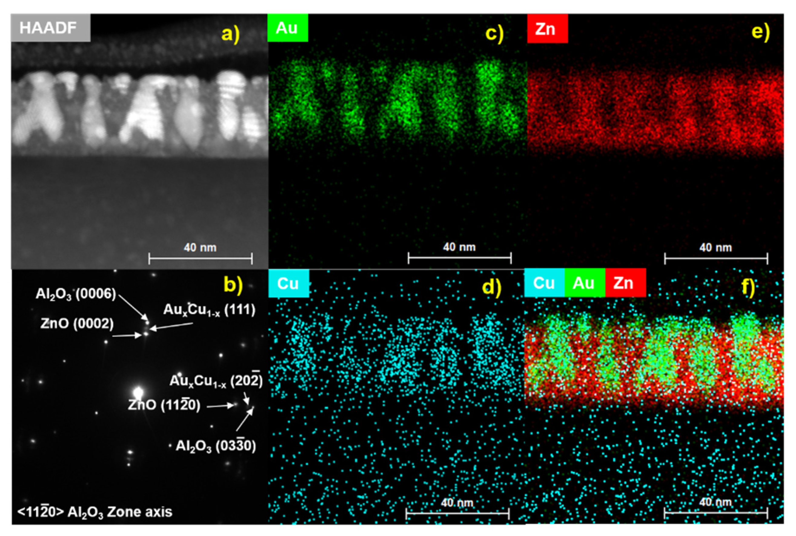
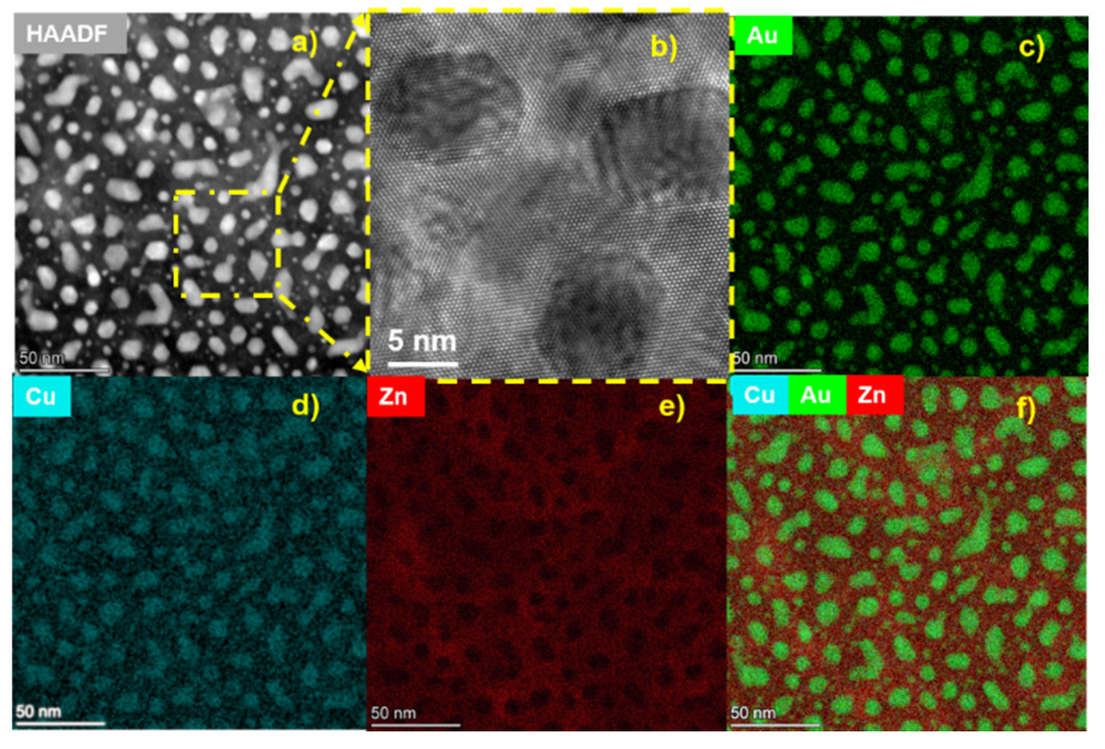
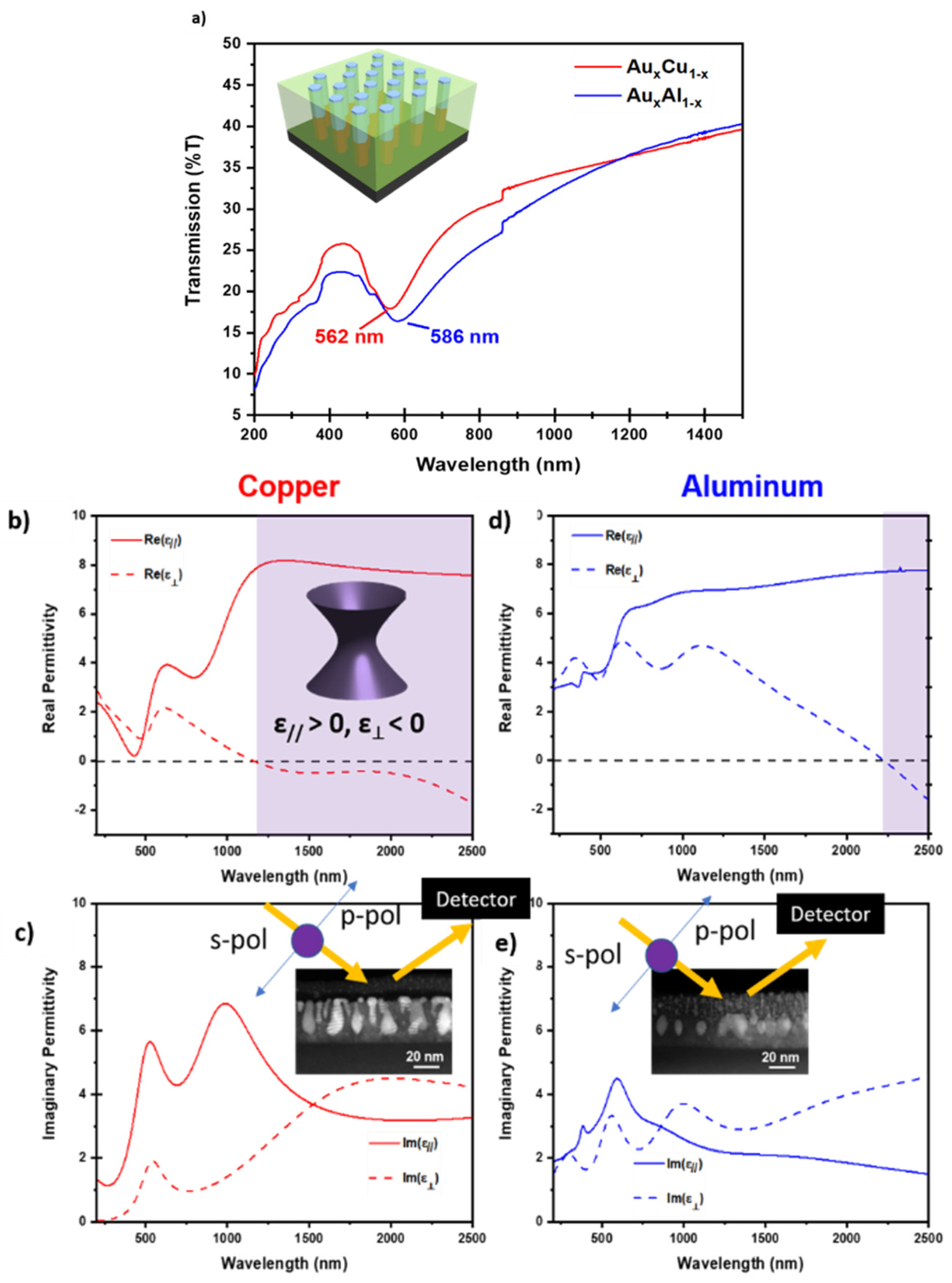
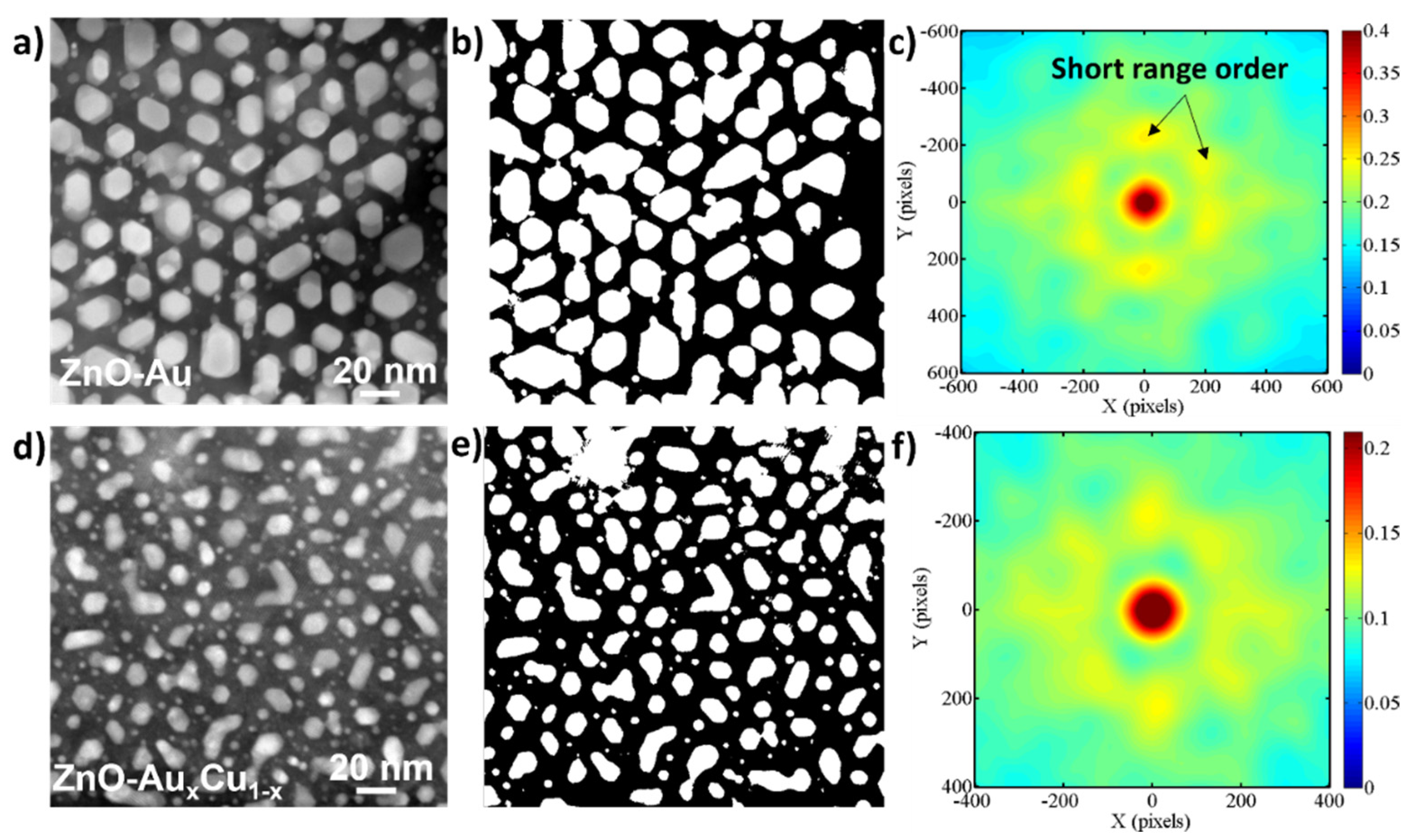
2. Results
3. Discussion
4. Materials and Methods
4.1. Thin-Film Growth
4.2. Microstructure Characterization
4.3. Optical Property Measurements
5. Conclusions
Supplementary Materials
Author Contributions
Funding
Institutional Review Board Statement
Informed Consent Statement
Data Availability Statement
Acknowledgments
Conflicts of Interest
Sample Availability
References
- Ferrari, L.; Wu, C.; Lepage, D.; Zhang, X.; Liu, Z. Hyperbolic metamaterials and their applications. Prog. Quantum Electron. 2015, 40, 1–40. [Google Scholar] [CrossRef]
- Poddubny, A.; Iorsh, I.; Belov, P.; Kivshar, Y. Hyperbolic metamaterials. Nat. Photonics 2013, 7, 958–967. [Google Scholar] [CrossRef]
- Yao, J.; Wang, Y.; Tsai, K.-T.; Liu, Z.; Yin, X.; Bartal, G.; Stacy, A.M.; Wang, Y.-L.; Zhang, X. Design, fabrication and characterization of indefinite metamaterials of nanowires. Philos. Trans. R. Soc. Lond. Ser. A Math. Phys. Eng. Sci. 2011, 369, 3434–3446. [Google Scholar] [CrossRef]
- Starko-Bowes, R.; Atkinson, J.; Newman, W.; Hu, H.; Kallos, T.; Palikaras, G.; Fedosejevs, R.; Pramanik, S.; Jacob, Z. Optical characterization of epsilon-near-zero, epsilon-near-pole, and hyperbolic response in nanowire metamaterials. J. Opt. Soc. Am. B 2015, 32, 2074–2080. [Google Scholar] [CrossRef] [Green Version]
- Noginov, M.A.; Barnakov, Y.A.; Zhu, G.; Tumkur, T.; Li, H.; Narimanov, E.E. Bulk photonic metamaterial with hyperbolic dispersion. Appl. Phys. Lett. 2009, 94, 151105. [Google Scholar] [CrossRef] [Green Version]
- Shi, Y.; Kim, H.K. Low-loss Plasmonic Metamaterial Waveguides. In Proceedings of the 2017 IEEE 17th International Conference on Nanotechnology (IEEE-NANO), Pittsburgh, PA, USA, 25–28 July 2017; pp. 890–893. [Google Scholar]
- Smolyaninova, V.N.; Jensen, C.; Zimmerman, W.; Prestigiacomo, J.C.; Osofsky, M.S.; Kim, H.; Bassim, N.; Xing, Z.; Qazilbash, M.M.; Smolyaninov, I.I. Enhanced superconductivity in aluminum-based hyperbolic metamaterials. Sci. Rep. 2016, 6, 34140. [Google Scholar] [CrossRef] [Green Version]
- Smolyaninov, I.I. Modeling of causality with metamaterials. J. Opt. 2013, 15, 1591–1595. [Google Scholar] [CrossRef] [Green Version]
- Smolyaninov, I.I.; Hwang, E.; Narimanov, E. Hyperbolic metamaterial interfaces: Hawking radiation from Rindler horizons and spacetime signature transitions. Phys. Rev. B Condens. Matter Mater. Phys. 2012, 85, 235122. [Google Scholar] [CrossRef] [Green Version]
- Sandrock, M.L.; Pibel, C.D.; Geiger, F.M.; Foss, C.A. Synthesis and Second-Harmonic Generation Studies of Noncentrosymmetric Gold Nanostructures. J. Phys. Chem. B 1999, 103, 2668–2673. [Google Scholar] [CrossRef]
- Zong, R.-L.; Zhou, J.; Li, Q.; Du, B.; Li, B.; Fu, M.; Qi, X.-W.; Li, L.-T.; Buddhudu, S. Synthesis and Optical Properties of Silver Nanowire Arrays Embedded in Anodic Alumina Membrane. J. Phys. Chem. B 2004, 108, 16713–16716. [Google Scholar] [CrossRef]
- Melosh, N.A.; Boukai, A.; Diana, F.; Gerardot, B.; Badolato, A.; Petroff, P.M.; Heath, J.R. Ultrahigh-density nanowire lattices and circuits. Science 2003, 300, 112–115. [Google Scholar] [CrossRef] [PubMed] [Green Version]
- Martin, J.; Plain, J. Fabrication of aluminium nanostructures for plasmonics. J. Phys. D Appl. Phys. 2015, 48, 184002. [Google Scholar] [CrossRef]
- Chan, G.H.; Zhao, J.; Hicks, E.M.; Schatz, G.C.; Van Duyne, R.P. Plasmonic Properties of Copper Nanoparticles Fabricated by Nanosphere Lithography. Nano Lett. 2007, 7, 1947–1952. [Google Scholar] [CrossRef]
- Li, L.; Sun, L.; Gomez-Diaz, J.S.; Hogan, N.L.; Lu, P.; Khatkhatay, F.; Zhang, W.; Jian, J.; Huang, J.; Su, Q.; et al. Self-Assembled Epitaxial Au–Oxide Vertically Aligned Nanocomposites for Nanoscale Metamaterials. Nano Lett. 2016, 16, 3936–3943. [Google Scholar] [CrossRef]
- MacManus-Driscoll, J.L.; Zerrer, P.; Wang, H.; Yang, H.; Yoon, J.; Fouchet, A.; Yu, R.; Blamire, M.; Jia, Q. Strain control and spontaneous phase ordering in vertical nanocomposite heteroepitaxial thin films. Nat. Mater. 2008, 7, 314–320. [Google Scholar] [CrossRef] [PubMed]
- Sun, X.; Li, Q.; Huang, J.; Fan, M.; Rutherford, B.X.; Paldi, R.L.; Jian, J.; Zhang, X.; Wang, H. Strain-driven nanodumbbell structure and enhanced physical properties in hybrid vertically aligned nanocomposite thin films. Appl. Mater. Today 2019, 16, 204–212. [Google Scholar] [CrossRef]
- Fan, M.; Zhang, B.; Wang, H.; Jian, J.; Sun, X.; Huang, J.; Li, L.; Zhang, X.; Wang, H. Self-Organized Epitaxial Vertically Aligned Nanocomposites with Long-Range Ordering Enabled by Substrate Nanotemplating. Adv. Mater. 2017, 29, 1606861. [Google Scholar] [CrossRef]
- Sun, X.; Kalaswad, M.; Li, Q.; Paldi, R.L.; Huang, J.; Wang, H.; Gao, X.; Zhang, X.; Wang, H. Role of Interlayer in 3D Vertically Aligned Nanocomposite Frameworks with Tunable Magnetotransport Properties. Adv. Mater. Interfaces 2020, 7, 1901990. [Google Scholar] [CrossRef]
- Paldi, R.L.; Qi, Z.; Misra, S.; Lu, J.; Sun, X.; Phuah, X.L.; Kalaswad, M.; Bischoff, J.; Branch, D.W.; Siddiqui, A.; et al. Nanocomposite-Seeded Epitaxial Growth of Single-Domain Lithium Niobate Thin Films for Surface Acoustic Wave Devices. Adv. Photonics Res. 2021, 2, 2000149. [Google Scholar] [CrossRef]
- Su, Q.; Zhang, W.; Lu, P.; Fang, S.; Khatkhatay, F.; Jian, J.; Li, L.; Chen, F.; Zhang, X.; MacManus-Driscoll, J.L.; et al. Self-Assembled Magnetic Metallic Nanopillars in Ceramic Matrix with Anisotropic Magnetic and Electrical Transport Properties. ACS Appl. Mater. Interfaces 2016, 8, 20283–20291. [Google Scholar] [CrossRef]
- Paldi, R.L.; Sun, X.; Wang, X.; Zhang, X.; Wang, H. Strain-Driven In-plane Ordering in Vertically Aligned ZnO-Au Nanocomposites with Highly Correlated Metamaterial Properties. ACS Omega 2020, 5, 2234–2241. [Google Scholar] [CrossRef] [PubMed] [Green Version]
- Huang, J.; Wang, X.; Phuah, X.; Lu, P.; Qi, Z.; Wang, H. Plasmonic Cu nanostructures in ZnO as hyperbolic metamaterial thin films. Mater. Today Nano 2019, 8, 100052. [Google Scholar] [CrossRef]
- Paldi, R.L.; Wang, X.; Sun, X.; He, Z.; Qi, Z.; Zhang, X.; Wang, H. Vertically Aligned AgxAu1−x Alloyed Nanopillars Embedded in ZnO as Nanoengineered Low-Loss Hybrid Plasmonic Metamaterials. Nano Lett. 2020, 20, 3778–3785. [Google Scholar] [CrossRef] [PubMed]
- Tomaev, V.V.; Polishchuk, V.A.; Vartanyan, T.A. Optical density of nanocomposite ZnO films doped with Au, Al, Cu. AIP Conf. Proc. 2019, 2064, 040006. [Google Scholar]
- Misra, S.; Zhang, D.; Lu, P.; Wang, H. Thermal stability of self-assembled ordered three-phase Au–BaTiO3–ZnO nanocomposite thin films via in situ heating in TEM. Nanoscale 2020, 12, 23673–23681. [Google Scholar] [CrossRef] [PubMed]
- Zhang, D.; Qi, Z.; Jian, J.; Huang, J.; Phuah, X.L.; Zhang, X.; Wang, H. Thermally Stable Au-BaTiO3 Nanoscale Hybrid Metamaterial for High-Temperature Plasmonic Applications. ACS Appl. Nano Mater. 2020, 3, 1431–1437. [Google Scholar] [CrossRef]
- Zhaoyang, W.; Lizhong, H. Effect of oxygen pressure on the structural and optical properties of ZnO thin films on Si (111) by PLD. Vacuum 2009, 83, 906–909. [Google Scholar] [CrossRef]
- Kumar, R.; Kumar, G.; Umar, A. Pulse Laser Deposited Nanostructured ZnO Thin Films: A Review. J. Nanosci. Nanotechnol. 2014, 14, 1911–1930. [Google Scholar] [CrossRef]
- Wang, X.; Jian, J.; Diaz-Amaya, S.; Kumah, C.E.; Lu, P.; Huang, J.; Lim, D.G.; Pol, V.G.; Youngblood, J.P.; Boltasseva, A.; et al. Hybrid plasmonic Au–TiN vertically aligned nanocomposites: A nanoscale platform towards tunable optical sensing. Nanoscale Adv. 2019, 1, 1045–1054. [Google Scholar] [CrossRef] [Green Version]
- Paldi, R.L.; Sun, X.; Phuah, X.L.; Lu, J.; Zhang, X.; Siddiqui, A.; Wang, H. Deposition pressure-induced microstructure control and plasmonic property tuning in hybrid ZnO–AgxAu1−x thin films. Nanoscale Adv. 2021, 3, 2870–2878. [Google Scholar] [CrossRef]
- Dahal, L.R.; Sainju, D.; Podraza, N.; Marsillac, S.; Collins, R. Real time spectroscopic ellipsometry of Ag/ZnO and Al/ZnO interfaces for back-reflectors in thin film Si:H photovoltaics. Thin Solid Films 2011, 519, 2682–2687. [Google Scholar] [CrossRef]
- Lu, L.; Simpson, R.E.; Valiyaveedu, S.K. Active hyperbolic metamaterials: Progress, materials and design. J. Opt. 2018, 20, 103001. [Google Scholar] [CrossRef]
- Fullwood, D.; Kalidindi, S.; Niezgoda, S.; Fast, A.; Hampson, N. Gradient-based microstructure reconstructions from distributions using fast Fourier transforms. Mater. Sci. Eng. A 2008, 494, 68–72. [Google Scholar] [CrossRef]
- Fullwood, D.T.; Niezgoda, S.; Kalidindi, S. Microstructure reconstructions from 2-point statistics using phase-recovery algorithms. Acta Mater. 2008, 56, 942–948. [Google Scholar] [CrossRef]
- Uklein, A.; Multian, V.; Kuz’Micheva, G.; Linnik, R.; Lisnyak, V.; Popov, A.; Gayvoronsky, V.Y. Nonlinear optical response of bulk ZnO crystals with different content of intrinsic defects. Opt. Mater. 2018, 84, 738–747. [Google Scholar] [CrossRef]

Publisher’s Note: MDPI stays neutral with regard to jurisdictional claims in published maps and institutional affiliations. |
© 2022 by the authors. Licensee MDPI, Basel, Switzerland. This article is an open access article distributed under the terms and conditions of the Creative Commons Attribution (CC BY) license (https://creativecommons.org/licenses/by/4.0/).
Share and Cite
Paldi, R.L.; Lu, J.; Pachaury, Y.; He, Z.; Bhatt, N.A.; Zhang, X.; El-Azab, A.; Siddiqui, A.; Wang, H. ZnO-AuxCu1−x Alloy and ZnO-AuxAl1−x Alloy Vertically Aligned Nanocomposites for Low-Loss Plasmonic Metamaterials. Molecules 2022, 27, 1785. https://doi.org/10.3390/molecules27061785
Paldi RL, Lu J, Pachaury Y, He Z, Bhatt NA, Zhang X, El-Azab A, Siddiqui A, Wang H. ZnO-AuxCu1−x Alloy and ZnO-AuxAl1−x Alloy Vertically Aligned Nanocomposites for Low-Loss Plasmonic Metamaterials. Molecules. 2022; 27(6):1785. https://doi.org/10.3390/molecules27061785
Chicago/Turabian StylePaldi, Robynne L., Juanjuan Lu, Yash Pachaury, Zihao He, Nirali A. Bhatt, Xinghang Zhang, Anter El-Azab, Aleem Siddiqui, and Haiyan Wang. 2022. "ZnO-AuxCu1−x Alloy and ZnO-AuxAl1−x Alloy Vertically Aligned Nanocomposites for Low-Loss Plasmonic Metamaterials" Molecules 27, no. 6: 1785. https://doi.org/10.3390/molecules27061785
APA StylePaldi, R. L., Lu, J., Pachaury, Y., He, Z., Bhatt, N. A., Zhang, X., El-Azab, A., Siddiqui, A., & Wang, H. (2022). ZnO-AuxCu1−x Alloy and ZnO-AuxAl1−x Alloy Vertically Aligned Nanocomposites for Low-Loss Plasmonic Metamaterials. Molecules, 27(6), 1785. https://doi.org/10.3390/molecules27061785