
Improvement in Optoelectronic Properties of Bismuth Sulphide Thin Films by Chromium Incorporation at the Orthorhombic Crystal Lattice for Photovoltaic Applications


 ,
,  ,
,
Abstract
:1. Introduction
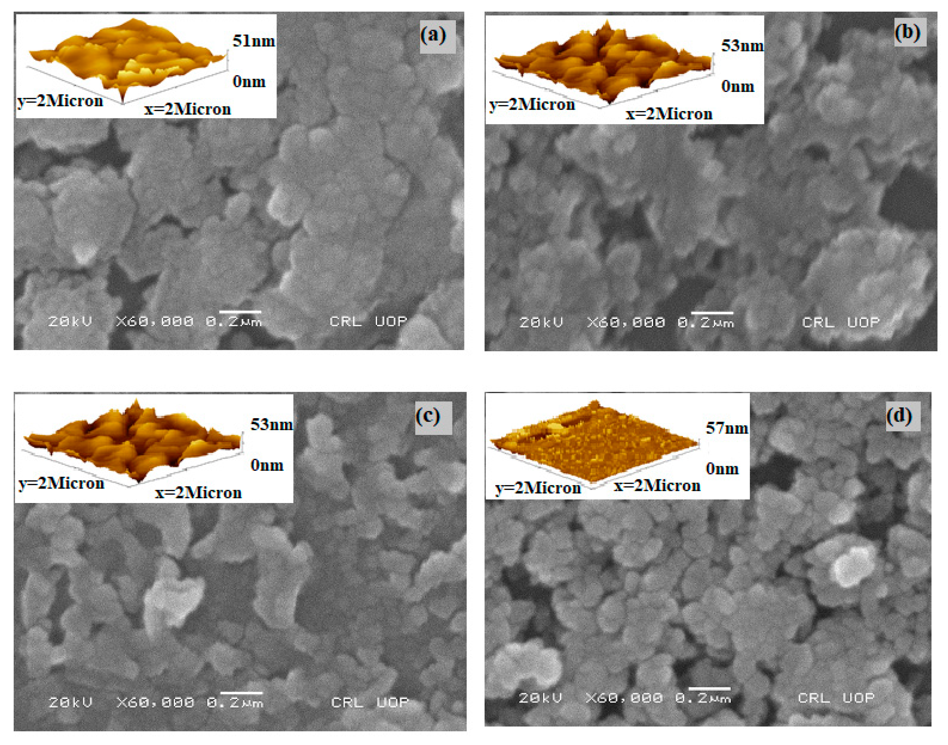
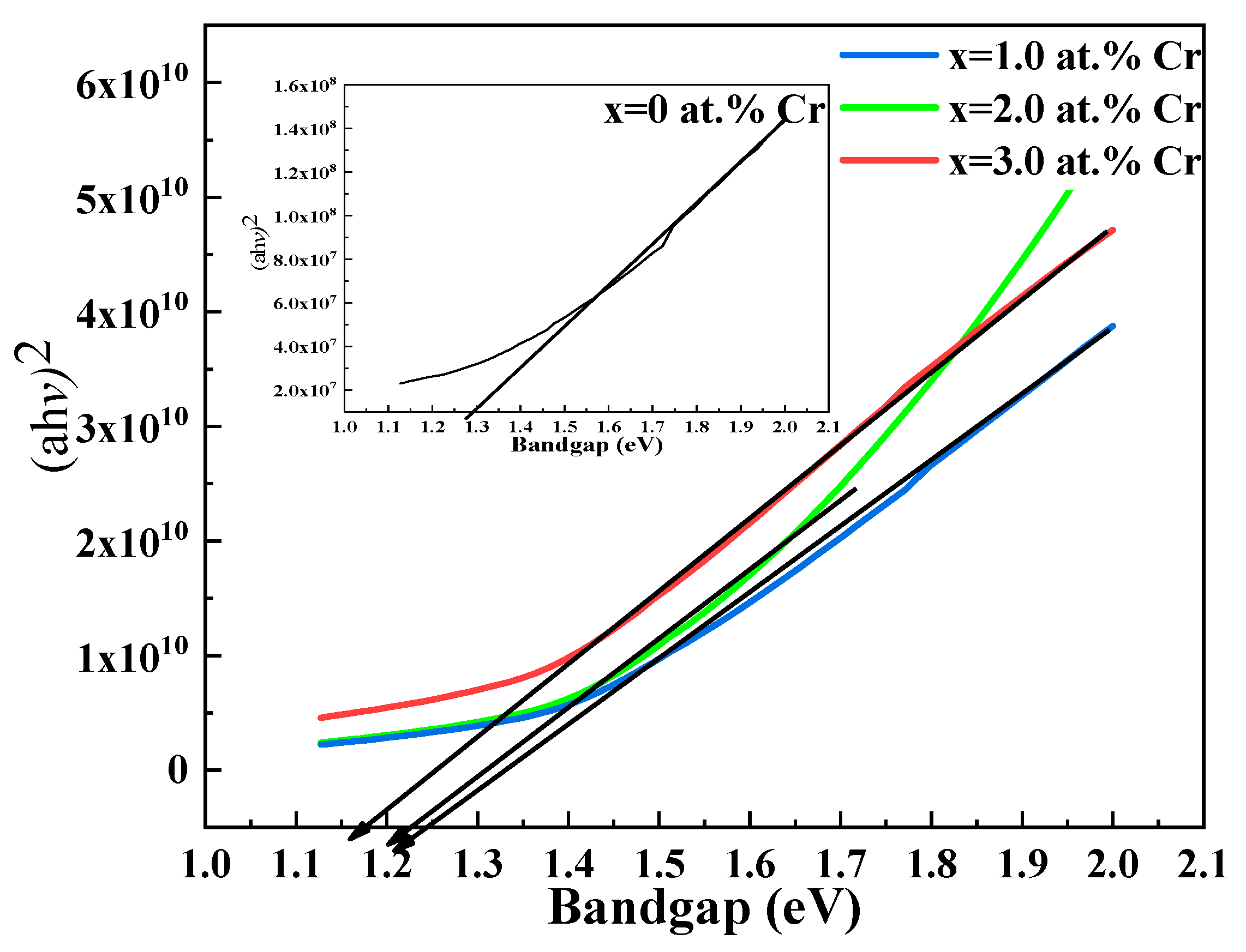
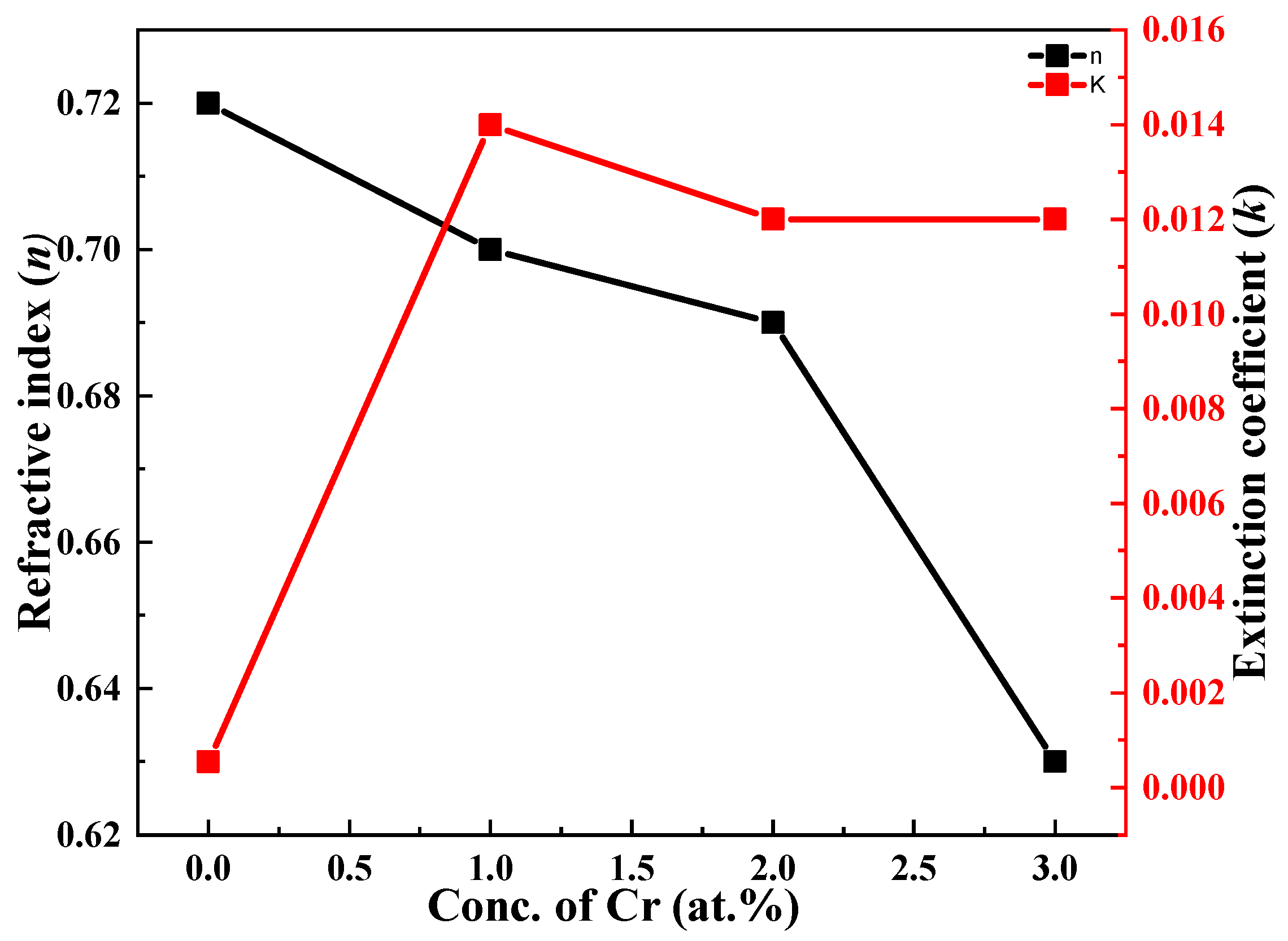
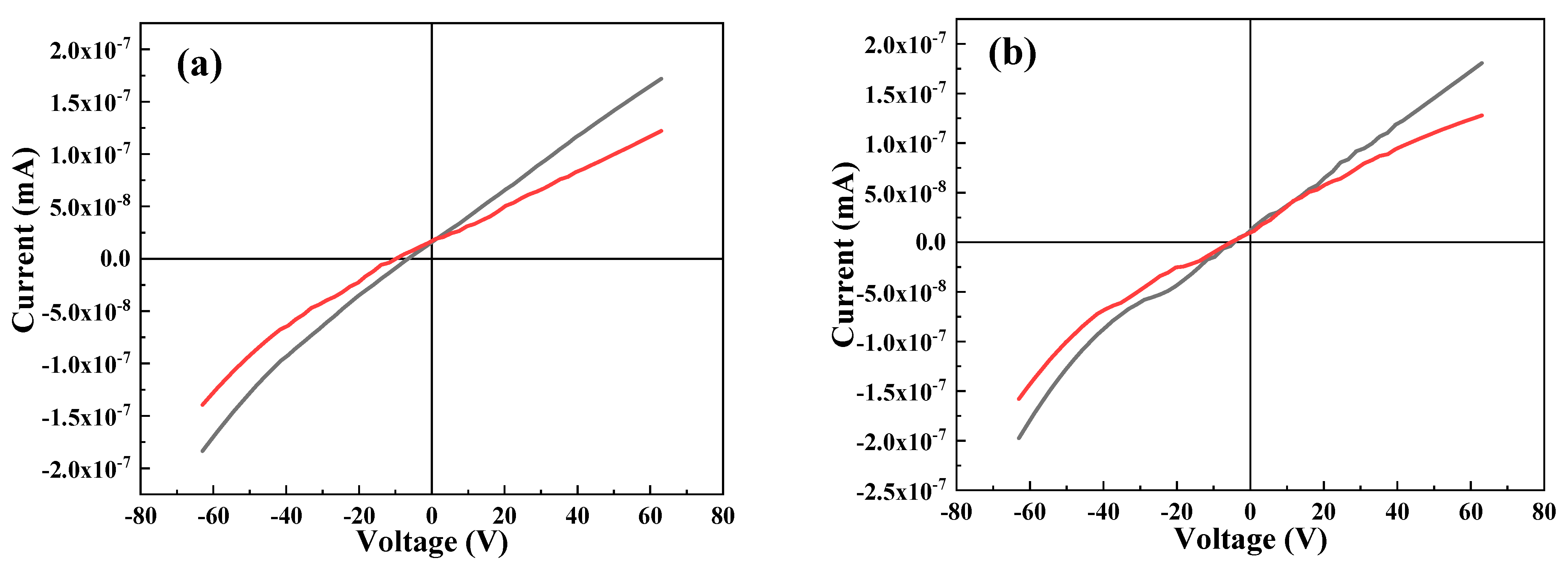
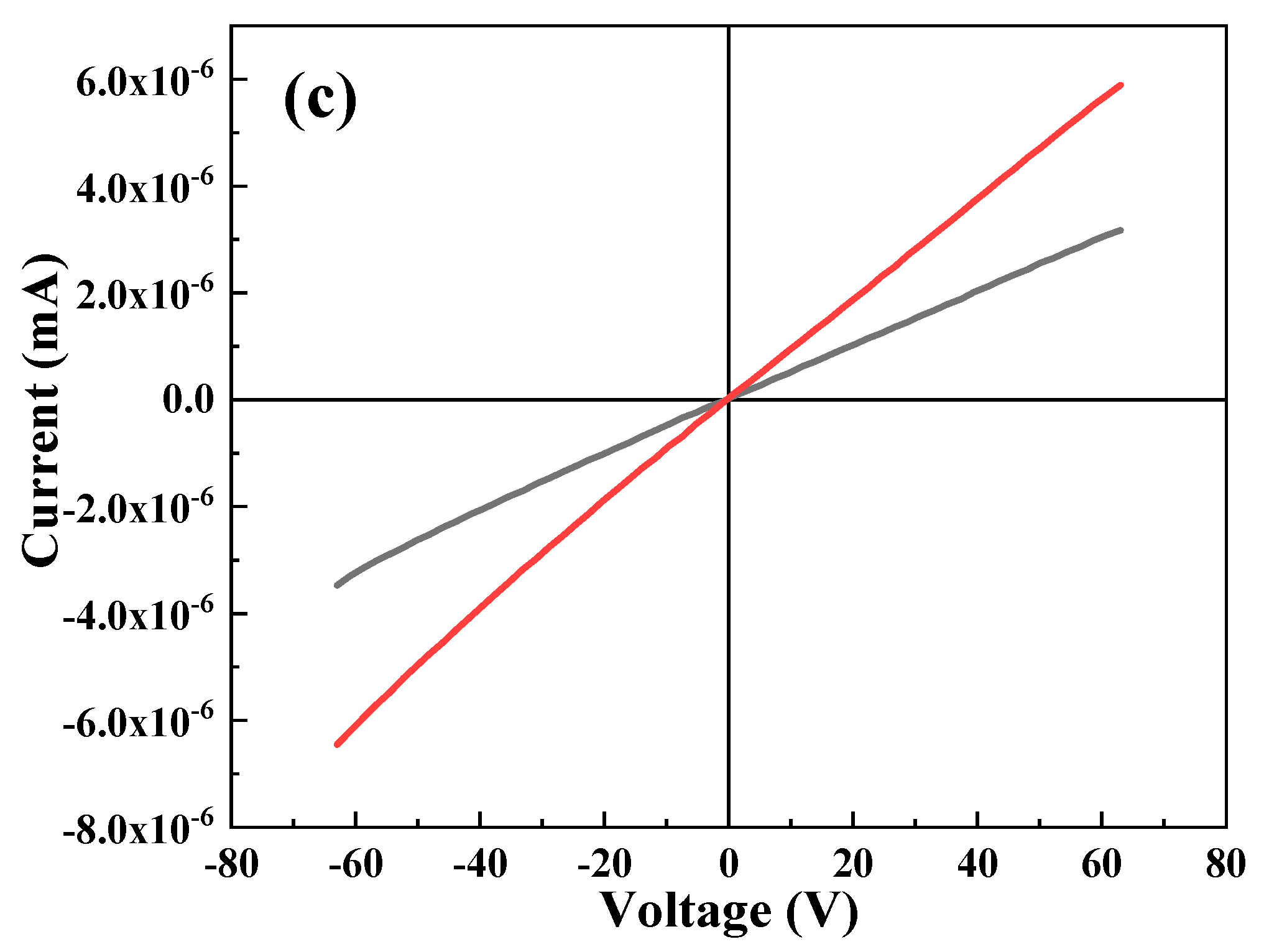
2. Results and Discussion
3. Materials and Methods
4. Conclusions
Author Contributions
Funding
Institutional Review Board Statement
Informed Consent Statement
Data Availability Statement
Acknowledgments
Conflicts of Interest
References
- Mohammed, M.K.; Shalan, A.E.; Dehghanipour, M.; Mohseni, H. Improved mixed-dimensional 3D/2D perovskite layer with formamidinium bromide salt for highly efficient and stable perovskite solar cells. Chem. Eng. J. 2022, 428, 131185. [Google Scholar] [CrossRef]
- Savill, K.J.; Ulatowski, A.M.; Herz, L.M. Optoelectronic Properties of Tin–Lead Halide Perovskites. ACS Energy Lett. 2021, 6, 2413–2426. [Google Scholar] [CrossRef] [PubMed]
- Schileo, G.; Grancini, G. Lead or no lead? Availability, toxicity, sustainability and environmental impact of lead-free perovskite solar cells. J. Mater. Chem. C 2021, 9, 67–76. [Google Scholar] [CrossRef]
- Gao, J.; Ma, X.; Xu, C.; Wang, X.; Son, J.H.; Jeong, S.Y.; Zhang, Y.; Zhang, C.; Wang, K.; Niu, L. Over 17.7% efficiency ternary-blend organic solar cells with low energy-loss and good thickness-tolerance. Chem. Eng. J. 2022, 428, 129276. [Google Scholar] [CrossRef]
- Salmanogli, A.; Gokcen, D. Entanglement Sustainability Improvement Using Optoelectronic Converter in Quantum Radar (Interferometric Object-Sensing). IEEE Sens. J. 2021, 21, 9054–9062. [Google Scholar] [CrossRef]
- Jafari, A.; Khademi, S.; Farahmandjou, M. Nano-crystalline Ce-doped TiO2 powders: Sol-gel synthesis and optoelectronic properties. Mater. Res. Express 2018, 5, 095008. [Google Scholar] [CrossRef]
- Thomas, K.J.; Singh, P.; Baheti, A.; Hsu, Y.-C.; Ho, K.-C.; Lin, J.T.s. Electro-optical properties of new anthracene based organic dyes for dye-sensitized solar cells. Dye. Pigment. 2011, 91, 33–43. [Google Scholar] [CrossRef]
- Wang, Y.; Li, T.; Chen, X.; Zhang, L. High-performance flexible lead-free perovskite solar cells based on tin-halide perovskite films doped by reductant metal halide. Mater. Lett. 2022, 321, 132460. [Google Scholar] [CrossRef]
- Zhang, P.; Xu, Y.; Tang, R.; Zhang, J.; Chen, K.; Liu, H.; Wu, F.; Zhong, C.; Liu, X.; Zhu, L. Periphery group engineering in hole transport materials for efficient perovskite solar cells. Dye. Pigment. 2022, 206, 110671. [Google Scholar] [CrossRef]
- Dou, J.; Bai, Y.; Chen, Q. Challenges of lead leakage in perovskite solar cells. Mater. Chem. Front. 2022, 6, 2779–2789. [Google Scholar] [CrossRef]
- Bhandari, S.; Mondal, D.; Nataraj, S.K.; Balakrishna, R.G. Biomolecule-derived quantum dots for sustainable optoelectronics. Nanoscale Adv. 2019, 1, 913–936. [Google Scholar] [CrossRef] [PubMed]
- Subramanian, A.; Azimi, M.; Santato, C.; Cicoira, F. Combining Aqueous Solution Processing and Printing for Fabrication of Flexible and Sustainable Tin Dioxide Ion-Gated Transistors. Adv. Mater. Techol. 2022, 7, 2100843. [Google Scholar] [CrossRef]
- Giraud, L.; Grelier, S.; Grau, E.; Hadziioannou, G.; Brochon, C.; Cramail, H.; Cloutet, E. Upgrading the chemistry of π-conjugated polymers toward more sustainable materials. J. Mater. Chem. C 2020, 8, 9792–9810. [Google Scholar] [CrossRef]
- Zhao, Y.; Wang, S.; Jiang, C.; Li, C.; Xiao, P.; Tang, R.; Gong, J.; Chen, G.; Chen, T.; Li, J. Regulating Energy Band Alignment via Alkaline Metal Fluoride Assisted Solution Post-Treatment Enabling Sb2(S,Se)3 Solar Cells with 10.7% Efficiency. Adv. Energy Mater. 2022, 12, 2103015. [Google Scholar] [CrossRef]
- Mustafa, G.M.; Zelai, T.; Bouzgarrou, S.; Alhossainy, M.; Mahmood, Q.; Mera, A.; Hegazy, H.; Alharthi, S.; Amin, M.A. First principle study of magnesium-based chalcogenides MgLa2(S/Se)4 for solar cells and renewable energy applications. Appl. Phys. A 2022, 128, 38. [Google Scholar] [CrossRef]
- Tao, K.; Tang, Y.; Rencus-Lazar, S.; Yao, Y.; Xue, B.; Gilead, S.; Wei, G.; Gazit, E. Bioinspired Supramolecular Packing Enables High Thermo-Sustainability. Angew. Chem. 2020, 59, 19037–19041. [Google Scholar] [CrossRef] [PubMed]
- Krueger, T.D.; Tang, L.; Giesbers, G.; Van Court, R.C.; Zhu, L.; Robinson, S.C.; Ostroverkhova, O.; Fang, C. Ultrafast Triplet State Formation in a Methylated Fungi-Derived Pigment: Toward Rational Molecular Design for Sustainable Optoelectronics. J. Phys. Chem. C 2021, 125, 17565–17572. [Google Scholar] [CrossRef]
- Rasal, A.S.; Chang, T.-W.; Korupalli, C.; Chang, J.-Y. Composition engineered ternary copper chalcogenide alloyed counter electrodes for high-performance and stable quantum dot-sensitized solar cells. Compos. Part B Eng. 2022, 232, 109610. [Google Scholar] [CrossRef]
- Guo, H.; Meng, R.; Wang, G.; Wang, S.; Wu, L.; Li, J.; Wang, Z.; Dong, J.; Hao, X.; Zhang, Y. Band-gap-graded Cu2ZnSn(S,Se)4 drives highly efficient solar cells. Energy Environ. Sci. 2022, 15, 693–704. [Google Scholar] [CrossRef]
- Sher, M.; Javed, M.; Shahid, S.; Iqbal, S.; Qamar, M.A.; Bahadur, A.; Qayyum, M.A. The controlled synthesis of g-C3N4/Cd-doped ZnO nanocomposites as potential photocatalysts for the disinfection and degradation of organic pollutants under visible light irradiation. RSC Adv. 2021, 11, 2025–2039. [Google Scholar] [CrossRef]
- Maria, C.C.S.; Patil, R.A.; Hasibuan, D.P.; Saragih, C.S.; Lai, C.-C.; Liou, Y.; Ma, Y.-R. White-light Photodetection Enhancement and Thin Film Impediment in Bi2S3 Nanorods/Thin-Films Homojunction Photodetectors. Appl. Surf. Sci. 2022, 584, 152608. [Google Scholar] [CrossRef]
- Pejova, B.; Grozdanov, I. Structural and optical properties of chemically deposited thin films of quantum-sized bismuth (III) sulfide. Mater. Chem. Phys. 2006, 99, 39–49. [Google Scholar] [CrossRef]
- Sakthivel, R.; Lin, L.-Y.; Lee, T.-H.; Liu, X.; He, J.-H.; Chung, R.-J. Disposable and cost-effective label-free electrochemical immunosensor for prolactin based on bismuth sulfide nanorods with polypyrrole. Bioelectrochemistry 2022, 143, 107948. [Google Scholar] [CrossRef] [PubMed]
- Ma, T.; Missous, M.; Pinter, G.; Zhong, X.; Spencer, B.; Thomas, A.G.; Lewis, D.J. Sustainable ITO films with reduced indium content deposited by AACVD. J. Mater. Chem. C 2022, 10, 579–589. [Google Scholar] [CrossRef]
- Anwar, S.; Anwar, S.; Mishra, B.K. Synthesis and Characterization of Bismuth Selenide Thin Films by Chemical Bath Deposition Technique. Adv. Sci. Lett. 2014, 20, 854–856. [Google Scholar] [CrossRef]
- Satoh, K.; Nakahara, A.; Mukunoki, K.; Sugiyama, H.; Saito, H.; Kamigaito, M. Sustainable cycloolefin polymer from pine tree oil for optoelectronics material: Living cationic polymerization of β-pinene and catalytic hydrogenation of high-molecular-weight hydrogenated poly(β-pinene). Polym. Chem. 2014, 5, 3222–3230. [Google Scholar] [CrossRef]
- Lagonegro, P.; Giovanella, U.; Pasini, M. Carbon Dots as a Sustainable New Platform for Organic Light Emitting Diode. Coatings 2021, 11, 5. [Google Scholar] [CrossRef]
- Azadmanjiri, J.; Kumar, P.; Srivastava, V.K.; Sofer, Z. Surface Functionalization of 2D Transition Metal Oxides and Dichalcogenides via Covalent and Non-covalent Bonding for Sustainable Energy and Biomedical Applications. ACS Appl. Nano Mater. 2020, 3, 3116–3143. [Google Scholar] [CrossRef]
- Jenisha, M.A.; Kavirajan, S.; Harish, S.; Archana, J.; Kamalabharathi, K.; Kumar, E.S.; Navaneethan, M. Interfacial engineering effect and bipolar conduction of Ni-doped MoS2 nanostructures for thermoelectric application. J. Alloys Compd. 2022, 895, 162493. [Google Scholar] [CrossRef]
- Fazal, T.; Iqbal, S.; Shah, M.; Bahadur, A.; Ismail, B.; Abd-Rabboh, H.S.M.; Hameed, R.; Mahmood, Q.; Ibrar, A.; Nasar, M.S.; et al. Deposition of bismuth sulfide and aluminum doped bismuth sulfide thin films for photovoltaic applications. J. Mater. Sci. Mater. Electron. 2022, 33, 42–53. [Google Scholar] [CrossRef]
- Iqbal, S.; Bahadur, A.; Anwer, S.; Ali, S.; Irfan, R.M.; Li, H.; Shoaib, M.; Raheel, M.; Anjum, T.A.; Zulqarnain, M.J.C.; et al. Effect of temperature and reaction time on the morphology of L-cysteine surface capped chalcocite (Cu2S) snowflakes dendrites nanoleaves and photodegradation study of methyl orange dye under visible light. Colloids Surf. A Physicochem. Eng. Asp. 2020, 601, 124984. [Google Scholar] [CrossRef]
- Tian, y.; Zhang, S.; Tan, W. Oxygen-doping to Bi2S3 thin film and its substrate-dependent resistive switching. Mater. Res. Express 2019, 6, 116324. [Google Scholar] [CrossRef]
- Hu, Z.; Deng, L.; Wu, T.; Wang, J.; Wu, F.; Chen, L.; Li, Q.; Liu, W.; Lien, S.-Y.; Gao, P. Compositional engineering of metal-xanthate precursors toward (Bi1−xSbx)2S3 (0 ≤ x ≤ 0.05) films with enhanced room temperature thermoelectric performance. J. Mater. Chem. C 2022. [Google Scholar] [CrossRef]
- Fazal, T.; Iqbal, S.; Shah, M.; Mahmood, Q.; Ismail, B.; Alsaab, H.O.; Awwad, N.S.; Ibrahium, H.A.; Elkaeed, E.B. Optoelectronic, structural and morphological analysis of Cu3BiS3 sulfosalt thin films. Results Phys. 2022, 36, 105453. [Google Scholar] [CrossRef]
- Fazal, T.; Iqbal, S.; Shah, M.; Mahmood, Q.; Ismail, B.; Alzhrani, R.M.; Awwad, N.S.; Ibrahium, H.A.; Alam, S.; Yasir, M.; et al. Optoelectronic Analysis of Bismuth Sulfide and Copper-Doped Bismuth Sulfide Thin Films. JOM 2022, 74, 2809–2816. [Google Scholar] [CrossRef]
- Green, M.A.; Emery, K.; Hishikawa, Y.; Warta, W.; Dunlop, E.D. Solar cell efficiency tables (Version 45). Prog. Photovolt. Res. Appl. 2015, 23, 1–9. [Google Scholar] [CrossRef]
- Resende, J.E.; Gonçalves, M.A.; Oliveira, L.C.A.; da Cunha, E.F.F.; Ramalho, T.C. Use of Ethylenediaminetetraacetic Acid as a Scavenger for Chromium from “Wet Blue” Leather Waste: Thermodynamic and Kinetics Parameters. J. Chem. 2014, 2014, 754526. [Google Scholar] [CrossRef]
- Song, Y.; Ammami, M.-T.; Benamar, A.; Mezazigh, S.; Wang, H. Effect of EDTA, EDDS, NTA and citric acid on electrokinetic remediation of As, Cd, Cr, Cu, Ni, Pb and Zn contaminated dredged marine sediment. Environ. Sci. Pollut. Res. 2016, 23, 10577–10586. [Google Scholar] [CrossRef]
- Smith, S.W. The role of chelation in the treatment of other metal poisonings. J. Med. Toxicol 2013, 9, 355–369. [Google Scholar] [CrossRef]
- Azizah, N.m.; Muhammady, S.; Purbayanto, M.A.K.; Nurfani, E.; Winata, T.; Sustini, E.; Widita, R.; Darma, Y. Influence of Al doping on the crystal structure, optical properties, and photodetecting performance of ZnO film. Prog. Nat. Sci. Mater. Int. 2020, 30, 28–34. [Google Scholar] [CrossRef]
- Ginting, M.; Taslima, S.; Sebayang, K.; Aryanto, D.; Sudiro, T.; Sebayang, P. Preparation and characterization of zinc oxide doped with ferrite and chromium. AIP Conf. Proc. 2017, 1826, 030062. [Google Scholar]
- Taziwa, R.; Meyer, E.; Katwire, D.; Ntozakhe, L. Influence of carbon modification on the morphological, structural, and optical properties of zinc oxide nanoparticles synthesized by pneumatic spray pyrolysis technique. J. Nanomater. 2017, 2017, 9095301. [Google Scholar] [CrossRef]
- Yilmaz, M.; Aydoğan, Ş. The effect of Pb doping on the characteristic properties of spin coated ZnO thin films: Wrinkle structures. Mater. Sci. Semicond. Process. 2015, 40, 162–170. [Google Scholar] [CrossRef]
- Sabarish, R.; Suriyanarayanan, N.; Kalita, J.M.; Sarma, M.P.; Wary, G. Investigation on growth, structural, optical, electrical and X-ray sensing properties of chemically deposited zinc bismuth sulfide (ZnxBi2−xS3) thin films. Mater. Res. Express 2018, 5, 056402. [Google Scholar] [CrossRef]
- Ahire, R.; Deshpande, N.; Gudage, Y.; Sagade, A.; Chavhan, S.; Phase, D.; Sharma, R. A comparative study of the physical properties of CdS, Bi2S3 and composite CdS–Bi2S3 thin films for photosensor application. Sens. Actuators A Phys. 2007, 140, 207–214. [Google Scholar] [CrossRef]
- Dai, J.; Jiang, X.; Wang, H.; Yan, D. Organic photovoltaic cells with near infrared absorption spectrum. Appl. Phys. Lett. 2007, 91, 253503. [Google Scholar] [CrossRef]
- Lewis, A.E. Review of metal sulphide precipitation. Hydrometallurgy 2010, 104, 222–234. [Google Scholar] [CrossRef]
- Desai, J.; Lokhande, C. Chemical deposition of Bi2S3 thin films from thioacetamide bath. Mater. Chem. Phys. 1995, 41, 98–103. [Google Scholar] [CrossRef]
- Salavati-Niasari, M.; Behfard, Z.; Amiri, O. Synthesis of bismuth sulfide nanostructures by using bismuth (III) monosalicylate precursor and fabrication of bismuth sulfide based p–n junction solar cells. Asia-Pac. J. Chem. Eng. 2014, 9, 16–23. [Google Scholar] [CrossRef]
- Mageshwari, K.; Sathyamoorthy, R. Nanocrystalline Bi2S3 thin films grown by thio-glycolic acid mediated successive ionic layer adsorption and reaction (SILAR) technique. Mater. Sci. Semicond. Process. 2013, 16, 43–50. [Google Scholar] [CrossRef]
- Moreno-García, H.; Messina, S.; Calixto-Rodriguez, M.; Martínez, H. Physical properties of chemically deposited Bi2S3 thin films using two post-deposition treatments. Appl. Surf. Sci. 2014, 311, 729–733. [Google Scholar] [CrossRef]
- Huang, L.; Nair, P.; Nair, M.; Zingaro, R.A.; Meyers, E.A. Chemical deposition of Bi2S3 thin films on glass substrates pretreated with organosilanes. Thin Solid Film. 1995, 268, 49–56. [Google Scholar] [CrossRef]
- Cabrita, J.; Ferreira, V.; Monteiro, O. Titanate nanofibers sensitized with nanocrystalline Bi2S3 as new electrocatalytic materials for ascorbic acid sensor applications. Electrochim. Acta 2014, 135, 121–127. [Google Scholar] [CrossRef]
- Tian, Y.; Zhang, S.; Tan, W. Improved optical and electrical switching in Bi2S3 nested nano-networks with broad trap distribution. Appl. Nanosci. 2022, 12, 2023–2030. [Google Scholar] [CrossRef]
- Xi, J.; Wang, H.; Zhang, B.; Hu, X.; Zhao, F.; Zeng, B. Type I Bi2S3@ZnS Core-shell Structured Photocatalyst for the Selective Photoelectrochemical Sensing of Cu2+. Anal. Methods 2019, 11, 2605–2610. [Google Scholar] [CrossRef]


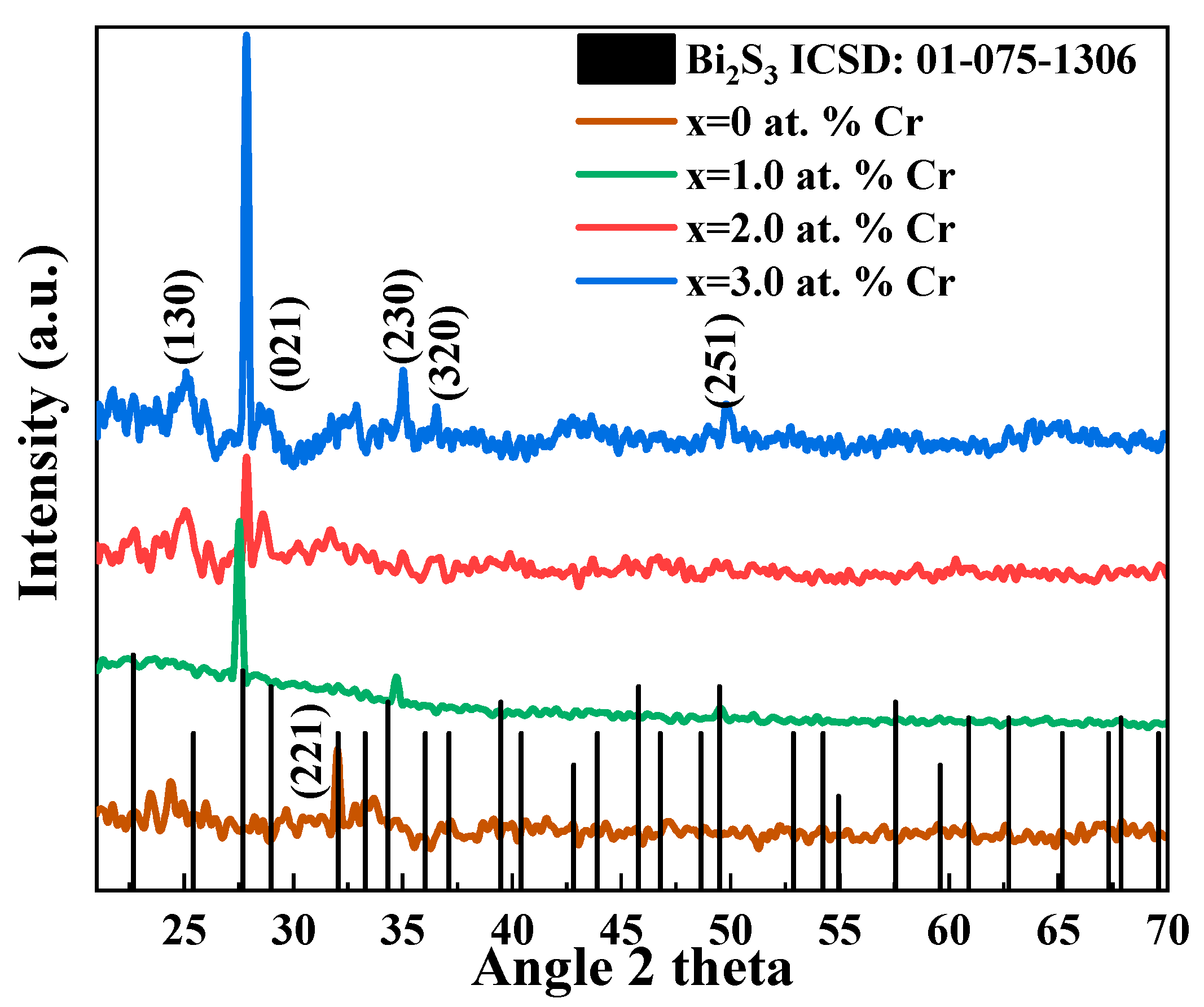
| Cr Conc. | Calculated Lattice Constant | Average Crystallite Size (nm) | X-ray Density (gcm−3) | Dislocation Density cm−2 | Average Microstrain × 10−3 | |||
|---|---|---|---|---|---|---|---|---|
| a (Å) 11.11 * | b (Å) 11.25 * | c (Å) 3.97 * | Volume of Cell (106 pm3) 496.42 * | |||||
| x = 0 | 11.11 | 11.71 | 3.52 | 457 | 141 | 7.4 | 2.1 | |
| x = 1 | 11.12 | 11.22 | 4.16 | 519 | 72 | 8.48 | 0.65 | 1.4 |
| x = 2 | 11.06 | 10.73 | 4.03 | 502 | 54 | 3.39 | 0.68 | 2.8 |
| x = 3 | 11.08 | 11.28 | 3.94 | 492 | 72 | 19.1 | 0.69 | 2.1 |
| Parameters | Conc. Of Cr (at.%) | |||
|---|---|---|---|---|
| 0 | 1.0 | 2.0 | 3.0 | |
| α × 104 (cm−1) | 80.90 | 333.9 | 315.59 | 319.30 |
| €i | 0.0008 | 0.0260 | 0.0238 | 0.0230 |
| €r | 0.5290 | 0.4896 | 0.4810 | 0.4828 |
| € | 0.5282 | 0.4638 | 0.00045 | 0.4595 |
| σe × 10 (Ω cm)−1 | 0.293 | 1.75 | 0.4517 | 1.64 |
| σo × 1015 (s−1) | 1.33 | 6.23 | 5.93 | 4.88 |
| σt × 10−4 (Ω cm/K) | 20 | 4 | 1.64 | 6.0 |
| Euo | 0.26 | 0.33 | 0.34 | 0.35 |
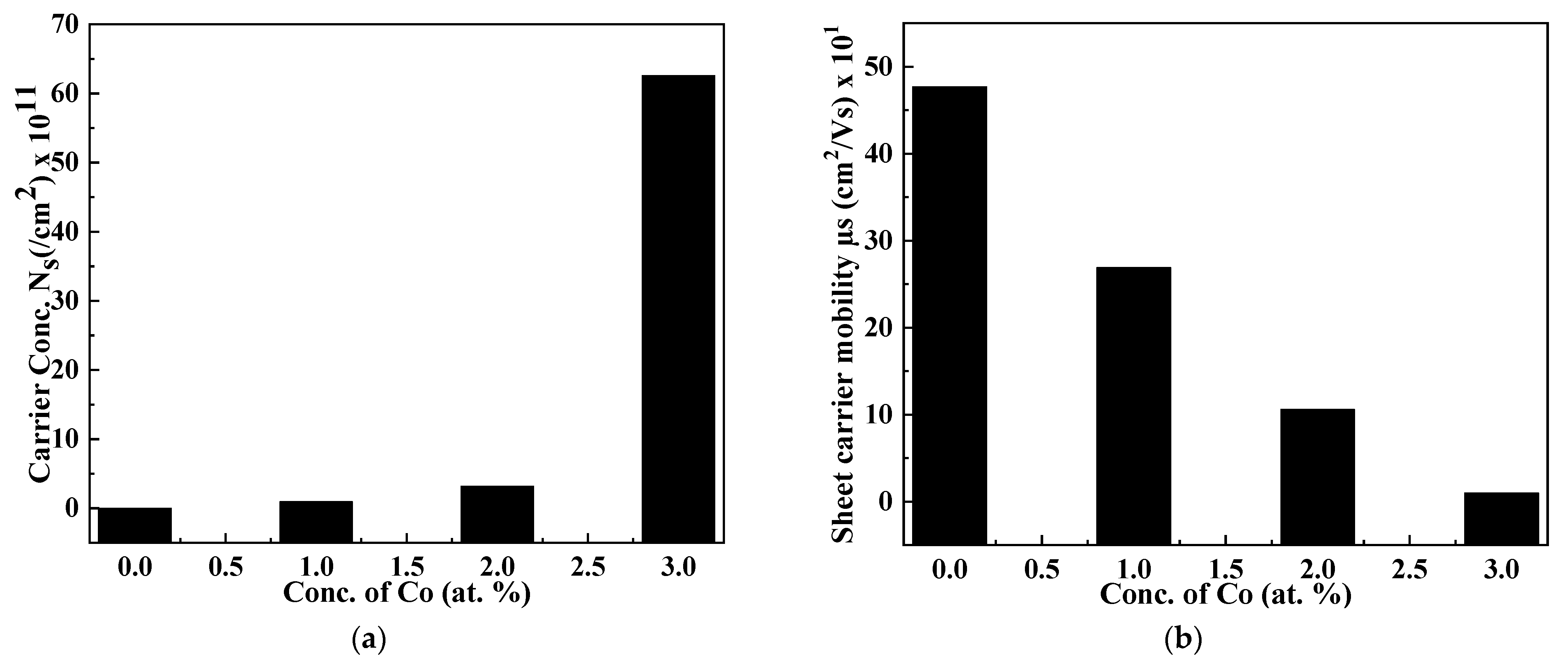
| Cr Conc (at.%) | I (µA) | Resistivity Rho (ohm cm) × 101 | Conductivity Con (1/ohm cm) × 10−2 | Carrier Concentration Ns (/cm2) × 1011 | Sheet Carrier Mobility µs (cm2/Vs) × 101 |
|---|---|---|---|---|---|
| 0 | 0.1 | 29.9 | 0.00393 | 0.016 | 47.7 |
| 1 | 0.1 | 21.2 | 2.14 | 0.950 | 26.9 |
| 2 | 0.1 | 6.48 | 2.12 | 3.19 | 10.6 |
| 3 | 0.1 | 5.90 | 1.54 | 62.6 | 1.01 |
Publisher’s Note: MDPI stays neutral with regard to jurisdictional claims in published maps and institutional affiliations. |
© 2022 by the authors. Licensee MDPI, Basel, Switzerland. This article is an open access article distributed under the terms and conditions of the Creative Commons Attribution (CC BY) license (https://creativecommons.org/licenses/by/4.0/).
Share and Cite
Fazal, T.; Iqbal, S.; Shah, M.; Ismail, B.; Shaheen, N.; Alrbyawi, H.; Al-Anazy, M.M.; Elkaeed, E.B.; Somaily, H.H.; Pashameah, R.A.; et al. Improvement in Optoelectronic Properties of Bismuth Sulphide Thin Films by Chromium Incorporation at the Orthorhombic Crystal Lattice for Photovoltaic Applications. Molecules 2022, 27, 6419. https://doi.org/10.3390/molecules27196419
Fazal T, Iqbal S, Shah M, Ismail B, Shaheen N, Alrbyawi H, Al-Anazy MM, Elkaeed EB, Somaily HH, Pashameah RA, et al. Improvement in Optoelectronic Properties of Bismuth Sulphide Thin Films by Chromium Incorporation at the Orthorhombic Crystal Lattice for Photovoltaic Applications. Molecules. 2022; 27(19):6419. https://doi.org/10.3390/molecules27196419
Chicago/Turabian StyleFazal, Tanzeela, Shahid Iqbal, Mazloom Shah, Bushra Ismail, Nusrat Shaheen, Hamad Alrbyawi, Murefah Mana Al-Anazy, Eslam B. Elkaeed, H. H. Somaily, Rami Adel Pashameah, and et al. 2022. "Improvement in Optoelectronic Properties of Bismuth Sulphide Thin Films by Chromium Incorporation at the Orthorhombic Crystal Lattice for Photovoltaic Applications" Molecules 27, no. 19: 6419. https://doi.org/10.3390/molecules27196419
APA StyleFazal, T., Iqbal, S., Shah, M., Ismail, B., Shaheen, N., Alrbyawi, H., Al-Anazy, M. M., Elkaeed, E. B., Somaily, H. H., Pashameah, R. A., Alzahrani, E., & Farouk, A.-E. (2022). Improvement in Optoelectronic Properties of Bismuth Sulphide Thin Films by Chromium Incorporation at the Orthorhombic Crystal Lattice for Photovoltaic Applications. Molecules, 27(19), 6419. https://doi.org/10.3390/molecules27196419