
Highly Efficient Reproducible Perovskite Solar Cells Prepared by Low-Temperature Processing


Abstract
:
1. Introduction
2. Results
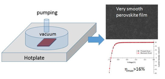
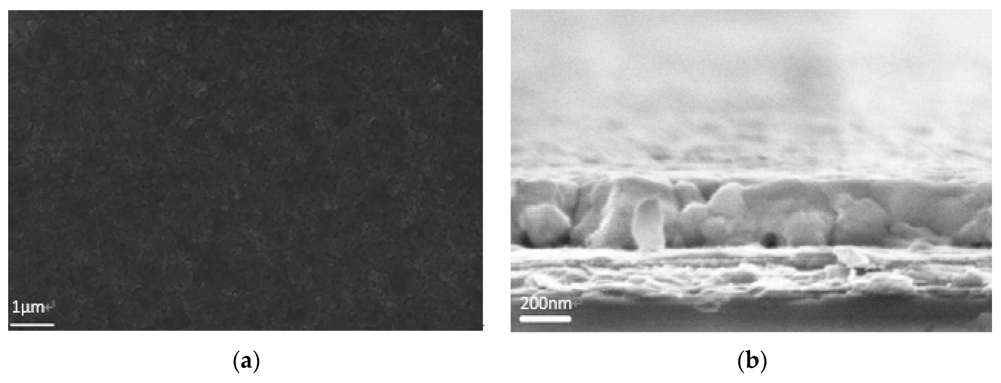
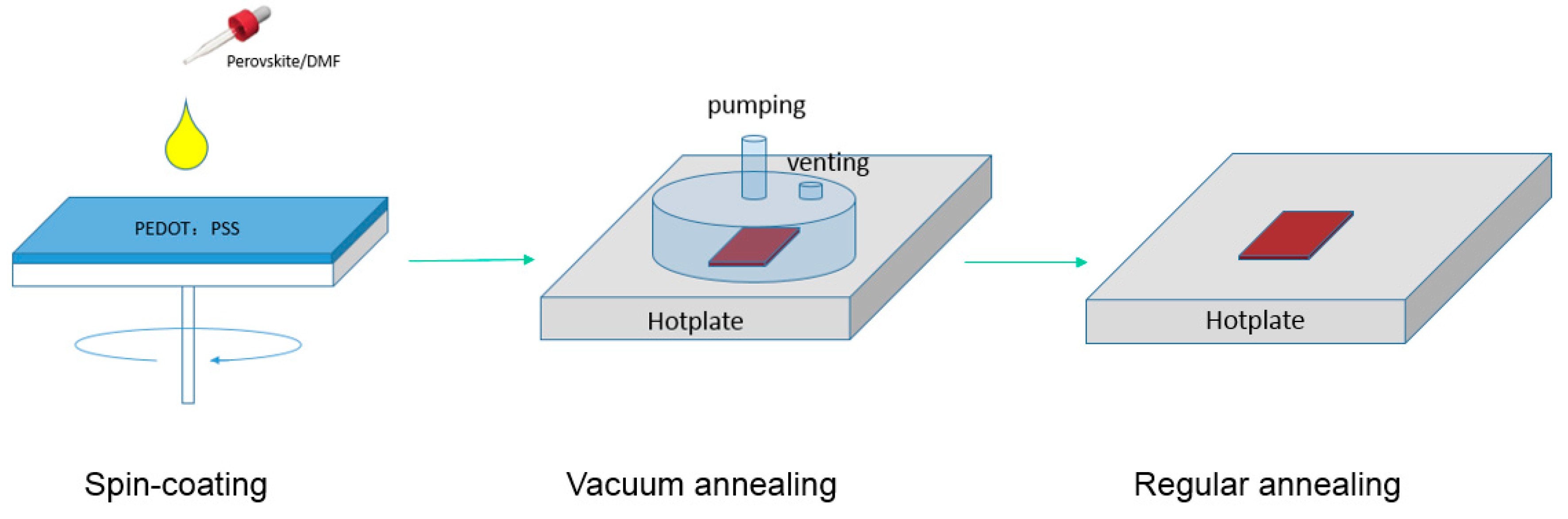
2.1. Perovskite Layer
2.2. C60 Layer
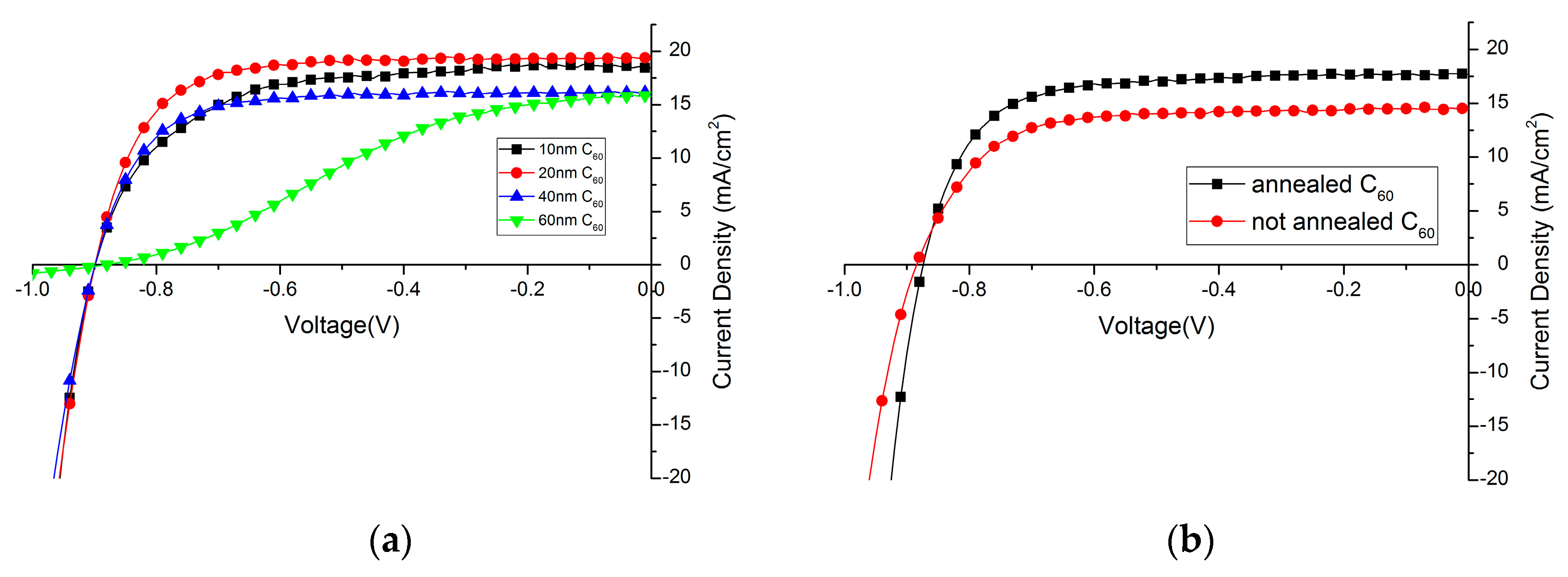
2.2.1. Influence of C60 Layer Thickness
2.2.2. Influence of C60 Annealing
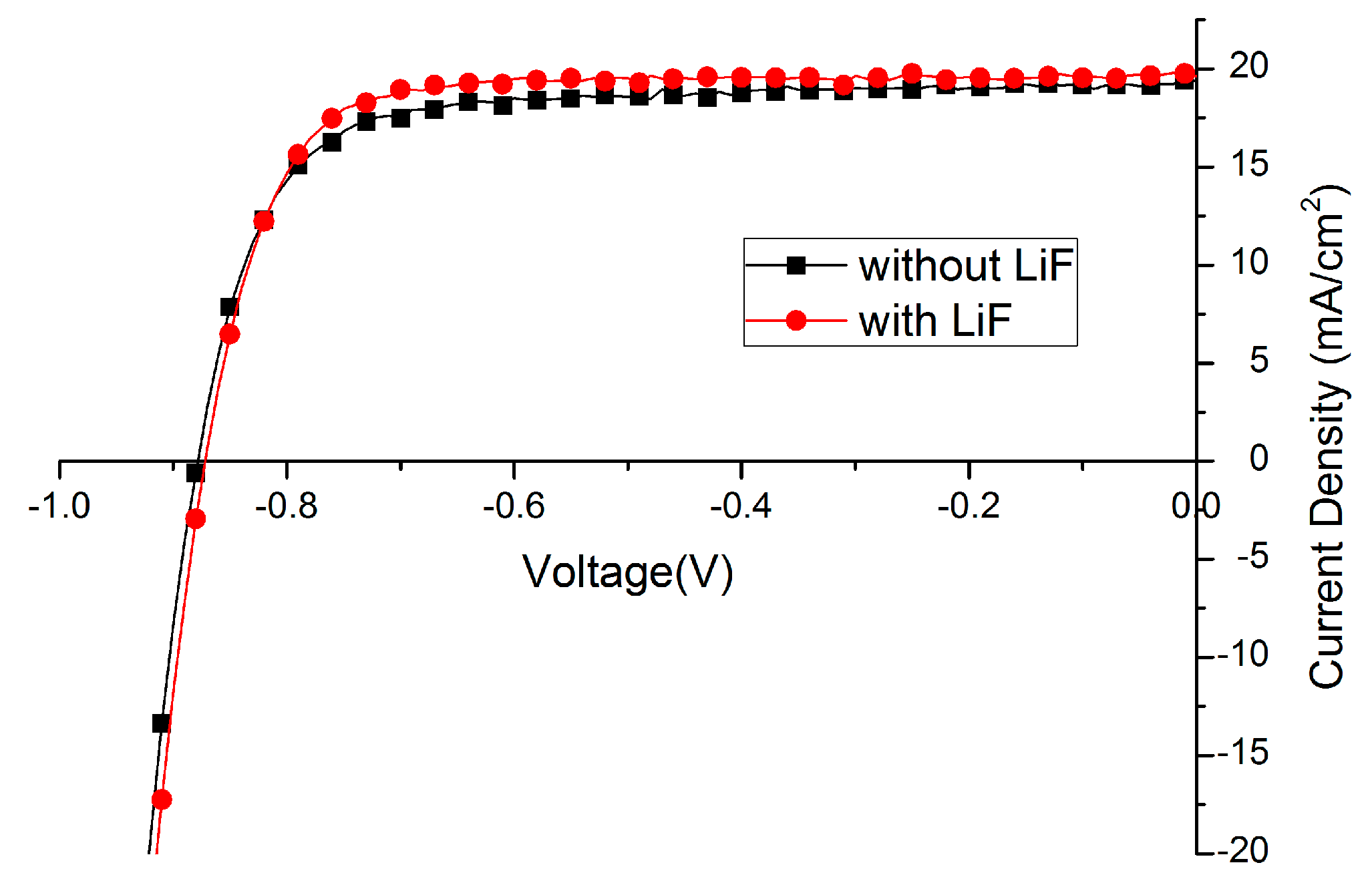
2.3. Further Optimization
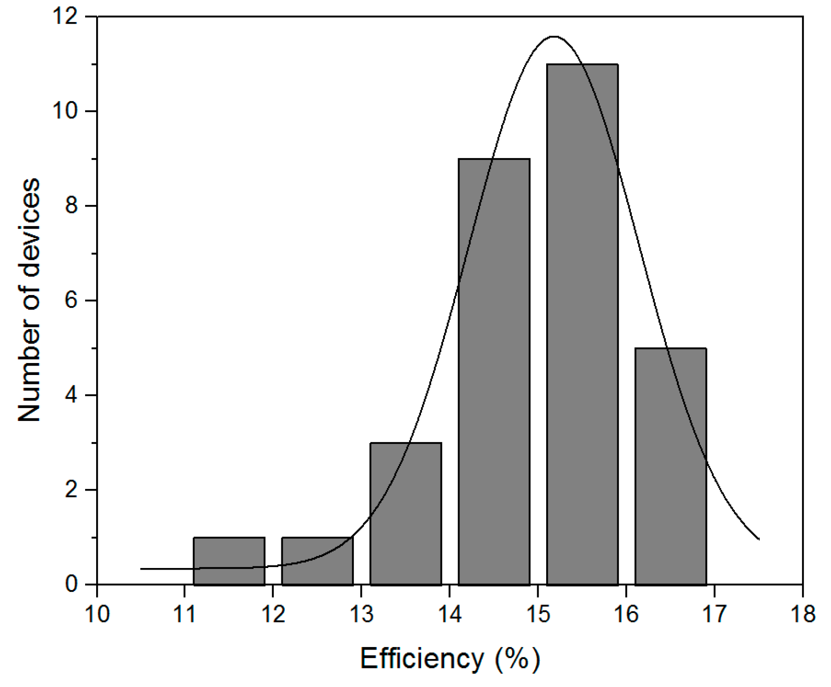
2.4. Optimized Solar Cell Performance and Statistical Results
3. Discussion
4. Materials and Methods
4.1. Preparation of the Precursor
4.2. Fabrication of the Devices
4.3. Device Characterization
Supplementary Materials
Acknowledgments
Author Contributions
Conflicts of Interest
References
- Kojima, A.; Teshima, K.; Shirai, Y.; Miyasaka, T. Organometal Halide Perovskites as Visible-Light Sensitizers for Photovoltaic Cells. J. Am. Chem. Soc. 2009, 131, 6050–6051. [Google Scholar] [CrossRef] [PubMed]
- Yang, W.S.; Noh, J.H.; Jeon, N.J.; Kim, Y.C.; Ryu, S.; Seo, J.; Seok, S.I. High-performance photovoltaic perovskite layers fabricated through intramolecular exchange. Science 2015, 348, 1234–1237. [Google Scholar] [CrossRef] [PubMed]
- Jeon, N.J.; Noh, J.H.; Yang, W.S.; Kim, Y.C.; Ryu, S.; Seo, J.; Seok, S.I. Compositional engineering of perovskite materials for high-performance solar cells. Nature 2015, 517, 476–480. [Google Scholar] [CrossRef] [PubMed]
- Walsh, A. Principles of Chemical Bonding and Band Gap Engineering in Hybrid Organic-Inorganic Halide Perovskites. J. Phys. Chem. C 2015, 119, 5755–5760. [Google Scholar] [CrossRef] [PubMed]
- Noh, J.H.; Im, S.H.; Heo, J.H.; Mandal, T.N.; Seok, S.I. Chemical Management for Colorful, Efficient, and Stable Inorganic-Organic Hybrid Nanostructured Solar Cells. Nano Lett. 2013, 13, 1764–1769. [Google Scholar] [CrossRef] [PubMed]
- Kulkarni, S.A.; Baikie, T.; Boix, P.P.; Yantara, N.; Mathews, N.; Mhaisalkar, S. Band-gap tuning of lead halide perovskites using a sequential deposition process. J. Mater. Chem. A 2014, 2, 9221–9225. [Google Scholar] [CrossRef]
- D’Innocenzo, V.; Srimath Kandada, A.R.; De Bastiani, M.; Gandini, M.; Petrozza, A. Tuning the Light Emission Properties by Band Gap Engineering in Hybrid Lead Halide Perovskite. J. Am. Chem. Soc. 2014, 136, 17730–17733. [Google Scholar] [CrossRef] [PubMed]
- De Wolf, S.; Holovsky, J.; Moon, S.-J.; Löper, P.; Niesen, B.; Ledinsky, M.; Haug, F.-J.; Yum, J.-H.; Ballif, C. Organometallic Halide Perovskites: Sharp Optical Absorption Edge and its Relation to Photovoltaic Performance. J. Phys. Chem. Lett. 2014, 5, 1035–1039. [Google Scholar] [CrossRef] [PubMed]
- Zhu, X.; Su, H.; Marcus, R.A.; Michel-Beyerle, M.E. Computed and Experimental Absorption Spectra of the Perovskite CH3NH3PbI3. J. Phys. Chem. Lett. 2014, 5, 3061–3065. [Google Scholar] [CrossRef] [PubMed]
- Dong, Q.; Fang, Y.; Shao, Y.; Mulligan, P.; Qiu, J.; Cao, L.; Huang, J. Electron-hole diffusion lengths > 175 µm in solution-grown CH3NH3PbI3 single crystals. Science 2015, 347, 967–970. [Google Scholar] [CrossRef] [PubMed]
- Shi, D.; Adinolfi, V.; Comin, R.; Yuan, M.; Alarousu, E.; Buin, A.; Chen, Y.; Hoogland, S.; Rothenberger, A.; Katsiev, K.; et al. Low trap-state density and long carrier diffusion in organolead trihalide perovskite single crystals. Science 2015, 347, 519–522. [Google Scholar] [CrossRef] [PubMed]
- Stranks, S.D.; Eperon, G.E.; Grancini, G.; Menelaou, C.; Alcocer, M.J.P.; Leijtens, T.; Herz, L.M.; Petrozza, A.; Snaith, H.J. Electron-Hole Diffusion Lengths Exceeding 1 Micrometer in an Organometal Trihalide Perovskite Absorber. Science 2013, 342, 341–344. [Google Scholar] [CrossRef] [PubMed]
- Xing, G.; Mathews, N.; Sun, S.; Lim, S.S.; Lam, Y.M.; Gratzel, M.; Mhaisalkar, S.; Sum, T.C. Long-Range Balanced Electron- and Hole-Transport Lengths in Organic-Inorganic CH3NH3PbI3. Science 2013, 342, 344–347. [Google Scholar] [CrossRef] [PubMed]
- Im, J.H.; Lee, C.R.; Lee, J.W.; Park, S.W.; Park, N.G. 6.5% efficient perovskite quantum-dot-sensitized solar cell. Nanoscale 2011, 3, 4088–4093. [Google Scholar] [CrossRef] [PubMed]
- Etgar, L.; Gao, P.; Xue, Z.S.; Peng, Q.; Chandiran, A.K.; Liu, B.; Nazeeruddin, M.K.; Gratzel, M. Mesoscopic CH3NH3PbI3/TiO2 Heterojunction Solar Cells. J. Am. Chem. Soc. 2012, 134, 17396–17399. [Google Scholar] [CrossRef] [PubMed]
- Kim, H.S.; Lee, C.R.; Im, J.H.; Lee, K.B.; Moehl, T.; Marchioro, A.; Moon, S.J.; Humphry-Baker, R.; Yum, J.H.; Moser, J.E.; et al. Lead Iodide Perovskite Sensitized All-Solid-State Submicron Thin Film Mesoscopic Solar Cell with Efficiency Exceeding 9%. Sci. Rep. 2012, 2, 591. [Google Scholar] [CrossRef] [PubMed]
- Zhou, H.; Chen, Q.; Li, G.; Luo, S.; Song, T.-B.; Duan, H.-S.; Hong, Z.; You, J.; Liu, Y.; Yang, Y. Interface engineering of highly efficient perovskite solar cells. Science 2014, 345, 542–546. [Google Scholar] [CrossRef] [PubMed]
- Chen, Q.; Zhou, H.; Hong, Z.; Luo, S.; Duan, H.-S.; Wang, H.-H.; Liu, Y.; Li, G.; Yang, Y. Planar heterojunction perovskite solar cells via vapor assisted solution process. J. Am. Chem. Soc. 2013, 136, 622–625. [Google Scholar] [CrossRef] [PubMed]
- Liu, M.; Johnston, M.B.; Snaith, H.J. Efficient planar heterojunction perovskite solar cells by vapour deposition. Nature 2013, 501, 395–398. [Google Scholar] [CrossRef] [PubMed]
- Kim, H.-S.; Park, N.-G. Parameters Affecting I–V Hysteresis of CH3NH3PbI3 Perovskite Solar Cells: Effects of Perovskite Crystal Size and Mesoporous TiO2 Layer. J. Phys. Chem. Lett. 2014, 5, 2927–2934. [Google Scholar] [CrossRef] [PubMed]
- Shao, Y.H.; Xiao, Z.G.; Bi, C.; Yuan, Y.B.; Huang, J.S. Origin and elimination of photocurrent hysteresis by fullerene passivation in CH3NH3PbI3 planar heterojunction solar cells. Nat. Commun. 2014, 5, 5784. [Google Scholar] [CrossRef] [PubMed]
- Heo, J.H.; You, M.S.; Chang, M.H.; Yin, W.; Ahn, T.K.; Lee, S.-J.; Sung, S.-J.; Kim, D.H.; Im, S.H. Hysteresis-less mesoscopic CH3NH3PbI3 perovskite hybrid solar cells by introduction of Li-treated TiO2 electrode. Nano Energy 2015, 15, 530–539. [Google Scholar] [CrossRef]
- Jena, A.K.; Chen, H.-W.; Kogo, A.; Sanehira, Y.; Ikegami, M.; Miyasaka, T. The Interface between FTO and the TiO2 Compact Layer Can Be One of the Origins to Hysteresis in Planar Heterojunction Perovskite Solar Cells. ACS Appl. Mater. Interfaces 2015, 7, 9817–9823. [Google Scholar] [CrossRef] [PubMed]
- Docampo, P.; Ball, J.M.; Darwich, M.; Eperon, G.E.; Snaith, H.J. Efficient organometal trihalide perovskite planar-heterojunction solar cells on flexible polymer substrates. Nat. Commun. 2013, 4, 2761. [Google Scholar] [CrossRef] [PubMed]
- Forgacs, D.; Sessolo, M.; Bolink, H.J. Lead acetate precursor based p-i-n perovskite solar cells with enhanced reproducibility and low hysteresis. J. Mater. Chem. A 2015, 3, 14121–14125. [Google Scholar] [CrossRef]
- Heo, J.H.; Han, H.J.; Kim, D.; Ahn, T.K.; Im, S.H. Hysteresis-less inverted CH3NH3PbI3 planar perovskite hybrid solar cells with 18.1% power conversion efficiency. Energy Environ. Sci. 2015, 8, 1602–1608. [Google Scholar] [CrossRef]
- Wu, C.-G.; Chiang, C.-H.; Tseng, Z.-L.; Nazeeruddin, M.K.; Hagfeldt, A.; Gratzel, M. High efficiency stable inverted perovskite solar cells without current hysteresis. Energy Environ. Sci. 2015, 8, 2725–2733. [Google Scholar] [CrossRef]
- Heo, J.H.; Im, S.H. Highly reproducible, efficient hysteresis-less CH3NH3PbI3-xClx planar hybrid solar cells without requiring heat-treatment. Nanoscale 2016, 8, 2554–2560. [Google Scholar] [CrossRef] [PubMed]
- El-Henawey, M.I.; Gebhardt, R.S.; El-Tonsy, M.M.; Chaudhary, S. Organic solvent vapor treatment of lead iodide layers in the two-step sequential deposition of CH3NH3PbI3-based perovskite solar cells. J. Mater. Chem. A 2016, 4, 1947–1952. [Google Scholar] [CrossRef]
- Chiang, C.-H.; Tseng, Z.-L.; Wu, C.-G. Planar heterojunction perovskite/PC71BM solar cells with enhanced open-circuit voltage via a (2/1)-step spin-coating process. J. Mater. Chem. A 2014, 2, 15897–15903. [Google Scholar] [CrossRef]
- Chiang, Y.-F.; Jeng, J.-Y.; Lee, M.-H.; Peng, S.-R.; Chen, P.; Guo, T.-F.; Wen, T.-C.; Hsu, Y.-J.; Hsu, C.-M. High voltage and efficient bilayer heterojunction solar cells based on an organic-inorganic hybrid perovskite absorber with a low-cost flexible substrate. Phys. Chem. Chem. Phys. 2014, 16, 6033–6040. [Google Scholar] [CrossRef] [PubMed]
- Jeng, J.Y.; Chen, K.C.; Chiang, T.Y.; Lin, P.Y.; Tsai, T.D.; Chang, Y.C.; Guo, T.F.; Chen, P.; Wen, T.C.; Hsu, Y.J. Nickel oxide electrode interlayer in CH3NH3PbI3 perovskite/PCBM planar-heterojunction hybrid solar cells. Adv. Mater. 2014, 26, 4107–4113. [Google Scholar] [CrossRef] [PubMed]
- Jeng, J.Y.; Chiang, Y.F.; Lee, M.H.; Peng, S.R.; Guo, T.F.; Chen, P.; Wen, T.C. CH3NH3PbI3 Perovskite/Fullerene Planar-Heterojunction Hybrid Solar Cells. Adv. Mater. 2013, 25, 3727–3732. [Google Scholar] [CrossRef] [PubMed]
- Seo, J.; Park, S.; Chan Kim, Y.; Jeon, N.J.; Noh, J.H.; Yoon, S.C.; Seok, S.I. Benefits of very thin PCBM and LiF layers for solution-processed p-i-n perovskite solar cells. Energy Environ. Sci. 2014, 7, 2642–2646. [Google Scholar] [CrossRef]
- Even, J.; Pedesseau, L.; Katan, C.; Kepenekian, M.; Lauret, J.-S.; Sapori, D.; Deleporte, E. A Solid State Physics Perspective on Hybrid Perovskite Semiconductors. J. Phys. Chem. C 2015, 119, 10161–10177. [Google Scholar] [CrossRef]
- Gong, X.; Li, M.; Shi, X.-B.; Ma, H.; Wang, Z.-K.; Liao, L.-S. Controllable Perovskite Crystallization by Water Additive for High-Performance Solar Cells. Adv. Funct. Mater. 2015, 25, 6671–6678. [Google Scholar] [CrossRef]
- Chiang, C.-H.; Wu, C.-G. Bulk heterojunction perovskite–PCBM solar cells with high fill factor. Nat. Photon 2016, 10, 196–200. [Google Scholar] [CrossRef]
- Liang, P.W.; Liao, C.Y.; Chueh, C.C.; Zuo, F.; Williams, S.T.; Xin, X.K.; Lin, J.; Jen, A.K. Additive enhanced crystallization of solution-processed perovskite for highly efficient planar-heterojunction solar cells. Adv. Mater. 2014, 26, 3748–3754. [Google Scholar] [CrossRef] [PubMed]
- Moore, D.T.; Sai, H.; Tan, K.W.; Smilgies, D.M.; Zhang, W.; Snaith, H.J.; Wiesner, U.; Estroff, L.A. Crystallization kinetics of organic-inorganic trihalide perovskites and the role of the lead anion in crystal growth. J. Am. Chem. Soc. 2015, 137, 2350–2358. [Google Scholar] [CrossRef] [PubMed]
- Tidhar, Y.; Edri, E.; Weissman, H.; Zohar, D.; Hodes, G.; Cahen, D.; Rybtchinski, B.; Kirmayer, S. Crystallization of Methyl Ammonium Lead Halide Perovskites: Implications for Photovoltaic Applications. J. Am. Chem. Soc. 2014, 136, 13249–13256. [Google Scholar] [CrossRef] [PubMed]
- Zhang, W.; Saliba, M.; Moore, D.T.; Pathak, S.K.; Horantner, M.T.; Stergiopoulos, T.; Stranks, S.D.; Eperon, G.E.; Alexander-Webber, J.A.; Abate, A.; et al. Ultrasmooth organic-inorganic perovskite thin-film formation and crystallization for efficient planar heterojunction solar cells. Nat. Commun. 2015, 6, 6142. [Google Scholar] [CrossRef] [PubMed]
- Chang, C.-Y.; Chu, C.-Y.; Huang, Y.-C.; Huang, C.-W.; Chang, S.-Y.; Chen, C.-A.; Chao, C.-Y.; Su, W.-F. Tuning Perovskite Morphology by Polymer Additive for High Efficiency Solar Cell. ACS Appl. Mater. Interfaces 2015, 7, 4955–4961. [Google Scholar] [CrossRef] [PubMed]
- Heo, J.H.; Song, D.H.; Im, S.H. Planar CH3NH3PbBr3 hybrid solar cells with 10.4% power conversion efficiency, fabricated by controlled crystallization in the spin-coating process. Adv. Mater. 2014, 26, 8179–8183. [Google Scholar] [CrossRef] [PubMed]
- Schoonman, J. Organic–inorganic lead halide perovskite solar cell materials: A possible stability problem. Chem. Phys. Lett. 2015, 619, 193–195. [Google Scholar] [CrossRef]
- Conings, B.; Drijkoningen, J.; Gauquelin, N.; Babayigit, A.; D’Haen, J.; D’Olieslaeger, L.; Ethirajan, A.; Verbeeck, J.; Manca, J.; Mosconi, E.; et al. Intrinsic Thermal Instability of Methylammonium Lead Trihalide Perovskite. Adv. Energy Mater. 2015, 5, 1500477–1500485. [Google Scholar] [CrossRef]
- Liang, P.W.; Chueh, C.C.; Williams, S.T.; Jen, A.K.Y. Roles of Fullerene-Based Interlayers in Enhancing the Performance of Organometal Perovskite Thin-Film Solar Cells. Adv. Energy Mater. 2015, 5, 1402321–1402327. [Google Scholar] [CrossRef]
- Sun, K.; Chang, J.; Isikgor, F.H.; Li, P.; Ouyang, J. Efficiency enhancement of planar perovskite solar cells by adding zwitterion/LiF double interlayers for electron collection. Nanoscale 2015, 7, 896–900. [Google Scholar] [CrossRef] [PubMed]
- Liu, X.; Yu, H.; Yan, L.; Dong, Q.; Wan, Q.; Zhou, Y.; Song, B.; Li, Y. Triple cathode buffer layers composed of PCBM, C60, and LiF for high-performance planar perovskite solar cells. ACS Appl. Mater. Interfaces 2015, 7, 6230–6237. [Google Scholar] [CrossRef] [PubMed]
- Binek, A.; Hanusch, F.C.; Docampo, P.; Bein, T. Stabilization of the Trigonal High-Temperature Phase of Formamidinium Lead Iodide. J. Phys. Chem. Lett. 2015, 6, 1249–1253. [Google Scholar] [CrossRef] [PubMed]
- Wang, D.; Liu, Z.; Zhou, Z.; Zhu, H.; Zhou, Y.; Huang, C.; Wang, Z.; Xu, H.; Jin, Y.; Fan, B.; et al. Reproducible One-Step Fabrication of Compact MAPbI3-xClxThin Films Derived from Mixed-Lead-Halide Precursors. Chem. Mat. 2014, 26, 7145–7150. [Google Scholar] [CrossRef]
- Sample Availability: Not available.


| C60 Layer Thickness | PCE (%) | FF | VOC (mV) | JSC (mA/cm2) |
|---|---|---|---|---|
| 10 nm | 10.5 | 63.6 | 899 | 18.4 |
| 20 nm | 12.2 | 72.2 | 899 | 19.4 |
| 40 nm | 9.3 | 65.9 | 902 | 16.1 |
| 60 nm | 4.8 | 35.0 | 884 | 15.8 |
| Treatment | PCE (%) | FF | VOC (mV) | JSC (mA/cm2) |
|---|---|---|---|---|
| Annealed C60 | 11.5 | 71.0 | 874 | 17.7 |
| Non-annealed C60 | 9.35 | 69.5 | 885 | 14.5 |
| Device | PCE (%) | FF | VOC (mV) | JSC (mA/cm2) |
|---|---|---|---|---|
| Without LiF | 12.6 | 74.4 | 878 | 19.4 |
| With LiF | 13.3 | 78.7 | 872 | 19.6 |
| Scan direction | PCE (%) | FF | VOC (mV) | JSC (mA/cm2) |
|---|---|---|---|---|
| Backward scan | 16.4 | 79.4 | 960 | 20.5 |
| Forward scan | 16.4 | 81.0 | 959 | 20.2 |
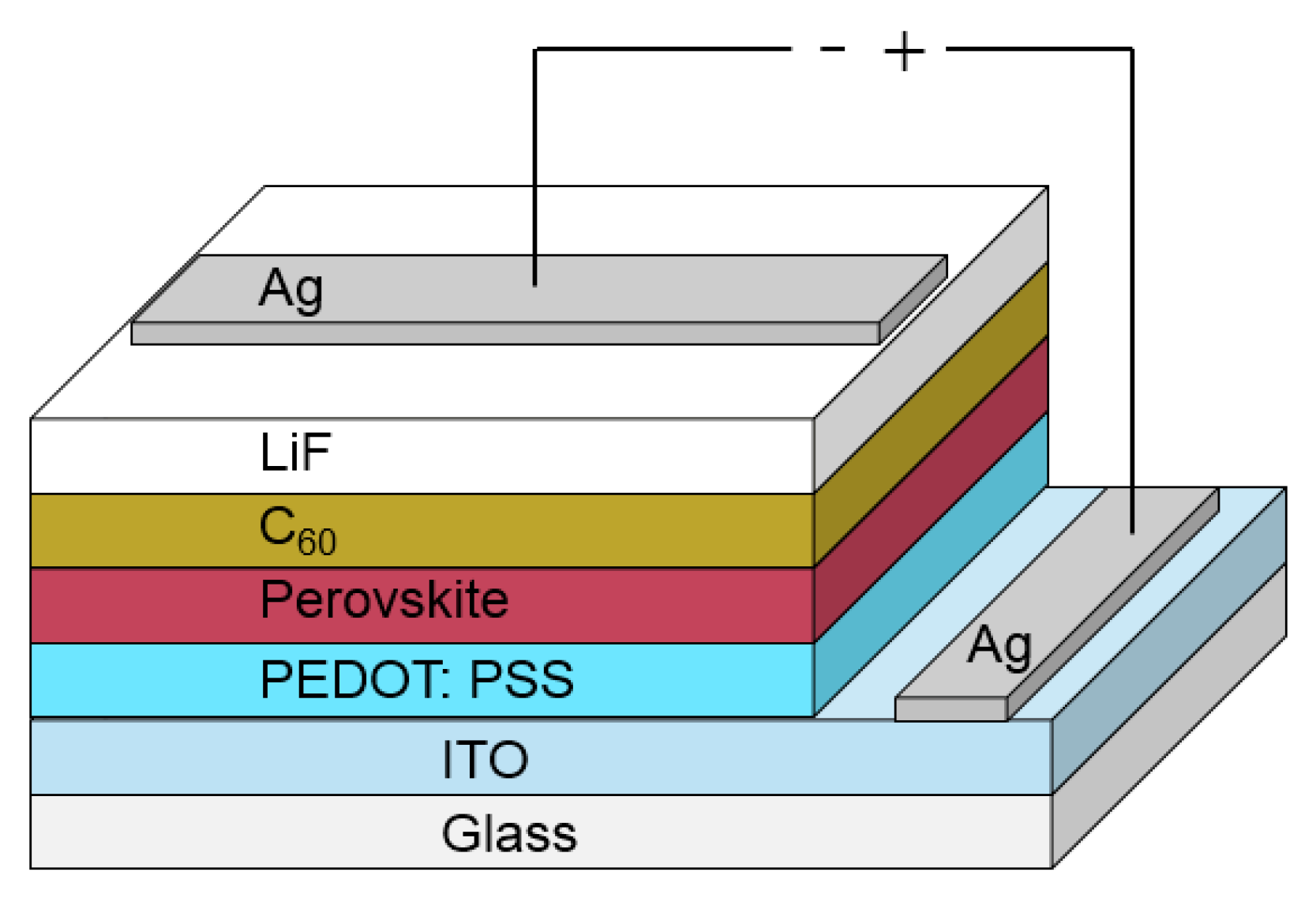
| Layer | Deposition Method | Thickness |
|---|---|---|
| Glass | - | 1.1 mm |
| ITO | - | around 150 nm |
| PEDOT:PSS | Spin-coated | 30 nm |
| Perovskite | Spin-coated | 300 nm |
| C60 | Evaporated | 20 nm |
| LiF | Evaporated | 1 nm |
| Ag | evaporated | 100 nm |
© 2016 by the authors. Licensee MDPI, Basel, Switzerland. This article is an open access article distributed under the terms and conditions of the Creative Commons by Attribution (CC-BY) license ( http://creativecommons.org/licenses/by/4.0/).
Share and Cite
Hu, H.; Wong, K.K.; Kollek, T.; Hanusch, F.; Polarz, S.; Docampo, P.; Schmidt-Mende, L. Highly Efficient Reproducible Perovskite Solar Cells Prepared by Low-Temperature Processing. Molecules 2016, 21, 542. https://doi.org/10.3390/molecules21040542
Hu H, Wong KK, Kollek T, Hanusch F, Polarz S, Docampo P, Schmidt-Mende L. Highly Efficient Reproducible Perovskite Solar Cells Prepared by Low-Temperature Processing. Molecules. 2016; 21(4):542. https://doi.org/10.3390/molecules21040542
Chicago/Turabian StyleHu, Hao, Ka Kan Wong, Tom Kollek, Fabian Hanusch, Sebastian Polarz, Pablo Docampo, and Lukas Schmidt-Mende. 2016. "Highly Efficient Reproducible Perovskite Solar Cells Prepared by Low-Temperature Processing" Molecules 21, no. 4: 542. https://doi.org/10.3390/molecules21040542
APA StyleHu, H., Wong, K. K., Kollek, T., Hanusch, F., Polarz, S., Docampo, P., & Schmidt-Mende, L. (2016). Highly Efficient Reproducible Perovskite Solar Cells Prepared by Low-Temperature Processing. Molecules, 21(4), 542. https://doi.org/10.3390/molecules21040542