
Recent Advances in Interface Engineering for Planar Heterojunction Perovskite Solar Cells

Abstract
:1. Introduction
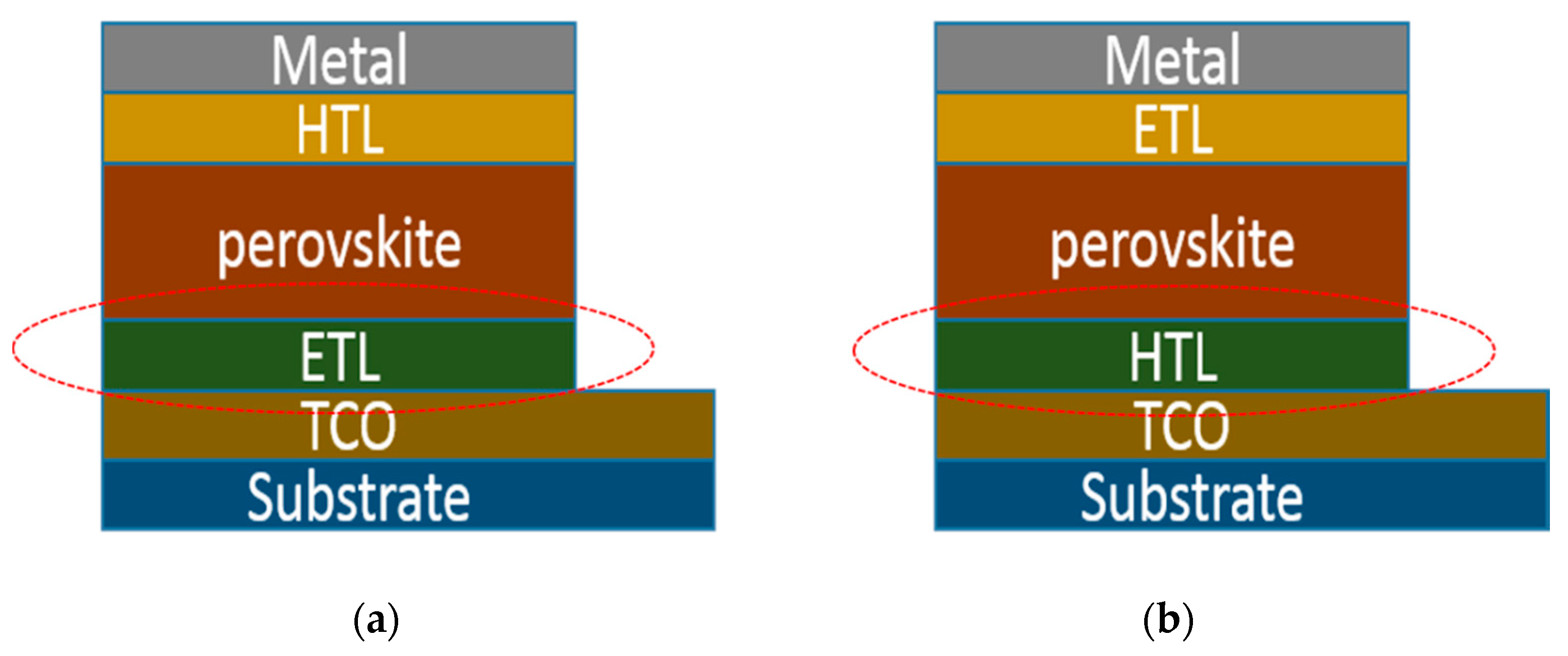
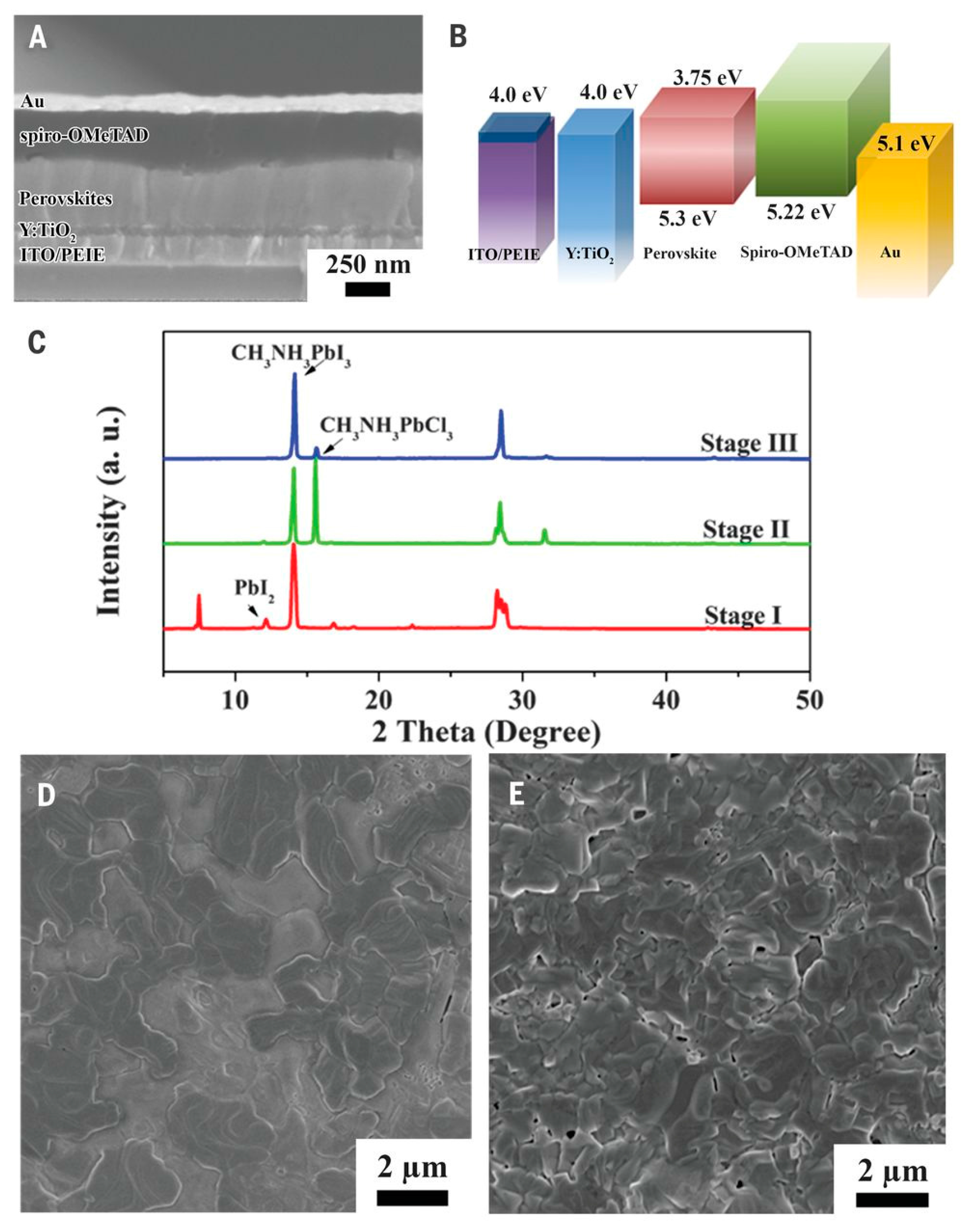
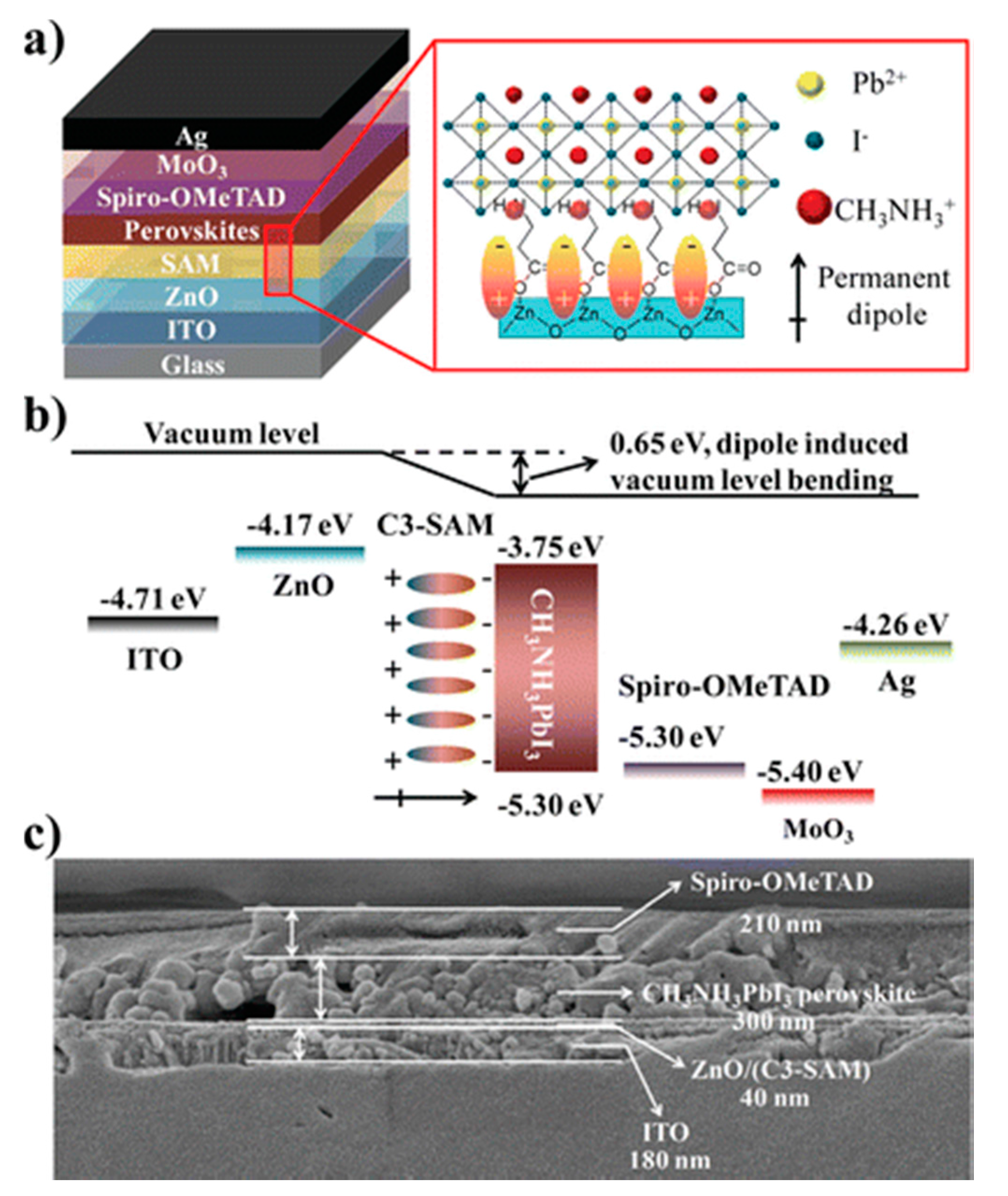
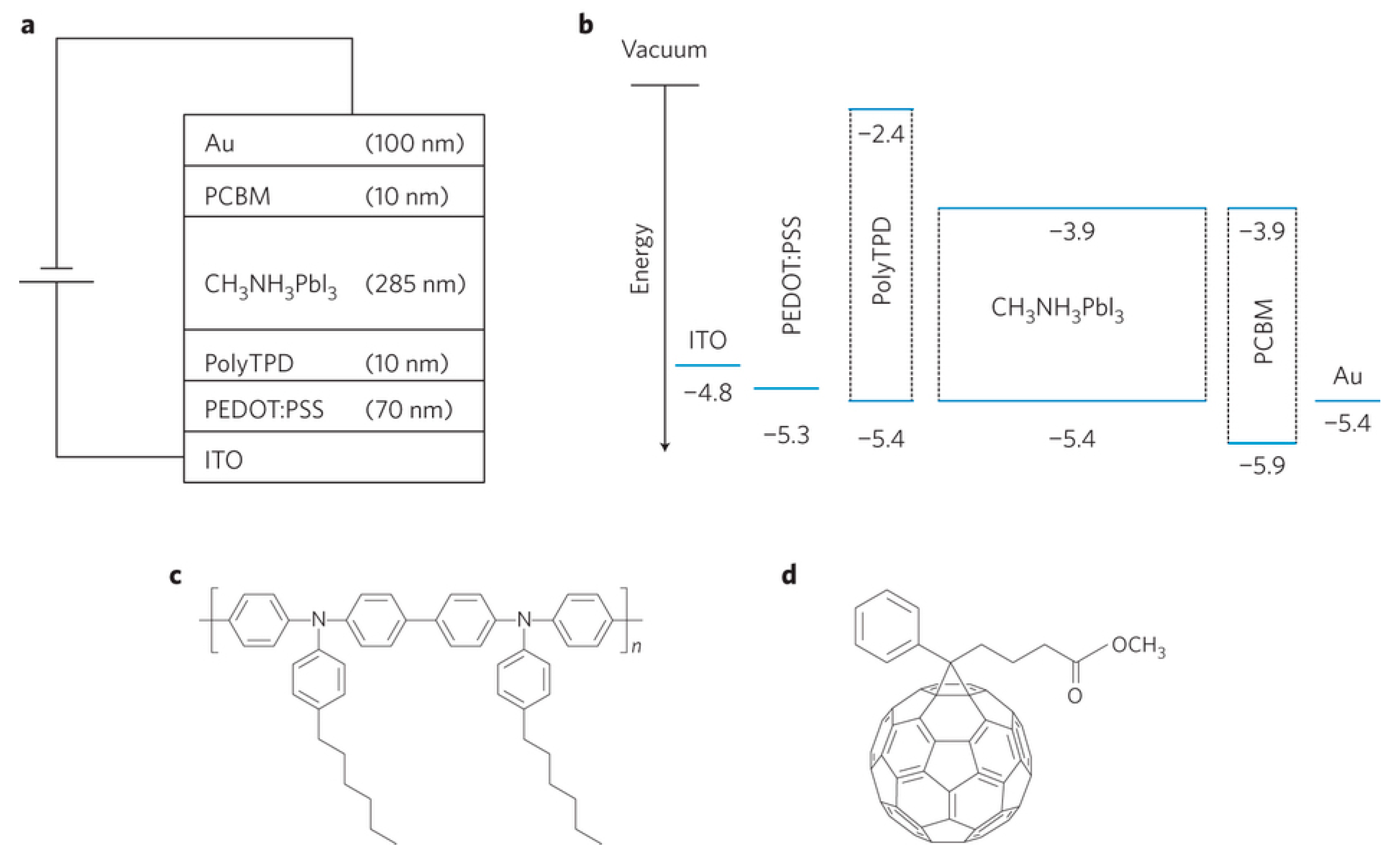
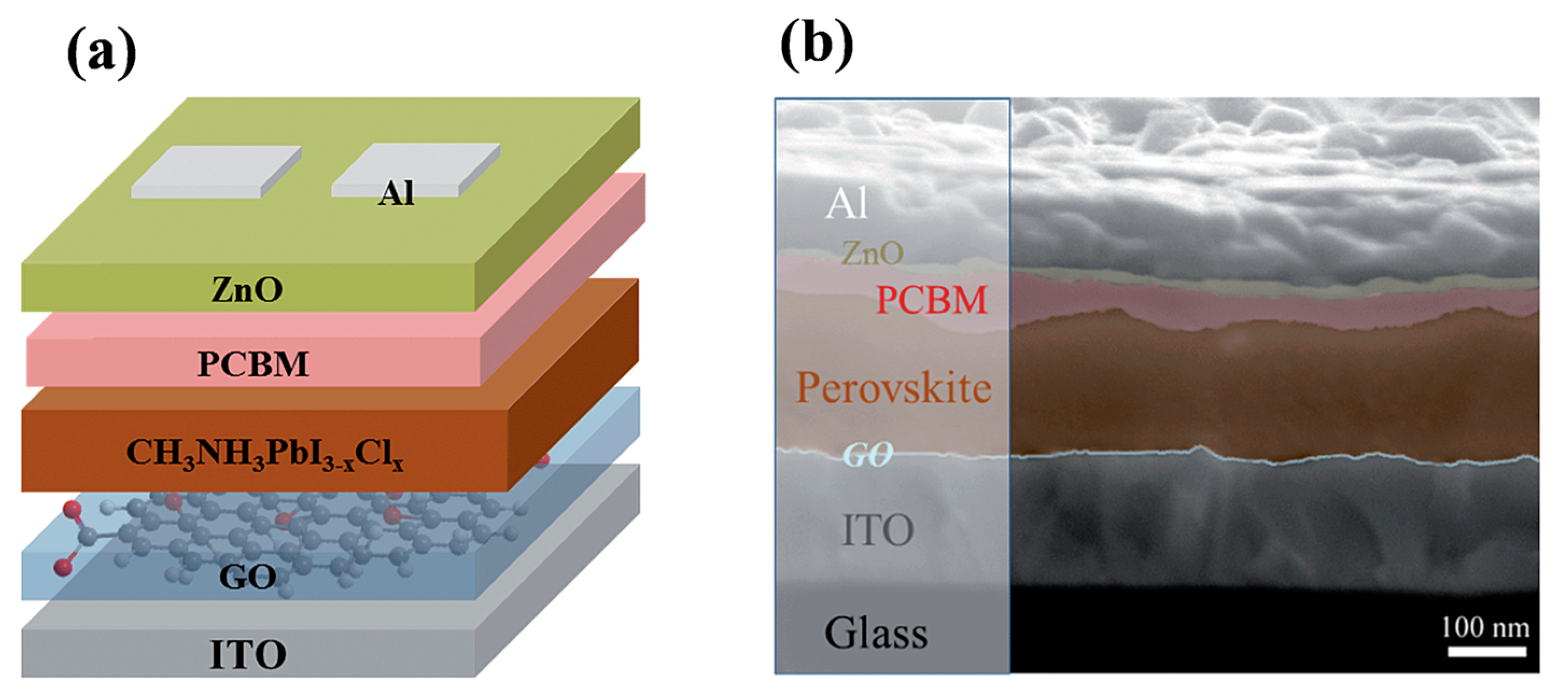
2. Metal Oxide
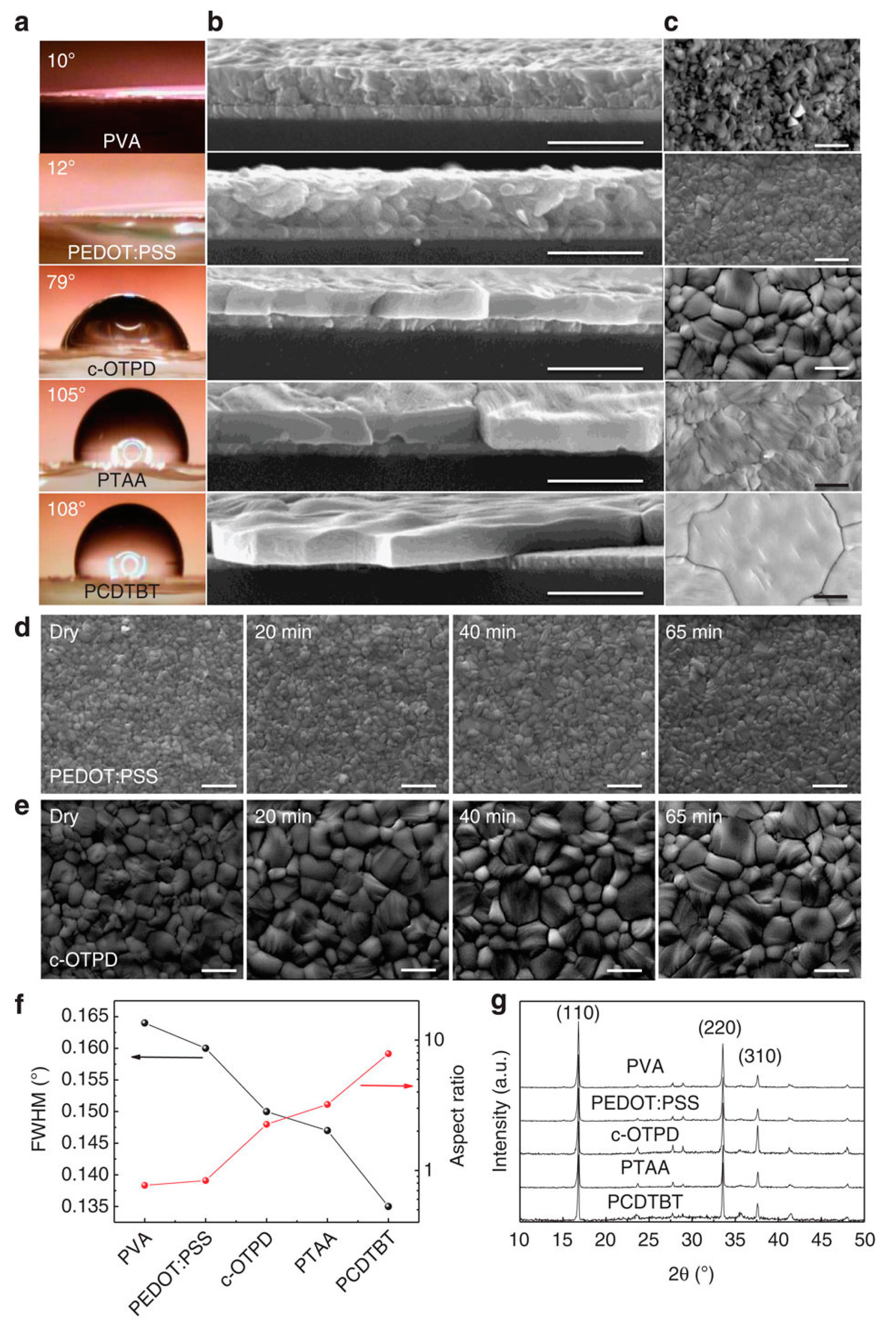
3. Molecular Interfacial Materials
4. Other Interface Materials
5. Summary and Outlook
Acknowledgments
Conflicts of Interest
References
- Burschka, J.; Pellet, N.; Moon, S.-J.; Humphry-Baker, R.; Gao, P.; Nazeeruddin, M.K.; Grätzel, M. Sequential deposition as a route to high-performance perovskite-sensitized solar cells. Nature 2013, 499, 316–319. [Google Scholar] [CrossRef] [PubMed]
- Jeon, N.J.; Noh, J.H.; Yang, W.S.; Kim, Y.C.; Ryu, S.; Seo, J.; Seok, S.I. Compositional engineering of perovskite materials for high-performance solar cells. Nature 2015, 517, 476–480. [Google Scholar] [CrossRef] [PubMed]
- Liu, M.; Johnston, M.B.; Snaith, H.J. Efficient planar heterojunction perovskite solar cells by vapour deposition. Nature 2013, 501, 395–398. [Google Scholar] [CrossRef] [PubMed]
- Park, N.-G. Perovskite solar cells: An emerging photovoltaic technology. Mater. Today 2015, 18, 65–72. [Google Scholar] [CrossRef]
- Boix, P.P.; Nonomura, K.; Mathews, N.; Mhaisalkar, S.G. Current progress and future perspectives for organic/inorganic perovskite solar cells. Mater. Today 2014, 17, 16–23. [Google Scholar] [CrossRef]
- Shi, S.; Li, Y.; Li, X.; Wang, H. Advancements in all-solid-state hybrid solar cells based on organometal halide perovskites. Mater. Horiz. 2015, 2, 378–405. [Google Scholar] [CrossRef]
- Lee, M.M.; Teuscher, J.; Miyasaka, T.; Murakami, T.N.; Snaith, H.J. Efficient hybrid solar cells based on meso-superstructured organometal halide perovskites. Science 2012, 338, 643–647. [Google Scholar] [CrossRef] [PubMed]
- Gao, P.; Grätzel, M.; Nazeeruddin, M.K. Organohalide lead perovskites for photovoltaic applications. Energy Environ. Sci. 2014, 7, 2448–2463. [Google Scholar] [CrossRef]
- Singh, S.P.; Nagarjuna, P. Organometal halide perovskites as useful materials in sensitized solar cells. Dalton Trans. 2014, 43, 5247–5251. [Google Scholar] [CrossRef] [PubMed]
- Grätzel, M. The light and shade of perovskite solar cells. Nat. Mater. 2014, 13, 838–842. [Google Scholar] [CrossRef] [PubMed]
- Kojima, A.; Teshima, K.; Shirai, Y.; Miyasaka, T. Organometal halide perovskites as visible-light sensitizers for photovoltaic cells. J. Am. Chem. Soc. 2009, 131, 6050–6051. [Google Scholar] [CrossRef] [PubMed]
- Zhou, H.; Chen, Q.; Li, G.; Luo, S.; Song, T.-B.; Duan, H.-S.; Hong, Z.; You, J.; Liu, Y.; Yang, Y. Interface engineering of highly efficient perovskite solar cells. Science 2014, 345, 542–546. [Google Scholar] [CrossRef] [PubMed]
- Yang, W.S.; Noh, J.H.; Jeon, N.J.; Kim, Y.C.; Ryu, S.; Seo, J.; Seok, S.I. High-performance photovoltaic perovskite layers fabricated through intramolecular exchange. Science 2015, 348, 1234–1237. [Google Scholar] [CrossRef] [PubMed]
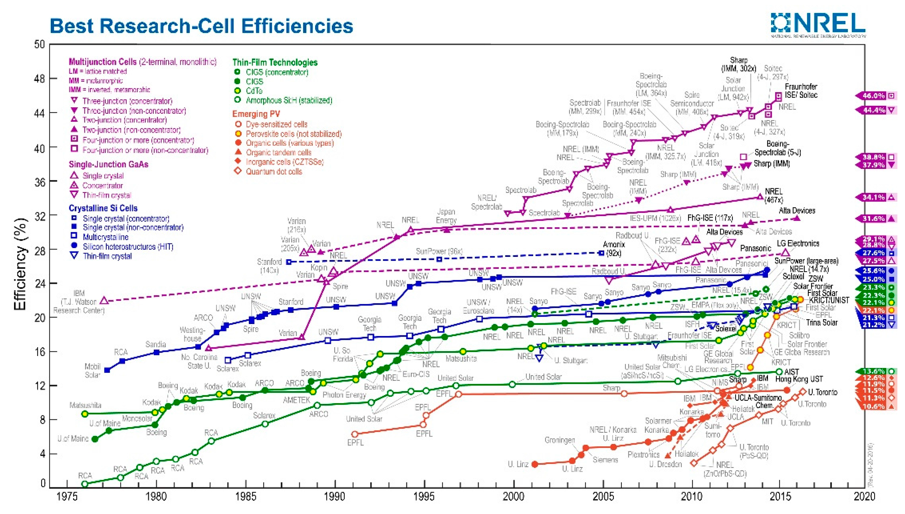
- N.R.E.L(NREL). Best Research-Cell Efficiencies. 2016. Availiable online: http://www.nrel.gov/ncpv/images/efficiency_chart.jpg. (accessed on 23 June 2016). [Google Scholar]
- Im, J.-H.; Lee, C.-R.; Lee, J.-W.; Park, S.-W.; Park, N.-G. 6.5% efficient perovskite quantum-dot-sensitized solar cell. Nanoscale 2011, 3, 4088–4093. [Google Scholar] [CrossRef] [PubMed]
- Kim, H.S.; Lee, C.R.; Im, J.H.; Lee, K.B.; Moehl, T.; Marchioro, A.; Moon, S.J.; Humphry-Baker, R.; Yum, J.H.; Moser, J.E.; et al. Lead iodide perovskite sensitized all-solid-state submicron thin film mesoscopic solar cell with efficiency exceeding 9%. Sci. Rep. 2012, 2, 591. [Google Scholar] [CrossRef] [PubMed]
- Etgar, L.; Gao, P.; Xue, Z.; Peng, Q.; Chandiran, A.K.; Liu, B.; Nazeeruddin, M.K.; Grä̈tzel, M. Mesoscopic CH3NH3PbI3/TiO2 heterojunction solar cells. J. Am. Chem. Soc. 2012, 134, 17396–17399. [Google Scholar] [CrossRef] [PubMed]
- Jeng, J.Y.; Chiang, Y.F.; Lee, M.H.; Peng, S.R.; Guo, T.F.; Chen, P.; Wen, T.C. CH3NH3PbI3 perovskite/fullerene planar-heterojunction hybrid solar cells. Adv. Mater. 2013, 25, 3727–3732. [Google Scholar] [CrossRef] [PubMed]
- Liang, P.W.; Liao, C.Y.; Chueh, C.C.; Zuo, F.; Williams, S.T.; Xin, X.K.; Lin, J.; Jen, A.K.Y. Additive enhanced crystallization of solution-processed perovskite for highly efficient planar-heterojunction solar cells. Adv. Mater. 2014, 26, 3748–3754. [Google Scholar] [CrossRef] [PubMed]
- Xiao, Z.; Bi, C.; Shao, Y.; Dong, Q.; Wang, Q.; Yuan, Y.; Wang, C.; Gao, Y.; Huang, J. Efficient, high yield perovskite photovoltaic devices grown by interdiffusion of solution-processed precursor stacking layers. Energy Environ. Sci. 2014, 7, 2619–2623. [Google Scholar] [CrossRef]
- Xie, F.X.; Zhang, D.; Su, H.; Ren, X.; Wong, K.S.; Grätzel, M.; Choy, W.C. Vacuum-assisted thermal annealing of CH3NH3PbI3 for highly stable and efficient perovskite solar cells. ACS Nano 2015, 9, 639–646. [Google Scholar] [CrossRef] [PubMed]
- Nie, W.; Tsai, H.; Asadpour, R.; Blancon, J.-C.; Neukirch, A.J.; Gupta, G.; Crochet, J.J.; Chhowalla, M.; Tretiak, S.; Alam, M.A. High-efficiency solution-processed perovskite solar cells with millimeter-scale grains. Science 2015, 347, 522–525. [Google Scholar] [CrossRef] [PubMed]
- Bi, C.; Wang, Q.; Shao, Y.; Yuan, Y.; Xiao, Z.; Huang, J. Non-wetting surface-driven high-aspect-ratio crystalline grain growth for efficient hybrid perovskite solar cells. Nat. Commun. 2015, 6, 7747. [Google Scholar] [CrossRef] [PubMed]
- Chiang, T.-Y.; Fan, G.-L.; Jeng, J.-Y.; Chen, K.-C.; Chen, P.; Wen, T.-C.; Guo, T.-F.; Wong, K.-T. Functional p-type, polymerized organic electrode interlayer in CH3NH3PbI3 perovskite/fullerene planar heterojunction hybrid solar cells. ACS Appl. Mater. Interfaces 2015, 7, 24973–24981. [Google Scholar] [CrossRef] [PubMed]
- Kim, H.; Lim, K.-G.; Lee, T.-W. Planar heterojunction organometal halide perovskite solar cells: Roles of interfacial layers. Energy Environ. Sci. 2016, 9, 12–30. [Google Scholar] [CrossRef]
- Fu-Zhi, W.; Zhan-Ao, T.; Song-Yuan, D.; Yong-Fang, L. Recent advances in planar heterojunction organic-inorganic hybrid perovskite solar cells. Acta Phys. Sin. 2015, 64. [Google Scholar] [CrossRef]
- Wang, K.C.; Jeng, J.Y.; Shen, P.S.; Chang, Y.C.; Diau, E.W.; Tsai, C.H.; Chao, T.Y.; Hsu, H.C.; Lin, P.Y.; Chen, P.; et al. P-type mesoscopic nickel oxide/organometallic perovskite heterojunction solar cells. Sci. Rep. 2014, 4, 4756. [Google Scholar] [CrossRef] [PubMed]
- Kim, J.H.; Liang, P.W.; Williams, S.T.; Cho, N.; Chueh, C.C.; Glaz, M.S.; Ginger, D.S.; Jen, A.K.Y. High-performance and environmentally stable planar heterojunction perovskite solar cells based on a solution-processed copper-doped nickel oxide hole-transporting layer. Adv. Mater. 2015, 27, 695–701. [Google Scholar] [CrossRef] [PubMed]
- Park, J.H.; Seo, J.; Park, S.; Shin, S.S.; Kim, Y.C.; Jeon, N.J.; Shin, H.W.; Ahn, T.K.; Noh, J.H.; Yoon, S.C. Efficient CH3NH3PbI3 perovskite solar cells employing nanostructured p-type NiO electrode formed by a pulsed laser deposition. Adv. Mater. 2015, 27, 4013–4019. [Google Scholar] [CrossRef] [PubMed]
- Malinkiewicz, O.; Yella, A.; Lee, Y.H.; Espallargas, G.M.; Graetzel, M.; Nazeeruddin, M.K.; Bolink, H.J. Perovskite solar cells employing organic charge-transport layers. Nat. Photonics 2014, 8, 128–132. [Google Scholar] [CrossRef]
- Yang, G.; Tao, H.; Qin, P.; Ke, W.; Fang, G. Recent progress in electron transport layers for efficient perovskite solar cells. J. Mater. Chem. A 2016, 4, 3970–3990. [Google Scholar] [CrossRef]
- Mali, S.S.; Hong, C.K. Pin/nip type planar hybrid structure of highly efficient perovskite solar cells towards improved air stability: Synthetic strategies and the role of p-type hole transport layer (HTL) and n-type electron transport layer (ETL) metal oxides. Nanoscale 2016, 8, 10528–10540. [Google Scholar] [CrossRef] [PubMed]
- Chen, L.; Wang, J.-R.; Xie, L.-Q.; Zhan, C.; Qiu, Z.; Zhou, J.-Z.; Yan, J.-W.; Mao, B.-W.; Tian, Z.-Q. Compact layer influence on hysteresis effect in organic–inorganic hybrid perovskite solar cells. Electrochem. Commun. 2016, 68, 40–44. [Google Scholar] [CrossRef]
- Yan, W.; Ye, S.; Li, Y.; Sun, W.; Rao, H.; Liu, Z.; Bian, Z.; Huang, C. Hole-transporting materials in inverted planar perovskite solar cells. Adv. Energy Mater. 2016. [Google Scholar] [CrossRef]
- Gheno, A.; Vedraine, S.; Ratier, B.; Bouclé, J. Π-conjugated materials as the hole-transporting layer in perovskite solar cells. Metals 2016, 6, 21. [Google Scholar] [CrossRef]
- Wojciechowski, K.; Saliba, M.; Leijtens, T.; Abate, A.; Snaith, H.J. Sub-150 c processed meso-superstructured perovskite solar cells with enhanced efficiency. Energy Environ. Sci. 2014, 7, 1142–1147. [Google Scholar] [CrossRef]
- Zhu, Q.; Bao, X.; Yu, J.; Zhu, D.; Qiu, M.; Yang, R.; Dong, L. Compact layer free perovskite solar cells with a high-mobility hole-transporting layer. ACS Appl. Mater. Interfaces 2016, 8, 2652–2657. [Google Scholar] [CrossRef] [PubMed]
- Yella, A.; Heiniger, L.-P.; Gao, P.; Nazeeruddin, M.K.; Grätzel, M. Nanocrystalline rutile electron extraction layer enables low-temperature solution processed perovskite photovoltaics with 13.7% efficiency. Nano Lett. 2014, 14, 2591–2596. [Google Scholar]
- Liu, Z.; Chen, Q.; Hong, Z.; Zhou, H.; Xu, X.; de Marco, N.; Sun, P.; Zhao, Z.; Cheng, Y.-B.; Yang, Y. Low-temperature tio x compact layer for planar heterojunction perovskite solar cells. ACS Appl. Mater. Interfaces 2016, 8, 11076–11083. [Google Scholar] [CrossRef] [PubMed]
- Choi, J.M.; Song, S.; Hörantner, M.T.; Snaith, H.J.; Park, T. A well-defined nanostructured, single crystalline TiO2 electron transport layer for efficient planar perovskite solar cells. ACS Nano 2016. [Google Scholar] [CrossRef] [PubMed]
- Lv, M.; Lv, W.; Fang, X.; Sun, P.; Lin, B.; Zhang, S.; Xu, X.; Ding, J.; Yuan, N. Performance enhancement of perovskite solar cells with a modified TiO2 electron transport layer using Zn-based additives. RSC Adv. 2016, 6, 35044–35050. [Google Scholar] [CrossRef]
- Meng, T.; Liu, C.; Wang, K.; He, T.; Zhu, Y.; Al-Enizi, A.M.; Elzatahry, A.A.; Gong, X. High performance perovskite hybrid solar cells with e-beam-processed tiox electron extraction layer. ACS Appl. Mater. Interfaces 2016, 8, 1876–1883. [Google Scholar] [CrossRef] [PubMed]
- Huang, C.; Liu, C.; Di, Y.; Li, W.; Liu, F.; Jiang, L.; Li, J.; Hao, X.; Huang, H. Efficient planar perovskite solar cells with reduced hysteresis and enhanced open circuit voltage by using PW12–TiO2 as electron transport layer. ACS Appl. Mater. Interfaces 2016, 8, 8520–8526. [Google Scholar] [CrossRef] [PubMed]
- Du, Y.Y.; Cai, H.; Wen, H.; Wu, Y.; Huang, L.; Ni, J.; Li, J.; Zhang, J. Novel combination of efficient perovskite solar cells with low temperature processed compact TiO2 layer via anodic oxidation. ACS Appl. Mater. Interfaces 2016, 8, 12836–12842. [Google Scholar] [CrossRef] [PubMed]
- Ke, W.; Fang, G.; Wan, J.; Tao, H.; Liu, Q.; Xiong, L.; Qin, P.; Wang, J.; Lei, H.; Yang, G.; et al. Efficient hole-blocking layer-free planar halide perovskite thin-film solar cells. Nat. Commun. 2015, 6, 7700. [Google Scholar] [CrossRef] [PubMed]
- Zhang, Q.; Dandeneau, C.S.; Zhou, X.; Cao, G. ZnO nanostructures for dye-sensitized solar cells. Adv. Mater. 2009, 21, 4087–4108. [Google Scholar] [CrossRef]
- Liu, D.; Kelly, T.L. Perovskite solar cells with a planar heterojunction structure prepared using room-temperature solution processing techniques. Nat. Photonics 2014, 8, 133–138. [Google Scholar] [CrossRef]
- Zuo, L.; Gu, Z.; Ye, T.; Fu, W.; Wu, G.; Li, H.; Chen, H. Enhanced photovoltaic performance of CH3NH3PbI3 perovskite solar cells through interfacial engineering using self-assembling monolayer. J. Am. Chem. Soc. 2015, 137, 2674–2679. [Google Scholar] [CrossRef] [PubMed]
- Cheng, M.; Xu, B.; Chen, C.; Yang, X.; Zhang, F.; Tan, Q.; Hua, Y.; Kloo, L.; Sun, L. Phenoxazine-based small molecule material for efficient perovskite solar cells and bulk heterojunction organic solar cells. Adv. Energy Mater. 2015, 5. [Google Scholar] [CrossRef]
- Qin, M.; Ma, J.; Ke, W.; Qin, P.; Lei, H.; Tao, H.; Zheng, X.; Xiong, L.; Liu, Q.; Chen, Z. Perovskite solar cells based on low-temperature processed indium oxide electron selective layers. ACS Appl. Mater. Interfaces 2016, 8, 8460–8466. [Google Scholar] [CrossRef] [PubMed]
- Guerrero, A.; Garcia-Belmonte, G.; Mora-Sero, I.; Bisquert, J.; Kang, Y.S.; Jacobsson, T.J.; Correa-Baena, J.-P.; Hagfeldt, A. Properties of contact and bulk impedances in hybrid lead halide perovskite solar cells including inductive loop elements. J. Phys. Chem. C 2016, 120, 8023–8032. [Google Scholar] [CrossRef]
- Irwin, M.D.; Buchholz, D.B.; Hains, A.W.; Chang, R.P.; Marks, T.J. P-type semiconducting nickel oxide as an efficiency-enhancing anode interfacial layer in polymer bulk-heterojunction solar cells. Proc. Natl. Acad. Sci. USA 2008, 105, 2783–2787. [Google Scholar] [CrossRef]
- Steirer, K.X.; Ndione, P.F.; Widjonarko, N.E.; Lloyd, M.T.; Meyer, J.; Ratcliff, E.L.; Kahn, A.; Armstrong, N.R.; Curtis, C.J.; Ginley, D.S. Enhanced efficiency in plastic solar cells via energy matched solution processed NiOx interlayers. Adv. Energy Mater. 2011, 1, 813–820. [Google Scholar] [CrossRef]
- Jeng, J.Y.; Chen, K.C.; Chiang, T.Y.; Lin, P.Y.; Tsai, T.D.; Chang, Y.C.; Guo, T.F.; Chen, P.; Wen, T.C.; Hsu, Y.J. Nickel oxide electrode interlayer in CH3NH3PbI3 perovskite/pcbm planar-heterojunction hybrid solar cells. Adv. Mater. 2014, 26, 4107–4113. [Google Scholar] [CrossRef] [PubMed]
- Edri, E.; Kirmayer, S.; Kulbak, M.; Hodes, G.; Cahen, D. Chloride inclusion and hole transport material doping to improve methyl ammonium lead bromide perovskite-based high open-circuit voltage solar cells. J. Phys. Chem. Lett. 2014, 5, 429–433. [Google Scholar] [CrossRef] [PubMed]
- Jung, J.W.; Chueh, C.C.; Jen, A.K.Y. A low-temperature, solution-processable, Cu-doped nickel oxide hole-transporting layer via the combustion method for high-performance thin-film perovskite solar cells. Adv. Mater. 2015, 27, 7874–7880. [Google Scholar] [CrossRef] [PubMed]
- Hou, Y.; Chen, W.; Baran, D.; Stubhan, T.; Luechinger, N.A.; Hartmeier, B.; Richter, M.; Min, J.; Chen, S.; Quiroz, C.O.R. Overcoming the interface losses in planar heterojunction perovskite-based solar cells. Adv. Mater. 2016. [Google Scholar] [CrossRef] [PubMed]
- Yin, X.; Chen, P.; Que, M.; Xing, Y.; Que, W.; Niu, C.; Shao, J. Highly efficient flexible perovskite solar cells using solution-derived NiOx hole contacts. ACS Nano 2016, 10, 3630–3636. [Google Scholar] [CrossRef] [PubMed]
- You, J.; Meng, L.; Song, T.-B.; Guo, T.-F.; Yang, Y.M.; Chang, W.-H.; Hong, Z.; Chen, H.; Zhou, H.; Chen, Q. Improved air stability of perovskite solar cells via solution-processed metal oxide transport layers. Nat. Nanotechnol. 2016, 11, 75–81. [Google Scholar] [CrossRef] [PubMed]
- Choi, H.; Mai, C.-K.; Kim, H.-B.; Jeong, J.; Song, S.; Bazan, G.C.; Kim, J.Y.; Heeger, A.J. Conjugated polyelectrolyte hole transport layer for inverted-type perovskite solar cells. Nat. Commun. 2015, 6. [Google Scholar] [CrossRef] [PubMed]
- Feng, S.; Yang, Y.; Li, M.; Wang, J.; Cheng, Z.; Li, J.; Ji, G.; Yin, G.; Song, F.; Wang, Z.-K. High-performance perovskite solar cells engineered by an ammonia modified graphene oxide interfacial layer. ACS Appl. Mater. Interfaces 2016, 8, 14503–14512. [Google Scholar] [CrossRef] [PubMed]
- Spiccia, L.; Xiao, M.; Gao, M.; Pascoe, A.; Qin, T.; Huang, F.; Bach, U.; Cheng, Y.-B. Efficient perovskite solar cells employing inorganic interlayers. ChemNanoMat 2016, 2, 182–188. [Google Scholar]
- Sun, H.; Hou, X.; Wei, Q.; Liu, H.; Yang, K.; Wang, W.; An, Q.; Rong, Y. Low-temperature solution-processed p-type vanadium oxide for perovskite solar cells. Chem. Commun. 2016, 52, 8099–8102. [Google Scholar] [CrossRef] [PubMed]
- Xia, Y.; Zhang, H.; Ouyang, J. Highly conductive pedot: Pss films prepared through a treatment with zwitterions and their application in polymer photovoltaic cells. J. Mater. Chem. 2010, 20, 9740–9747. [Google Scholar] [CrossRef]
- Li, G.; Chu, C.; Shrotriya, V.; Huang, J.; Yang, Y. Efficient inverted polymer solar cells. Appl. Phys. Lett. 2006, 88, 253503–253503. [Google Scholar] [CrossRef]
- Kim, Y.; Ballantyne, A.M.; Nelson, J.; Bradley, D.D. Effects of thickness and thermal annealing of the pedot: Pss layer on the performance of polymer solar cells. Org. Electron. 2009, 10, 205–209. [Google Scholar] [CrossRef]
- Zhang, Y.; Hu, X.; Chen, L.; Huang, Z.; Fu, Q.; Liu, Y.; Zhang, L.; Chen, Y. Flexible, hole transporting layer-free and stable CH3NH3PbI3/PC61BM planar heterojunction perovskite solar cells. Org. Electron. 2016, 30, 281–288. [Google Scholar] [CrossRef]
- Li, D.; Cui, J.; Zhang, H.; Li, H.; Wang, M.; Shen, Y. Effect of hole transport layer in planar inverted perovskite solar cells. Chem. Lett. 2016. [Google Scholar] [CrossRef]
- Wu, Y.; Wang, J.; Qiu, X.; Yang, R.; Lou, H.; Bao, X.; Li, Y. Highly efficient inverted perovskite solar cells with sulfonated lignin doped pedot as hole extract layer. ACS Appl. Mater. Interfaces 2016, 8, 12377–12383. [Google Scholar] [CrossRef] [PubMed]
- Li, C. Poly (3, 4-ethylenedioxythiophene): Poly (styrenesulfonate)(pedot: Pss)-molybdenum oxide composite films as hole conductor for efficient planar perovskite solar cells. J. Mater. Chem. A 2016, 4, 9958–9966. [Google Scholar]
- Liu, C.; Su, Z.; Li, W.; Jin, F.; Chu, B.; Wang, J.; Zhao, H.; Lee, C.; Tang, J.; Kang, B. Improved performance of perovskite solar cells with a TiO2/MoO3 core/shell nanoparticles doped pedot: Pss hole-transporter. Org. Electron. 2016, 33, 221–226. [Google Scholar] [CrossRef]
- Qian, M.; Li, M.; Shi, X.-B.; Ma, H.; Wang, Z.-K.; Liao, L.-S. Planar perovskite solar cells with 15.75% power conversion efficiency by cathode and anode interfacial modification. J. Mater. Chem. A 2015, 3, 13533–13539. [Google Scholar] [CrossRef]
- Lim, K.G.; Kim, H.B.; Jeong, J.; Kim, H.; Kim, J.Y.; Lee, T.W. Boosting the power conversion efficiency of perovskite solar cells using self-organized polymeric hole extraction layers with high work function. Adv. Mater. 2014, 26, 6461–6466. [Google Scholar] [CrossRef] [PubMed]
- Yoon, H.; Kang, S.M.; Lee, J.-K.; Choi, M. Hysteresis-free low-temperature-processed planar perovskite solar cells with 19.1% efficiency. Energy Environ. Sci. 2016. [Google Scholar] [CrossRef]
- Ball, J.M.; Lee, M.M.; Hey, A.; Snaith, H.J. Low-temperature processed meso-superstructured to thin-film perovskite solar cells. Energy Environ. Sci. 2013, 6, 1739–1743. [Google Scholar] [CrossRef]
- Zhou, H.; Zhang, Y.; Mai, C.K.; Collins, S.D.; Nguyen, T.Q.; Bazan, G.C.; Heeger, A.J. Conductive conjugated polyelectrolyte as hole-transporting layer for organic bulk heterojunction solar cells. Adv. Mater. 2014, 26, 780–785. [Google Scholar] [CrossRef] [PubMed]
- Shao, Y.; Xiao, Z.; Bi, C.; Yuan, Y.; Huang, J. Origin and elimination of photocurrent hysteresis by fullerene passivation in CH3NH3PbI3 planar heterojunction solar cells. Nat. Commun. 2014, 5, 5784. [Google Scholar] [CrossRef] [PubMed]
- Chen, Q.; Zhou, H.; Hong, Z.; Luo, S.; Duan, H.-S.; Wang, H.-H.; Liu, Y.; Li, G.; Yang, Y. Planar heterojunction perovskite solar cells via vapor-assisted solution process. J. Am. Chem. Soc. 2013, 136, 622–625. [Google Scholar] [CrossRef] [PubMed]
- Dong, Q.; Fang, Y.; Shao, Y.; Mulligan, P.; Qiu, J.; Cao, L.; Huang, J. Electron-hole diffusion lengths> 175 μm in solution-grown CH3NH3PbI3 single crystals. Science 2015, 347, 967–970. [Google Scholar] [CrossRef] [PubMed]
- Wang, L.; McCleese, C.; Kovalsky, A.; Zhao, Y.; Burda, C. Femtosecond time-resolved transient absorption spectroscopy of CH3NH3PbI3 perovskite films: Evidence for passivation effect of PbI2. J. Am. Chem. Soc. 2014, 136, 12205–12208. [Google Scholar] [CrossRef] [PubMed]
- Abrusci, A.; Stranks, S.D.; Docampo, P.; Yip, H.-L.; Jen, A.K.-Y.; Snaith, H.J. High-performance perovskite-polymer hybrid solar cells via electronic coupling with fullerene monolayers. Nano Lett. 2013, 13, 3124–3128. [Google Scholar] [CrossRef] [PubMed]
- Wu, Z.; Bai, S.; Xiang, J.; Yuan, Z.; Yang, Y.; Cui, W.; Gao, X.; Liu, Z.; Jin, Y.; Sun, B. Efficient planar heterojunction perovskite solar cells employing graphene oxide as hole conductor. Nanoscale 2014, 6, 10505–10510. [Google Scholar] [CrossRef] [PubMed]
- Chen, W.; Wu, Y.; Yue, Y.; Liu, J.; Zhang, W.; Yang, X.; Chen, H.; Bi, E.; Ashraful, I.; Grätzel, M. Efficient and stable large-area perovskite solar cells with inorganic charge extraction layers. Science 2015, 350, 944–948. [Google Scholar] [CrossRef] [PubMed]
- Liu, J.; Xue, Y.; Dai, L. Sulfated graphene oxide as a hole-extraction layer in high-performance polymer solar cells. J. Phys. Chem. Lett. 2012, 3, 1928–1933. [Google Scholar] [CrossRef] [PubMed]
- Li, S.-S.; Tu, K.-H.; Lin, C.-C.; Chen, C.-W.; Chhowalla, M. Solution-processable graphene oxide as an efficient hole transport layer in polymer solar cells. ACS Nano 2010, 4, 3169–3174. [Google Scholar] [CrossRef] [PubMed]
- Gao, Y.; Yip, H.L.; Chen, K.S.; O’Malley, K.M.; Acton, O.; Sun, Y.; Ting, G.; Chen, H.; Jen, A.K.Y. Surface doping of conjugated polymers by graphene oxide and its application for organic electronic devices. Adv. Mater. 2011, 23, 1903–1908. [Google Scholar] [CrossRef] [PubMed]
- Li, D.; Cui, J.; Li, H.; Huang, D.; Wang, M.; Shen, Y. Graphene oxide modified hole transport layer for CH3NH3PbI planar heterojunction solar cells. Sol. Energy 2016, 131, 176–182. [Google Scholar] [CrossRef]
- Malinkiewicz, O.; Roldán-Carmona, C.; Soriano, A.; Bandiello, E.; Camacho, L.; Nazeeruddin, M.K.; Bolink, H.J. Metal-oxide-free methylammonium lead iodide perovskite-based solar cells: The influence of organic charge transport layers. Adv. Energy Mater. 2014, 4. [Google Scholar] [CrossRef]
- Yang, Z.; Cai, B.; Zhou, B.; Yao, T.; Yu, W.; Liu, S.F.; Zhang, W.-H.; Li, C. An up-scalable approach to CH3NH3PbI3 compact films for high-performance perovskite solar cells. Nano Energy 2015, 15, 670–678. [Google Scholar] [CrossRef]
- Hwang, I.; Yong, K. Novel CdS hole-blocking layer for photostable perovskite solar cells. ACS Appl. Mater. Interfaces 2016, 8, 4226–4232. [Google Scholar] [CrossRef] [PubMed]
- Rao, H.; Sun, W.; Ye, S.; Yan, W.; Li, Y.; Peng, H.; Liu, Z.; Bian, Z.; Huang, C. Solution-processed CuS NPs as an inorganic hole-selective contact material for inverted planar perovskite solar cells. ACS Appl. Mater. Interfaces 2016, 8, 7800–7805. [Google Scholar] [CrossRef] [PubMed]
- Zuo, C.; Ding, L. An 80.11% ff record achieved for perovskite solar cells by using the NH4Cl additive. Nanoscale 2014, 6, 9935–9938. [Google Scholar] [CrossRef] [PubMed]
- Eperon, G.E.; Stranks, S.D.; Menelaou, C.; Johnston, M.B.; Herz, L.M.; Snaith, H.J. Formamidinium lead trihalide: A broadly tunable perovskite for efficient planar heterojunction solar cells. Energy Environ. Sci. 2014, 7, 982–988. [Google Scholar] [CrossRef]
- Kim, H.-B.; Choi, H.; Jeong, J.; Kim, S.; Walker, B.; Song, S.; Kim, J.Y. Mixed solvents for the optimization of morphology in solution-processed, inverted-type perovskite/fullerene hybrid solar cells. Nanoscale 2014, 6, 6679–6683. [Google Scholar] [CrossRef] [PubMed]
- Jeon, N.J.; Noh, J.H.; Kim, Y.C.; Yang, W.S.; Ryu, S.; Seok, S.I. Solvent engineering for high-performance inorganic–organic hybrid perovskite solar cells. Nat. Mater. 2014, 13, 897–903. [Google Scholar] [CrossRef] [PubMed]
- Yan, K.; Long, M.; Zhang, T.; Wei, Z.; Chen, H.; Yang, S.; Xu, J. Hybrid halide perovskite solar cell precursors: Colloidal chemistry and coordination engineering behind device processing for high efficiency. J. Am. Chem. Soc. 2015, 137, 4460–4468. [Google Scholar] [CrossRef] [PubMed]
- Zhang, W.; Saliba, M.; Moore, D.T.; Pathak, S.K.; Hörantner, M.T.; Stergiopoulos, T.; Stranks, S.D.; Eperon, G.E.; Alexander-Webber, J.A.; Abate, A. Ultrasmooth organic–inorganic perovskite thin-film formation and crystallization for efficient planar heterojunction solar cells. Nat. Commun. 2015, 6. [Google Scholar] [CrossRef] [PubMed]
- Noel, N.K.; Stranks, S.D.; Abate, A.; Wehrenfennig, C.; Guarnera, S.; Haghighirad, A.-A.; Sadhanala, A.; Eperon, G.E.; Pathak, S.K.; Johnston, M.B. Lead-free organic–inorganic tin halide perovskites for photovoltaic applications. Energy Environ. Sci. 2014, 7, 3061–3068. [Google Scholar] [CrossRef]
- Hao, F.; Stoumpos, C.C.; Cao, D.H.; Chang, R.P.; Kanatzidis, M.G. Lead-free solid-state organic-inorganic halide perovskite solar cells. Nat. Photonics 2014, 8, 489–494. [Google Scholar] [CrossRef]
- Kumar, M.H.; Dharani, S.; Leong, W.L.; Boix, P.P.; Prabhakar, R.R.; Baikie, T.; Shi, C.; Ding, H.; Ramesh, R.; Asta, M. Lead-free halide perovskite solar cells with high photocurrents realized through vacancy modulation. Adv. Mater. 2014, 26, 7122–7127. [Google Scholar] [CrossRef] [PubMed]


| Device Structure | Voc (V) | Jsc (mAcm−2) | FF | PCE (%) | Ref. |
|---|---|---|---|---|---|
| ITO/TiCl-TiO2/CH3NH3PbI3−xClx/Spiro-OMeTAD/Au | 1.09 | 19.7 | 0.759 | 16.4 | [39] |
| FTO/A-TiO2/CH3NH3PbI3/Spiro-OMeTAD/Ag | 1.06 | 20.5 | 0.7 | 15.2 | [40] |
| FTO/Zn-TiO2/CH3NH3PbI3/Spiro-OMeTAD/Ag | 1.04 | 23.83 | 0.649 | 16.07 | [41] |
| ITO/AO-TiO2/CH3NH3PbI3−xClx/Spiro-OMeTAD/Au | 1.00 | 19.08 | 0.71 | 13.47 | [44] |
| FTO/PW12-TiO2/CH3NH3PbI3−xClx/Spiro-OMeTAD/Au | 1.1 | 20 | 0.7 | 15.45 | [43] |
| ITO/E-TiOX/CH3NH3PbI3/P3HT/MoO3/Ag | 0.93 | 27.8 | 0.57 | 14.7 | [42] |
| FTO/Zn-TiO2/CH3NH3PbI3/Spiro-OMeTAD/Au | 1.05 | 19.8 | 0.64 | 13.7 | [38] |
| ITO/PEIE/Y-TiO2/CH3NH3PbI3−xClx/Spiro-OMeTAD/Au | 1.13 | 22.75 | 0.75 | 19.3 | [12] |
| ITO/ZnO/ CH3NH3PbI3/Spiro-OMeTAD/Ag | 1.03 | 20.4 | 0.75 | 15.7 | [47] |
| ITO/ZnO/SAM/ CH3NH3PbI3/Spiro-OMeTAD/Ag | 1.07 | 22.5 | 0.65 | 15.67 | [48] |
| ITO/In2O3/CH3NH3PbI3/Spiro-OMeTAD/Au | 1.07 | 17.9 | 0.68 | 13 | [50] |
| ITO/In2O3/PCBM/ CH3NH3PbI3/Spiro-OMeTAD/Au | 1.08 | 20.06 | 0.685 | 14.83 | [50] |
| ITO/SnO2/(FA0.85MA0.15Pb(I0.85Br0.15)3/Spiro-OMeTAD/Au | 1.09 | 23.06 | 0.68 | 16.92 | [51] |
| ITO/Cu-NiOX/CH3NH3PbI3/C60/Bis-C60/Ag | 1.12 | 19.16 | 0.73 | 15.4 | [60] |
| ITO/Cu-NiOX/CH3NH3PbI3/C60/Bis-C60/Ag | 1.05 | 21.6 | 0.77 | 17.46 | [56] |
| ITO/NiOX/CH3NH3PbI3/ZnO/Al | 1.01 | 21 | 0.76 | 16.1 | [59] |
| ITO/LT-NiO/CH3NH3PbI3−xClx/PCBM/PDINO/Ag | 1.111 | 20.57 | 0.77 | 17.5 | [57] |
| ITO/NiOX/CH3NH3PbI3/PCBM/Ag | 1.07 | 20.58 | 0.748 | 16.47 | [61] |
| ITO/MoOX/CH3NH3PbI3/PCBM/C60/BCP/Al | 0.96 | 16.5 | 0.41 | 6.5 | [62] |
| ITO/VOX/CH3NH3PbI3/PCBM/C60/BCP/Al | 0.9 | 22.29 | 0.71 | 14.23 | [63] |
| Device Structure | Voc (V) | Jsc (mAcm−2) | FF | PCE (%) | Ref. |
|---|---|---|---|---|---|
| FTO/PEDOT:PSS/CH3NH3PbI3−xClx/PCBM/Ag | 0.94 | 22.4 | 0.83 | 17.47 | [22] |
| ITO/PEDOT:GSL/CH3NH3PbI3/PCBM/Al | 1.03 | 20.1 | 0.72 | 14.94 | [69] |
| ITO/TiO2-MoO3-PEDOT:PSS/CH3NH3PbI3−xClx/C60/Bphen/Ag | 0.96 | 17.35 | 0.84 | 13.63 | [71] |
| ITO/MoOx-PEDOT:PSS/CH3NH3PbI3−xClx/PCBM/Bphen/Ag | 0.97 | 21.59 | 0.754 | 15.79 | [70] |
| ITO/PEDOT:PSS-Ag/CH3NH3PbI3−xClx/PCBM/Bphen/Ag | 0.93 | 21.51 | 0.79 | 15.75 | [72] |
| ITO/PEDOT:PSS/PolyTPD/CH3NH3PbI3/PCBM/Au | 1.05 | 16.12 | 0.67 | 12.04 | [30] |
| ITO/SOHEL/CH3NH3PbI3/PCBM/Al | 0.98 | 16.7 | 0.71 | 11.7 | [73] |
| PET/ITO/PEDOT:PSS/PhNa-1T/CH3NH3PbI3/PCBM/Ag | 1.03 | 18.4 | 0.774 | 14.7 | [74] |
| ITO/VB-DAAF/CH3NH3PbI3/C60/BCP/Al | 1.02 | 18.92 | 0.78 | 15.17 | [24] |
| ITO/CPE-K/CH3NH3PbI3−xClx/PCBM/Al | 0.89 | 20.1 | 0.77 | 12.51 | [60] |
| ITO/PT/CH3NH3PbI3/C60/BCP/Ag | 0.96 | 22.4 | 0.78 | 15.8 | [61] |
| ITO/PBT/CH3NH3PbI3/C60/BCP/Ag | 1.01 | 21.1 | 0.764 | 16.3 | [61] |
| ITO/PCT/CH3NH3PbI3/C60/BCP/Ag | 1.01 | 21.4 | 0.764 | 16.5 | [61] |
| ITO/c-OPTD/CH3NH3PbI3/PCBM/C60/BCP/Al | 1.05 | 22.4 | 0.756 | 17.8 | [23] |
| ITO/PTAA/CH3NH3PbI3/PCBM/C60/BCP/Al | 1.07 | 22 | 0.768 | 18.1 | [23] |
| Device Structure | Voc (V) | Jsc (mAcm−2) | FF | PCE (%) | Ref. |
|---|---|---|---|---|---|
| ITO/GO/ CH3NH3PbI3−xClx/PCBM/ZnO/Al | 1 | 17.46 | 0.71 | 12.4 | [82] |
| ITO/GO/PEDOT:PSS/CH3NH3PbI3/PCBM/Al | 0.96 | 17.96 | 0.76 | 13.1 | [87] |
| ITO/PEDOT:PSS/GO:NH3/CH3NH3PbI3−xClx/PCBM/Bphen/Ag | 1.03 | 22.06 | 0.71 | 16.11 | [61] |
| ITO/BCP/C60/CH3NH3PbI3/Spiro-OMeTAD/Au | 1.09 | 23.91 | 0.73 | 19.12 | [74] |
| FTO/NiMgLiO/CH3NH3PbI3/PCBM/Ti(Nb)OX/Ag | 1.072 | 20.62 | 0.748 | 16.2 | [83] |
| ITO/CdS/CH3NH3PbI3/Spiro-OMeTAD/Au | 0.977 | 17.54 | 0.71 | 12.2 | [90] |
| ITO/CuS/CH3NH3PbI3/C60/BCP/Ag | 1.02 | 22.3 | 0.71 | 16.2 | [91] |
© 2016 by the authors. Licensee MDPI, Basel, Switzerland. This article is an open access article distributed under the terms and conditions of the Creative Commons Attribution (CC-BY) license ( http://creativecommons.org/licenses/by/4.0/).
Share and Cite
Yin, W.; Pan, L.; Yang, T.; Liang, Y. Recent Advances in Interface Engineering for Planar Heterojunction Perovskite Solar Cells. Molecules 2016, 21, 837. https://doi.org/10.3390/molecules21070837
Yin W, Pan L, Yang T, Liang Y. Recent Advances in Interface Engineering for Planar Heterojunction Perovskite Solar Cells. Molecules. 2016; 21(7):837. https://doi.org/10.3390/molecules21070837
Chicago/Turabian StyleYin, Wei, Lijia Pan, Tingbin Yang, and Yongye Liang. 2016. "Recent Advances in Interface Engineering for Planar Heterojunction Perovskite Solar Cells" Molecules 21, no. 7: 837. https://doi.org/10.3390/molecules21070837
APA StyleYin, W., Pan, L., Yang, T., & Liang, Y. (2016). Recent Advances in Interface Engineering for Planar Heterojunction Perovskite Solar Cells. Molecules, 21(7), 837. https://doi.org/10.3390/molecules21070837