
Biosynthesis and Fabrication of Copper Oxide Thin Films as a P-Type Semiconductor for Solar Cell Applications


Department of Mechanical Engineering Science, Faculty of Engineering and the Built Environment, University of Johannesburg, Auckland, Johannesburg 2006, South Africa
*
Author to whom correspondence should be addressed.
Coatings 2021, 11(12), 1545; https://doi.org/10.3390/coatings11121545
Submission received: 24 November 2021
/
Revised: 10 December 2021
/
Accepted: 14 December 2021
/
Published: 16 December 2021
Abstract
:This study aimed to synthesize copper oxide (CuO) thin films using an eco-friendly green synthetic approach. A sol-gel spin coating technique was employed for the synthesis of the CuO thin film using Allium cepa as a reducing agent. The fabricated CuO thin film was investigated using the Fourier Transform-Infrared (FTIR) spectroscopy, Ultraviolet-visible spectra studies (UV-Vis), energy-dispersive X-ray spectroscopy (EDX), X-ray diffraction (XRD) analysis, scanning electron microscopy (SEM), and the Four-Point Probe measurement. The SEM micrographs revealed that the particles were spherically shaped, while the EDX analysis revealed that the CuO thin film was composed of copper and oxygen elements. Furthermore, the XRD analysis confirmed the monoclinic crystalline structure of the CuO thin film, while the FTIR spectroscopy investigated the chemical bonds formed during the production process. Contrarily, the UV-Vis spectroscopy reported a strong absorption of the film at the visible spectra with an estimated optical energy band gap of 1.48 eV. The electrical analysis, however, disclosed that the synthesized thin film portrayed good semiconducting behaviors.
1. Introduction
Copper (Cu), being a 3d transition metal, possesses impressive physicochemical qualities; however, due to its fundamental instability, copper thin films are liable to surface oxidation when exposed to the surrounding atmosphere at room temperature. This thus leads to the fabrication of copper oxides [1]. Copper oxides (Cu2O) have been researched as semiconductors for multiple reasons, which include the natural abundance of starting material copper; its simplicity of production by the oxidation of Cu; its non-hazardous nature; and its remarkably excellent optical and electrical properties by Cu2O [2]. Copper is composed of two popular oxides: tenorite (CuO) (cupric oxide) and cuprite (Cu2O) (cuprous oxide). The tenorites and cuprites are p-type semiconductors that have narrow bandgap energies of 1.21 to 1.51 eV and 2.10 to 2.60 eV distinctively [3,4]. Being a p-type semiconductor, its conductivity rises as a result of holes existing in the valence, which is attributable to either doping or annealing. CuO which is a semiconducting compound located in group I-IV of the periodic table, has over the years been of much interest as a result of the electrical and optical properties it possesses [2]. Additionally, its high optical absorption rate [5,6], excellent electrical conductivity [7], non-toxic nature [8], production efficiency, and more especially, its low cost of manufacturing have resulted in the material drawing a lot of attention from industries. Furthermore, as a result of its powerful solar absorbance and minimal thermal emittance [9], CuO has been acknowledged to be an attractive solar absorber, while Cu2O is a very favorable option for solar cell applications due to its suitability for photovoltaic energy conversion [10,11].
Due to the appealing nature of the physicochemical properties of transition metals or nanostructured metal oxide materials, considerable efforts have been made regarding the production of such metals and metal oxide nanoparticles with the preferred shapes and sizes [12,13]. Amidst the transition metal oxides, CuO is considered to be among the best recognized p-type semiconductors which exist naturally. Moreover, besides nanostructured copper oxides being typically versatile, they also proffer ideal qualities in numerous applications such as semiconducting sensors, solar cell fabrication, electrochemical devices, high-critical-temperature superconductors, photovoltaic material, lithium-ion batteries, catalysts, and field emission emitters [14,15,16,17,18,19]. The size together with the morphology of nanostructured CuO materials significantly influences their electrochemical properties; hence, it is of high relevance to control the morphology as well as the cyclability improvement of CuO-based materials [20]. In recent times, polycrystalline thin films of CuO of different sizes and structures have been formed from an array of manufacturing processes like simple solution preparation, self-catalytic mechanism, hydrolysis, exposure to microwave irradiation thermal oxidation, hydrothermal and solvothermal synthesis, chemical conversion, electrodeposition, chemical brightening, chemical vapor deposition, spraying, plasma evaporation, molecular beam epitaxy, and reactive sputtering [21,22,23]. However, these chemical preparation techniques require the usage of exorbitant, toxic, non-eco-friendly, and harmful chemicals; therefore, they are undesirable in many fields. Nevertheless, the effect of green synthesis brings about an enhancement over the physical and chemical methods, since it is eco-friendly, affordable, can simply be upgraded to perform large scale synthesis, and provides little need for the usage of high energy, pressure, temperature, and toxic chemicals for synthesizing morphological controlled nanostructured materials, which will majorly be used in solar cell applications [24]. In accordance with Nair et al. [21], physical features of thin films of CuO are dependent on the deposition approach, along with the conditions of deposition. In addition, the authors pointed out the effects of calcination on the structural, electrical, and optical properties of CuO thin films, and it was thus concluded that heat-treating Cu2O at a temperature of 350 °C could bring about the transformation of Cu2O to CuO [25]. In another study carried out by Mehdi et al. [2], they communicated on copper oxide thin films produced from the sol-gel spin coating technique deposited on glass substrates. The technique was comprised of the CuO thin film being coated on a glass substrate and spun for 30 s at 4000 rpm, which was afterwards dried at 250 °C on a hot plate and subsequently calcined at increased temperatures. The authors narrated the annealing effects and finalized that apart from the samples being polycrystalline with monoclinic crystal structures, they also possessed higher absorbance at higher annealing temperatures.
The spin coating approach is a deposition technique that uses centrifugal force. It is one of the ideal preferences of many institutes for research in diverse specializations because of its convenience, affordability, and the exceptional results achieved through it [26]. This deposition approach is described as a formation process that makes use of chemical solutions for the manufacture of thin film coatings on suited plane substrates. The inorganic/organic material solution required to be produced is applied onto the glass substrate via a pipette, which is consequently spin-coated [27]. The total thickness of the manufactured film can be controlled by how viscous the solution is, the rotation speed, and the time designated for the complete revolution of the spin. Similarly, the film thickness can be changed by alternating the spin rate, since a higher spin rate will produce thicker films [26]. Tin oxide thin films, niobium oxide thin films, copper niobate thin films, and tin/copper oxide thin films, which possess similar crystal structures and have almost the same applications, can be fabricated with this same technique.
Different research works relating to antibacterial activities, catalysis, sensors, solar cells, etc., have been implemented with the use of affordable and environmentally safe biomaterials which include, bacteria, fungi, and extracts from leaf/fruit/stem/flower such as aloe vera, Calotropis gigantea, Gloriosa superba L., Helianthus annus, Centella Asiatica, gum Karaya, Acalypha indica, Magnolia, Terminalia Arjuna, Lawsonia inermis, Citrus Sinensis [28,29,30,31], for the synthesis of CuO. However, this research study focuses on the synthesis of copper oxide thin films using waste Allium cepa peels as a reducing agent. This was achieved with the use of the sol-gel spin coating deposition process. Thereafter, the morphology, crystallinity, as well as elemental composition of the fabricated thin film was assessed by adopting SEM, XRD, and EDS analysis respectively. In addition, FTIR was carried out to ascertain the chemical bonds that were formed, UV-Vis analysis of absorbance and transmittance spectra were conducted to determine the amount of light that can be absorbed and transmitted by the thin film, with an analysis of the film’s conductivity also carried out.
2. Experimental Methods
2.1. Materials
The chemicals employed in this study were obtained from Sigma-Aldrich. They include: (99.8%), ethanol (99.9%), acetone (90%), copper (II) sulphate pentahydrate (CuSO4·5H2O), deionized water, silicon glass substrate, fluorine tin oxide (FTO) glass substrate, and waste Allium cepa peels. The waste Allium cepa peels were gotten from the school hostel of the University of Johannesburg South Africa. The purchased chemicals were all procured from Sigma-Aldrich, and they were used as received without subjection to any more purification.
2.2. Preparation
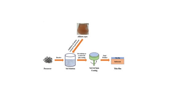
The 3 mm thick FTO glass substrate is first cut to the right size of 10 mm × 20 mm. It is then washed with detergent and deionized water, acetone, and ethanol. The glass substrate is afterward sonicated for 10 min in ethanol to remove any residual contaminants on the glass substrate and subsequently dried in nitrogen gas. The sol-gel synthesis of copper oxide thin film was achieved with a modified method previously reported by Krishnaprabha et al. [10]. In this study, CuSO4·5H2O was utilized as copper precursor while Allium cepa was adopted as the reducing agent for the synthesis of copper oxide. The waste peels of Allium cepa were sheared into smaller pieces and then placed in de-ionized water (15 g/30 mL), boiled, cooled, and afterward filtrated to obtain the filtrate. The CuO thin film was created using a sol-gel method which involved adding 10 mL of the plant extract to a strenuously stirred 30 mL aqueous solution of CuSO4·5H2O (0.1 M). This resulted in the solution illustrated in Figure 1. The mixture was then aged for 24 h and thereafter deposited on a very clean glass substrate by employing a spin coater unit set to 1000 and 3000 rpm for 10 and 30 s respectively. This was to enhance the uniform dispersion of the solution well over the substrate and for the formation of the thin film. The film was subsequently annealed at 400 °C for 3 h. The reaction temperature of 400 °C adopted for this study was a result of the findings from the existing works of Krishnaprabha et al. [10] and Johan et al. [32], which stated that the properties possessed by CuO thin films are unfavorable when the annealing temperature is below 400 °C.
2.3. Materials Characterization
The elemental composition together with the surface morphology of the produced thin film was analyzed with the use of SEM/EDS (TESCAN VEGA 3 TC SEM with an Oxford Energy Dispersive Spectrometer manufactured by TESCAN in Brno Czech Republic). XRD analysis (PANalytical X’Pert PRO X-ray Diffractometer using Cu radiation with K Beta filter, manufactured by PANalytical in Almelo, Netherlands) was carried out on the film to determine the structural qualities of the manufactured film. FTIR (IRAffinity-1S Fourier Transform Infrared Spectroscopy manufactured by Shimadzu in Kyoto, Japan) was conducted to study the chemical bonds possessed by the formed thin film. The UV-Vis transmittance and absorbance spectra were executed using the UV-1800 spectrophotometer to detect the amount of light the film can transmit and absorb, while the conductivity of the film was deduced with the Four Probe measurement (Four Probe-Resistivity Measurement SK012 manufactured by Indosaw in Ambala cantonment, India).
3. Results and Discussion
3.1. Scanning Electron Microscope (SEM) Analysis
The scanning electron microscope is a piece of excellent equipment for studying the surface morphology of thin films because it provides essential information on the sizes and shapes of particles. Previous research works have shown that the surface morphology of transparent conducting oxide (TCO) films has an impact on both the optical and electrical characteristics of the films, which are both important aspects in the application of optoelectronic devices. For instance, increased film surface roughness lowers the performance of solar cell photovoltaics, hence the need to study the surface morphology of thin films [33]. The morphological and structural features of the CuO film (Figure 2) which were deposited on a glass substrate and heat-treated at 400 °C for 3 h, were examined using the SEM analysis. The image from the SEM analysis displayed significant interparticle porosities which allowed the passage of vapor [34]. However, the size of the synthesized material (16.7 nm) is still within the nanometer range, but with a non-homogenous structure [35], while the film thickness was calculated to be 106.4 nm similar to previous studies of Lai et al. [36], Shariffudin et al. [37], and Lee & Wang [38]. From the SEM micrograph, it is obvious that the synthesized CuO was majorly composed of spherical agglomerates of CuO nanoparticles [39]. In general, the obtained results correspond to those of previous studies of [34,35,39,40,41,42], which was also demonstrated by the Energy Dispersive X-ray (EDX) analysis in the subsequent section that the synthesized material was solely CuO.
3.2. Elemental Analysis
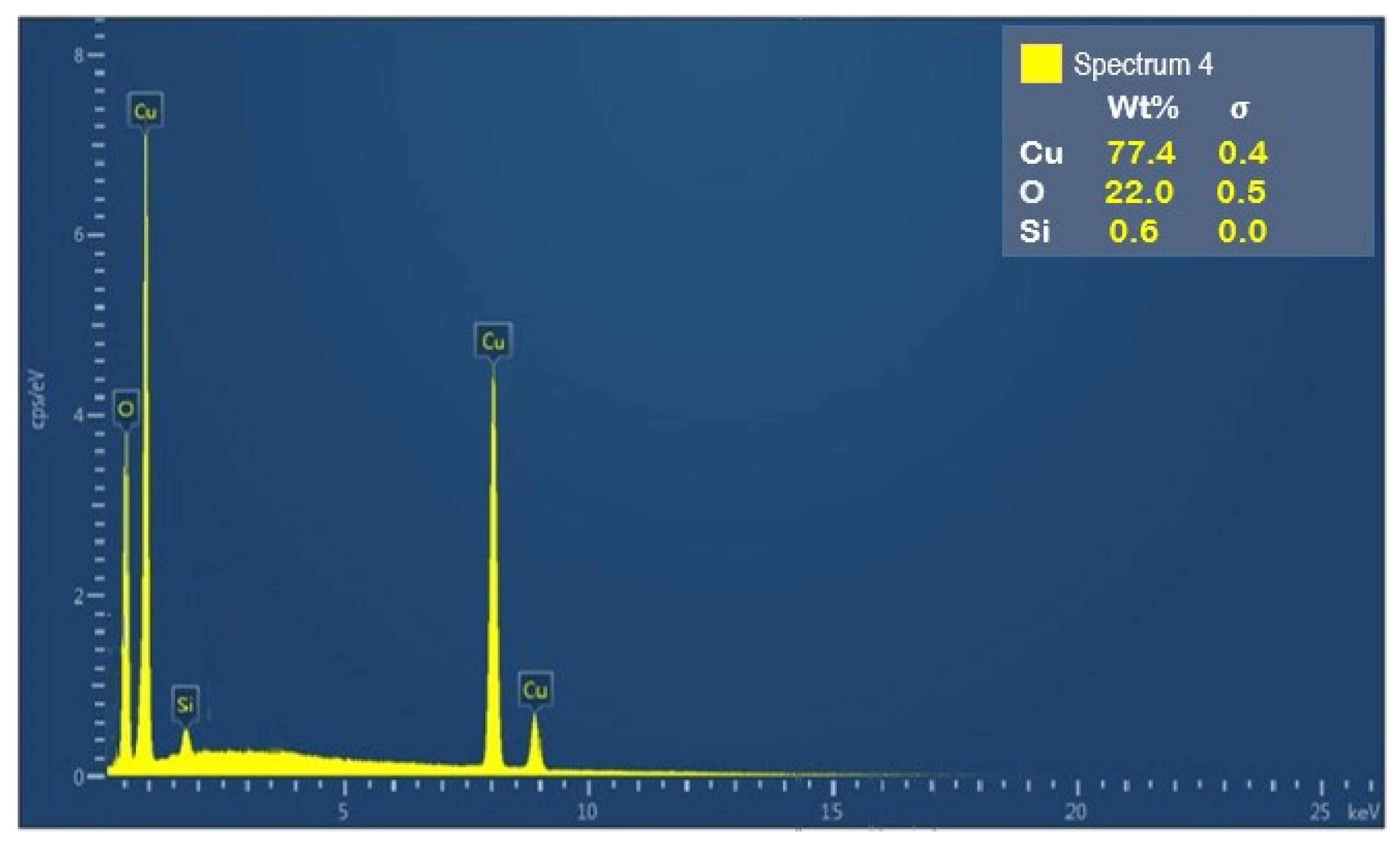
With the application of the energy-dispersive X-rays (EDX), the elemental composition and the purity of the produced CuO thin film calcined at 400 °C were studied. Depicted in Figure 3 is the EDX spectrum of the CuO thin film to affirm the occurrence of Cu and O in the prepared sample, as well as to analyze the chemical formation of the deposited material. The EDX spectrum illustrated in the figure confirms the existence of the constituent elements of silicon (Si), oxygen (O), and copper (Cu) in the synthesized CuO thin film. The silicon (Si) peak which was noticed from the figure originated from the glass substrate used for the deposition process which was made from silicon material [43]. Apparently, from the EDX pattern in Figure 3, it can be confirmed that CuO thin film was successfully formed from CuSO4·5H2O. The peak locations from the EDX spectrum showed consistency with CuO [35]. No other peaks were observed in the EDX spectrum which confirmed the production of pure CuO thin film on the glass substrate [39]. Thus, the aqueous Allium cepa leaf extract was discovered to be a strong eco-friendly reducing agent for reducing metal salts to their nanostructures. These discoveries are consistent with prior studies [35,44], but with minor variations owing to the changes in the chemical composition. Although the EDX analysis shows the elemental composition of the fabricated film, there is still the need for the structural properties of the synthesized film to be examined. This is to precisely ascertain the crystalline phase of the formed thin film.
3.3. X-ray Diffraction Analysis (XRD)
The crystalline structure of the fabricated copper oxide thin films was characterized by X-ray diffraction (XRD) (PANalytical X’Pert PRO X-ray Diffractometer) using Cu K α radiation (λ = 1.5406 A°) in the 2θ range start position of 4° and end position of 90° at 40 kV, 40 mA. All the observed diffraction peaks in Figure 4 can be indexed in the monoclinic phase with the unique 2θ diffraction peaks of, 32.51°, 35.43°, 38.70°, 46.27°,48.77°, 53.47°,58.24°, 61.55°,65.79°, 66.26°,67.86°,68.08° and 72.46° being attributed to (110), (002), (111), (−112), (−202), (020), (202), (−113), (022), (−311), (113), (220), and (311) lattice planes, respectively. These values agree with those previously reported as well as on the corresponding “JCPDS” (Joint Committee on Powder Diffraction Standards) card No. 45-0937 [45,46]. In addition, the average size of the crystallite was determined by adopting the Debye–Scherrer equation [47,48].
where ‘λ’ is defined as the wavelength of X-ray (0.154060 nm), ‘β’ is the FWHM known as the full width at half maximum, ‘θ’ is the angle of diffraction, and “D’ is crystallite size. The average crystallite size estimated with the Scherrer equation was 16.7 nm.
This thus was in close relation with the crystallite size of CuO powder in Manjunath et al. [49] and Buazar et al. [50] which were 8 and 20.76 nm, respectively, which was within the ideal crystallite nanometer range of less than 50 nm. However, the existence of stress in thin films and functional coatings poses a key problem in several technological applications because high levels of residual stress may significantly influence the performance, durability, and reliability of material components and devices [51]. Residual stresses can have a major effect on the adhesion and fracture strength of thin films, on the ductility of bulk metallic glasses [52], the performance of the optoelectronic components, and the lifespan of microelectromechanical systems (MEMS) and nanoelectromechanical (NEMS) [53]. On the other hand, stress may also improve the physical characteristics of nanostructures and thin layers, such as conductivity, piezoelectricity, dielectric permittivity, and magnetic anisotropy. It can also increase the mobility of charge carriers in silicon-based semiconducting technologies [54]. Consequently, the obtained results from this study corroborated with the EDX results of previous sections which revealed that the fabricated thin film consisted of only CuO.
3.4. Fourier Transform Infrared Analysis (FTIR)
One effective approach to examine the vibrational frequencies of specific bonds in a molecule is Fourier transform infrared analysis (FTIR). The prepared copper oxide thin film was scanned at room temperature within 4000 cm−1–400 cm−1 as revealed from the FTIR spectrum displayed in Figure 5. The observed peaks at 453 cm−1, 531 cm−1, 608 cm−1 correlate to the characteristic Cu-O bond stretching vibration of CuO [32,55]. Moreover, the absence of peaks at 605 and 660 cm−1 completely rule out the possibility of another phase, namely, Cu2O [56]. Furthermore, the appearance of peaks at 531 and 1051 cm−1 clearly shows various modes of bending vibration associated with the Cu–O bond while the presence of the peak at 1669 cm−1 also confirms the stretching vibration of the Cu–O bond [57]. The exclusion of peaks above 3000 cm−1 which represents the O–H stretching vibrations of H2O reveals that water molecules were not adsorbed [58]. Hence, the vibrational peaks from this study which represent the existing phase of the FTIR analysis also corroborate with the XRD peaks of the pure phase CuO, thus defining its monoclinic phase occurrence.
3.5. Uv-Vis Absorbance
As a result of the combined oscillation of free band conductive electrons which get excited from incident electromagnetic radiations due to the absorption of visible light, surface plasmon absorption (SPA) can be observed in metal oxides [10]. To comprehend the effect of light absorption on the CuO thin film, the optical properties of the film were analyzed with the use of the UV-Vis diffuse absorbance spectra (DRS). Illustrated in Figure 6 is the UV-Vis absorption spectrum of CuO thin film produced at 400 °C, at wavelengths ranging between 300 nm to 800 nm. The absorption peak of the CuO thin film was typically discovered at 390 nm like in previous related literature [30,59,60,61]. However, a widening absorption peak moving towards an increasing short visible wavelength region (400–600 nm) was observed in the sample, which is attributable to the intrinsic bandgap of CuO [62]. In addition, the absorbance around 565 nm (Figure 6) has been recognized in CuO systems as an indication of SPA [63,64]. The figure reveals the center of the SPA peak (565 nm) to have moved to higher absorbance with an increase in the wavelength, thus exhibiting a redshift. These illustrations thus state that the amount of light the film can absorb and the SPR peak location is dependent on the SEM analysis (shape and size) of the thin film. From Figure 6, the CuO absorption spectrum is noticed to have a sloping background caused by interband transitions [64,65]. Therefore, with reference to the figure, it can be said that the synthesized CuO strongly absorbs at the entire visible spectrum with minimal transparency for nanostructured samples of bigger band gaps, which can absorb in the UV region [66].
3.6. Band Gap
With the UV-V is absorption spectrophotometer being utilized to analyze how much light the CuO thin film is capable of absorbing, the initial absorption which conforms with the electron excitation from the valence band to the conduction band is adopted to deduce the optical band gap value of the manufactured film. In other words, the Tauc plot is employed for the calculation of the energy bandgap of the CuO thin film. (eV). The relationship which binds the absorption coefficient (α) and the incident photon energy (hυ) together can be written as,
where Eg = bandgap energy, α = absorption coefficient, K= proportionality constant, and hυ = energy of the incident photon, with n = 2 for a direct bandgap and n = ½ for an indirect bandgap.
αhυ = K (hυ − Eg)n
The bandgap is determined from the manipulation of the slope-intercept from the graph of (αhυ)2 versus hυ. A straight line as displayed in Figure 7 is derived when (αhυ)2 against hυ (eV) is plotted, which denotes that a direct allowed transition is responsible for the absorption edge. The optical band gap (Eg) is obtained at the point where the straight line intercepts the hυ axis. The optical band gap value for the copper oxide thin film (Figure 7) obtained from the sol-gel spin coating deposition approach is evaluated to be 1.48 eV, which is in accordance with the stated range of 1.21 eV to 1.51 eV for copper oxide (CuO) [17,32,67]. This reduced bandgap may have resulted from an increase in the thickness of the CuO thin film [68], which thus increases the possibility of the thin film being applied as an absorber layer in the fabrication of solar cells [69].
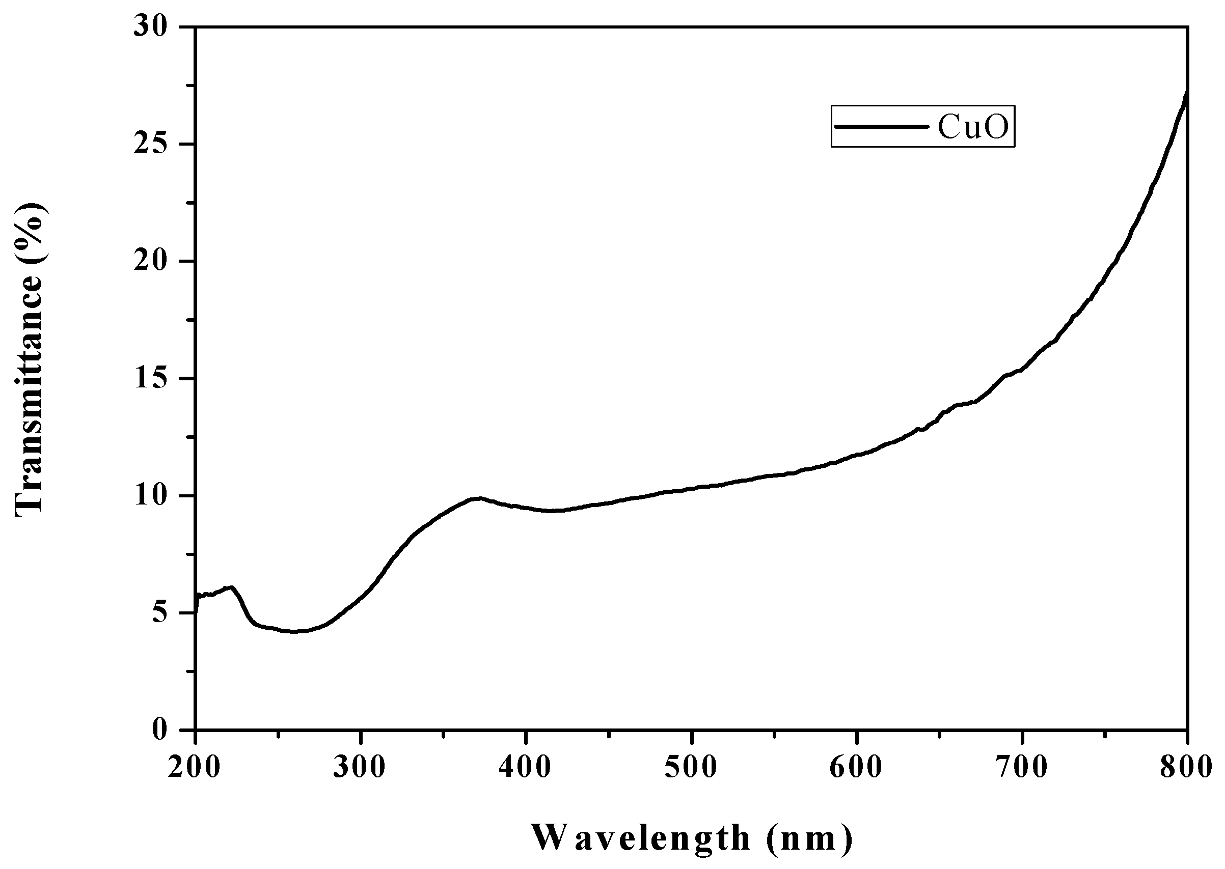
3.7. UV-Vis Transmittance
Presented in Figure 8 is the optical transmittance of the spin-coated CuO thin films in the spectral range of 200 nm to 800 nm achieved through the UV-Vis spectrometer. Generally, materials that display wide band-gap energies are known to have excellent transmittance, while those exhibiting low bandgap energies possess inferior transmittance, as is the case in this study. Furthermore, the film crystallinity, energy bandgap, and surface morphology are all influential on the transmittance of thin films [70].
From the plot (Figure 8), the film transmits effectively in the visible range than at the UV region. However, the coating at the entirety of the visible wavelength region was of low transparency, revealing an optical transmittance value of less than 30% [71,72], with a characteristic adsorption edge around the 350 nm region which could be attributed to the band edge of the CuO phase [72,73]. This decrease in transmittance experienced by the thin film may have resulted from the scattering of light at the coarse surface [71,74]. This result thus corroborates with the low energy band gap of 1.48 eV derived from the CuO thin film in the previous section.
3.8. Electrical Properties
Conductivity
The electrical conductivity of the CuO thin film was determined with the utilization of the four-point probe technique. The electrical conductivity of p-type CuO films varies with copper vacancy density, which acts as shallow acceptors [75]. The fabricated CuO thin film was revealed to be of intrinsic p-type semiconducting behavior which was probably a result of increasing copper deficiencies [76]. Revealed in Figure 9 is the electrical conductivity as a function of temperature for the CuO thin film. The figure showed that a temperature increase resulted in a significant conductivity increase of the annealed nanocrystalline CuO thin film which arose from an increase in the hole concentration, similar to previous findings of [77,78], with this conductivity pattern related to prior studies of [79,80]. Besides the annealing temperature, the increase in the electrical conductivity which was observed in this study can also be attributed to the film’s structure and texture, [81,82,83]. Thus, it is possible to tune the electrical properties of CuO by changing the stoichiometry and crystallinity of the CuO sample during the deposition process [84,85].
4. Conclusions
Synthesis of CuO thin film using Allium cepa extract as the reducing agent has been demonstrated in this study. By the utilization of a naturally existing plant, Allium cepa (aqueous extract) as the reducing agent, copper oxide nanoparticles were formed and accumulated into nanospheres. Peculiar IR bands at 453, 531, and 608 cm−1 indicated the formation of the Cu-O stretching vibrations. The crystalline structure and morphology studies carried out by the XRD, and SEM analysis demonstrated that the synthesized CuO thin film was of a monoclinic phase and was also spherically shaped. The fabricated CuO thin film was without impurities as illustrated by the EDX analysis. The UV-Vis spectroscopy revealed that the fabricated thin film absorbed and transmitted strongly at the entire visible wavelength regions with minimal and low transparencies respectively. While the estimated bandgap indicated that the produced thin film exhibited traits of a good conductor. Similarly, the electrical analysis revealed that the manufactured film possessed excellent electrical properties. In future, this environmentally friendly green approach of producing CuO thin films can be expanded towards the production of other significant industrial metal oxides. Furthermore, future studies can take into consideration the optimization of the parameters of temperature and concentration, to develop and improve on the findings that have been achieved from this study.
Author Contributions
Conceptualization, Formal Analysis, and Writing of the original draft of the article, E.C.N.; Reviewing, Validation, and editing of the article, P.E.I.; Formal Analysis and, Editing of the article, S.O.B.; Conceptualization, Resources, Reviewing & Editing, Supervision, T.-C.J. All authors have read and agreed to the published version of the manuscript.
Funding
This research received no external funding.
Institutional Review Board Statement
Not applicable.
Informed Consent Statement
Not applicable.
Data Availability Statement
Not applicable.
Acknowledgments
The authors herewith dedicate acknowledgment to the National Research Foundation (NRF) South Africa, the Global Excellence Stature (GES), and the University Research Commission (URC) for being supportive financially.
Conflicts of Interest
The authors declare no conflict of interest.
References
- Nandan, D.; Zoppellaro, G.; Medřík, I.; Aparicio, C.; Kumar, P.; Petr, M.; Tomanec, O.; Gawande, M.B.; Varma, R.S.; Zbořil, R. Cobalt-entrenched N-, O-, and S-tridoped carbons as efficient multifunctional sustainable catalysts for base-free selective oxidative esterification of alcohols. Green Chem. 2018, 20, 3542–3556. [Google Scholar] [CrossRef]
- Dhaouadi, M.; Jlassi, M.; Sta, I.; Miled, I.B.; Mousdis, G.; Kompitsas, M.; Dimassi, W. Physical properties of copper oxide thin films prepared by sol–gel spin–coating method. Am. J. Phys. Appl. 2018, 6, 43–50. [Google Scholar] [CrossRef] [Green Version]
- Mistry, V.H.; Mistry, B.V.; Modi, B.; Joshi, U. Effect of annealing on pulse laser deposition grown copper oxide thin film. AIP Conf. Proc. 2017, 1837, 040070. [Google Scholar]
- Asadi, M.; Rozati, S. Optical and structural properties of nanostructured copper oxide thin films as solar selective coating prepared by spray pyrolysis method. Mater. Sci. Pol. 2017, 35, 355–361. [Google Scholar] [CrossRef] [Green Version]
- Prabu, R.D.; Valanarasu, S.; Ganesh, V.; Shkir, M.; AlFaify, S.; Kathalingam, A.; Srikumar, S.; Chandramohan, R. An effect of temperature on structural, optical, photoluminescence and electrical properties of copper oxide thin films deposited by nebulizer spray pyrolysis technique. Mater. Sci. Semicond. Process. 2018, 74, 129–135. [Google Scholar] [CrossRef]
- Aghayan, M.; Hussainova, I.; Kirakosyan, K.; Rodríguez, M.A. The template-assisted wet-combustion synthesis of copper oxide nanoparticles on mesoporous network of alumina nanofibers. Mater. Chem. Phys. 2017, 192, 138–146. [Google Scholar]
- ÖZMENTEŞ, R. Effect of thermal annealing time on the optical characteristics of CuO thin films. Yüzüncü Yıl Üniversitesi Fen Bilimleri Enstitüsü Derg 2019, 24, 176–182. [Google Scholar]
- Mikami, K.; Kido, Y.; Akaishi, Y.; Quitain, A.; Kida, T. Synthesis of Cu2O/CuO nanocrystals and their application to H2S sensing. Sensors 2019, 19, 211. [Google Scholar] [CrossRef] [Green Version]
- Mazhir, S.N.; Yasen, H.; Salih, M.M.; Mohamed, G.H. Structural and solar cell properties of CuO doped TiO2 thin films prepared by laser induced plasma. J. Eng. Appl. Sci. 2018, 13, 3555–3561. [Google Scholar]
- Krishnaprabha, M.; Venu, M.P.; Pattabi, M. Copper oxide thin films anchored on glass substrate by sol gel spin coating technique. AIP Conf. Proc. 2018, 1953, 100075. [Google Scholar]
- Nakate, U.T.; Lee, G.H.; Ahmad, R.; Patil, P.; Hahn, Y.-B.; Yu, Y.; Suh, E.-k. Nano-bitter gourd like structured CuO for enhanced hydrogen gas sensor application. Int. J. Hydrogen Energy 2018, 43, 22705–22714. [Google Scholar] [CrossRef]
- Xu, Z.; Buehler, M.J. Hierarchical nanostructures are crucial to mitigate ultrasmall thermal point loads. Nano Lett. 2009, 9, 2065–2072. [Google Scholar] [CrossRef]
- Paladugu, M.; Zou, J.; Guo, Y.N.; Zhang, X.; Joyce, H.J.; Gao, Q.; Tan, H.H.; Jagadish, C.; Kim, Y. Formation of hierarchical InAs nanoring/GaAs nanowire heterostructures. Angew. Chem. Int. Ed. 2009, 48, 780–783. [Google Scholar] [CrossRef] [PubMed]
- Wang, X.; Hu, C.; Liu, H.; Du, G.; He, X.; Xi, Y. Synthesis of CuO nanostructures and their application for nonenzymatic glucose sensing. Sens. Actuators B Chem. 2010, 144, 220–225. [Google Scholar] [CrossRef]
- Kim, J.; Park, J.; Park, K. CuO hollow nanostructures catalyze [3 + 2] cycloaddition of azides with terminal alkynes. Chem. Commun. 2010, 46, 439–441. [Google Scholar]
- Ray, S.C. Preparation of copper oxide thin film by the sol–gel-like dip technique and study of their structural and optical properties. Sol. Energy Mater. Sol. Cells 2001, 68, 307–312. [Google Scholar] [CrossRef]
- Oral, A.; Menşur, E.; Aslan, M.; Başaran, E. The preparation of copper (II) oxide thin films and the study of their microstructures and optical properties. Mater. Chem. Phys. 2004, 83, 140–144. [Google Scholar] [CrossRef]
- Mårtensson, N. Optical properties of silica-copper oxide thin films prepared by spin coating. Appl. Opt. 2011, 42. Available online: http://www.diva-portal.org/smash/get/diva2:445710/FULLTEXT02.pdf (accessed on 23 November 2021).
- Kumar, D.A.; Xavier, F.P.; Shyla, J.M. Investigation on the variation of conductivity and photoconductivity of CuO thin films as a function of layers of coating. Arch. Appl. Sci. Res. 2012, 4, 2174–2183. [Google Scholar]
- Xiang, J.; Tu, J.; Zhang, L.; Zhou, Y.; Wang, X.; Shi, S. Self-assembled synthesis of hierarchical nanostructured CuO with various morphologies and their application as anodes for lithium ion batteries. J. Power Sources 2010, 195, 313–319. [Google Scholar] [CrossRef]
- Nair, M.; Guerrero, L.; Arenas, O.L.; Nair, P. Chemically deposited copper oxide thin films: Structural, optical and electrical characteristics. Appl. Surf. Sci. 1999, 150, 143–151. [Google Scholar] [CrossRef]
- Yu, L.; Zhang, G.; Wu, Y.; Bai, X.; Guo, D. Cupric oxide nanoflowers synthesized with a simple solution route and their field emission. J. Cryst. Growth 2008, 310, 3125–3130. [Google Scholar] [CrossRef]
- Teng, F.; Yao, W.; Zheng, Y.; Ma, Y.; Teng, Y.; Xu, T.; Liang, S.; Zhu, Y. Synthesis of flower-like CuO nanostructures as a sensitive sensor for catalysis. Sens. Actuators B 2008, 134, 761–768. [Google Scholar] [CrossRef]
- Das, S.K.; Khan, M.M.R.; Guha, A.K.; Naskar, N. Bio-inspired fabrication of silver nanoparticles on nanostructured silica: Characterization and application as a highly efficient hydrogenation catalyst. Green Chem. 2013, 15, 2548–2557. [Google Scholar] [CrossRef]
- Al-Gaashani, R.; Radiman, S.; Tabet, N.; Daud, A.R. Synthesis and optical properties of CuO nanostructures obtained via a novel thermal decomposition method. J. Alloys Compd. 2011, 509, 8761–8769. [Google Scholar]
- Nwanna, E.C.; Imoisili, P.E.; Jen, T.-C. Fabrication and synthesis of SnO X thin films: A review. Int. J. Adv. Manuf. Technol. 2020, 111, 2809–2831. [Google Scholar] [CrossRef]
- Boudrioua, A.; Chakaroun, M.; Fischer, A. An Introduction to Organic Lasers; Elsevier: Amsterdam, The Netherlands, 2017. [Google Scholar]
- Gawande, M.B.; Goswami, A.; Felpin, F.-X.; Asefa, T.; Huang, X.; Silva, R.; Zou, X.; Zboril, R.; Varma, R.S. Cu and Cu-based nanoparticles: Synthesis and applications in catalysis. Chem. Rev. 2016, 116, 3722–3811. [Google Scholar] [CrossRef] [Green Version]
- Devi, H.S.; Singh, T.D. Synthesis of copper oxide nanoparticles by a novel method and its application in the degradation of methyl orange. Adv. Electron. Electr. Eng. 2014, 4, 83–88. [Google Scholar]
- Naika, H.R.; Lingaraju, K.; Manjunath, K.; Kumar, D.; Nagaraju, G.; Suresh, D.; Nagabhushana, H. Green synthesis of CuO nanoparticles using Gloriosa superba L. extract and their antibacterial activity. J. Taibah Univ. Sci. 2015, 9, 7–12. [Google Scholar] [CrossRef] [Green Version]
- Khodashenas, B.; Ghorbani, H.R. Synthesis of copper nanoparticles: An overview of the various methods. Korean J. Chem. Eng. 2014, 31, 1105–1109. [Google Scholar] [CrossRef]
- Johan, M.R.; Suan, M.S.M.; Hawari, N.L.; Ching, H.A. Annealing effects on the properties of copper oxide thin films prepared by chemical deposition. Int. J. Electrochem. Sci 2011, 6, 6094–6104. [Google Scholar]
- Yıldırım, M.A.; Ateş, A. Influence of films thickness and structure on the photo-response of ZnO films. Opt. Commun. 2010, 283, 1370–1377. [Google Scholar] [CrossRef]
- Bonnot, K.; Doblas, D.; Schnell, F.; Schlur, L.; Spitzer, D. Chip calorimetry for the sensitive identification of hexogen and pentrite from their decomposition inside copper oxide nanoparticles. Anal. Chem. 2015, 87, 9494–9499. [Google Scholar] [CrossRef]
- Ijaz, F.; Shahid, S.; Khan, S.A.; Ahmad, W.; Zaman, S. Green synthesis of copper oxide nanoparticles using Abutilon indicum leaf extract: Antimicrobial, antioxidant and photocatalytic dye degradation activitie. Trop. J. Pharm. Res. 2017, 16, 743–753. [Google Scholar] [CrossRef] [Green Version]
- Lai, G.; Lan, H.; Lin, S.; Qu, Y.; Lai, F. Optical properties of the oxidation of Cu thin films prepared by thermal evaporation. Surf. Rev. Lett. 2013, 20, 1350011. [Google Scholar] [CrossRef]
- Shariffudin, S.; Khalid, S.; Sahat, N.; Sarah, M.; Hashim, H. Preparation and characterization of nanostructured CuO thin films using sol-gel dip coating. IOP Conf. Ser. Mater. Sci. Eng. 2015, 99, 012007. [Google Scholar]
- Lee, W.-J.; Wang, X.-J. Structural, optical, and electrical properties of copper oxide films grown by the silar method with post-annealing. Coatings 2021, 11, 864. [Google Scholar] [CrossRef]
- Prasad, K.S.; Patra, A.; Shruthi, G.; Chandan, S. Aqueous extract of Saraca indica leaves in the synthesis of copper oxide nanoparticles: Finding a way towards going green. J. Nanotechnol. 2017, 2017, 7502610. [Google Scholar] [CrossRef]
- Monadi, N.; Saeednia, S.; Iranmanesh, P.; Ardakani, M.H.; Sinaei, S. Preparation and characterization of copper oxide nanoparticles through solid state thermal decomposition of an aqua nitrato copper (II) complex with a tridentate schiff-base ligand as a new precursor. Nanosci. Nanotechnol.-Asia 2019, 9, 92–100. [Google Scholar]
- Saghatforoush, L.A.; Mehdizadeh, R.; Chalabian, F. Synthesis of CuO nanoparticles from a new nano-structured copper (II) Schiff base complex by ultrasonic and solvothermal methods: Structural, thermal and antibacterial studies. J. Chem. Pharm. Res. 2011, 3, 691–702. [Google Scholar]
- Dzhardimalieva, G.I.; Uflyand, I.E. Design and synthesis of coordination polymers with chelated units and their application in nanomaterials science. RSC Adv. 2017, 7, 42242–42288. [Google Scholar] [CrossRef] [Green Version]
- Ergin, B.; Ketenci, E.; Atay, F. Characterization of ZnO films obtained by ultrasonic spray pyrolysis technique. Int. J. Hydrogen Energy 2009, 34, 5249–5254. [Google Scholar] [CrossRef]
- Ren, G.; Hu, D.; Cheng, E.W.; Vargas-Reus, M.A.; Reip, P.; Allaker, R.P. Characterisation of copper oxide nanoparticles for antimicrobial applications. Int. J. Antimicrob. Agents 2009, 33, 587–590. [Google Scholar] [CrossRef]
- Joint Committee for Powder Diffraction Standards. Powder Diffraction File No. 01-087-0712; JCPDS International Center for Diffraction Data: Swarthmore, PA, USA, 1991. [Google Scholar]
- Volanti, D.; Keyson, D.; Cavalcante, L.; Simões, A.Z.; Joya, M.; Longo, E.; Varela, J.A.; Pizani, P.; Souza, A. Synthesis and characterization of CuO flower-nanostructure processing by a domestic hydrothermal microwave. J. Alloys Compd. 2008, 459, 537–542. [Google Scholar] [CrossRef]
- Caroling, G.; Priyadharshini, M.N.; Vinodhini, E.; Ranjitham, A.M.; Shanthi, P. Biosynthesis of copper nanoparticles using aqueous guava extract-characterisation and study of antibacterial effects. Int. J. Pharm. Biol. Sci. 2015, 5, 25–43. [Google Scholar]
- Mittu, R. Synthesis, characterization of copper nanoparticles-a review. Int. Adv. Res. J. Sci. Eng. Technol. 2016, 3, 37–40. [Google Scholar]
- Manjunath, A.; Irfan, M.; Anushree, K.P.; Vinutha, K.M.; Yamunarani, N. Synthesis and characterization of CuO nanoparticles and CuO doped PVA nanocomposites. Adv. Mater. Phys. Chem. 2016, 6, 263. [Google Scholar] [CrossRef] [Green Version]
- Buazar, F.; Sweidi, S.; Badri, M.; Kroushawi, F. Biofabrication of highly pure copper oxide nanoparticles using wheat seed extract and their catalytic activity: A mechanistic approach. Green Process. Synth 2019, 8, 691–702. [Google Scholar] [CrossRef]
- Mariello, M.; Fachechi, L.; Guido, F.; De Vittorio, M. Multifunctional sub-100 µm thickness flexible piezo/triboelectric hybrid water energy harvester based on biocompatible AlN and soft parylene C-PDMS-Ecoflex™. Nano Energy 2021, 83, 105811. [Google Scholar] [CrossRef]
- Zhang, Y.; Wang, W.; Greer, A. Making metallic glasses plastic by control of residual stress. Nat. Mater. 2006, 5, 857. [Google Scholar]
- Espinosa, H.; Prorok, B.; Fischer, M. A methodology for determining mechanical properties of freestanding thin films and MEMS materials. J. Mech. Phys. Solids 2003, 51, 47–67. [Google Scholar]
- Lee, M.L.; Fitzgerald, E.A.; Bulsara, M.T.; Currie, M.T.; Lochtefeld, A. Strained Si, SiGe, and Ge channels for high-mobility metal-oxide-semiconductor field-effect transistors. J. Appl. Phys. 2005, 97, 1. [Google Scholar] [CrossRef]
- Bodade, A.; Taiwade, M.; Chaudhari, G. Bioelectrode based chitosan-nano copper oxide for application to lipase biosensor. J. Appl. Pharm. Res. 2017, 5, 30–39. [Google Scholar]
- Zheng, L.; Liu, X. Solution-phase synthesis of CuO hierarchical nanosheets at near-neutral pH and near-room temperature. Mater. Lett. 2007, 61, 2222–2226. [Google Scholar] [CrossRef]
- Raul, P.K.; Senapati, S.; Sahoo, A.K.; Umlong, I.M.; Devi, R.R.; Thakur, A.J.; Veer, V. CuO nanorods: A potential and efficient adsorbent in water purification. RSC Adv. 2014, 4, 40580–40587. [Google Scholar] [CrossRef]
- Bitire, S.O.; Jen, T.-C.; Belaid, M. Transesterification of parsley seed oil using a green catalyst: Considering the optimization process and modeling. Int. J. Sustain. Energy 2021, 40, 977–1001. [Google Scholar] [CrossRef]
- Iqbal, J.; Jan, T.; Ul-Hassan, S.; Ahmed, I.; Mansoor, Q.; Umair Ali, M.; Abbas, F.; Ismail, M. Facile synthesis of Zn doped CuO hierarchical nanostructures: Structural, optical and antibacterial properties. AIP Adv. 2015, 5, 127112. [Google Scholar] [CrossRef] [Green Version]
- Khalid, A.; Ahmad, P.; Alharthi, A.I.; Muhammad, S.; Khandaker, M.U.; Rehman, M.; Faruque, M.R.I.; Din, I.U.; Alotaibi, M.A.; Alzimami, K. Structural, optical and antibacterial efficacy of pure and zinc-doped copper oxide against pathogenic bacteria. Nanomaterials 2021, 11, 451. [Google Scholar] [CrossRef]
- Butte, S.; Waghuley, S. Optical properties of Cu2O and CuO. AIP Conf. Proc. 2020, 2220, 020093. [Google Scholar]
- Dubale, A.A.; Pan, C.-J.; Tamirat, A.G.; Chen, H.-M.; Su, W.-N.; Chen, C.-H.; Rick, J.; Ayele, D.W.; Aragaw, B.A.; Lee, J.-F. Heterostructured Cu2O/CuO decorated with nickel as a highly efficient photocathode for photoelectrochemical water reduction. J. Mater. Chem. A 2015, 3, 12482–12499. [Google Scholar] [CrossRef]
- Wang, H.; Tam, F.; Grady, N.K.; Halas, N.J. Cu nanoshells: Effects of interband transitions on the nanoparticle plasmon resonance. J. Phys. Chem. B 2005, 109, 18218–18222. [Google Scholar] [CrossRef]
- Marimuthu, A.; Zhang, J.; Linic, S. Tuning selectivity in propylene epoxidation by plasmon mediated photo-switching of Cu oxidation state. Science 2013, 339, 1590–1593. [Google Scholar] [CrossRef] [PubMed] [Green Version]
- Cheng, Y.; Lin, Y.; Xu, J.; He, J.; Wang, T.; Yu, G.; Shao, D.; Wang, W.-H.; Lu, F.; Li, L. Surface plasmon resonance enhanced visible-light-driven photocatalytic activity in Cu nanoparticles covered Cu2O microspheres for degrading organic pollutants. Appl. Surf. Sci. 2016, 366, 120–128. [Google Scholar] [CrossRef]
- Jillani, S.; Jelani, M.; Hassan, N.U.; Ahmad, S.; Hafeez, M. Synthesis, characterization and biological studies of copper oxide nanostructures. Mater. Res. Express 2018, 5, 045006. [Google Scholar] [CrossRef]
- Yoon, K.H.; Choi, W.J.; Kang, D.H. Photoelectrochemical properties of copper oxide thin films coated on an n-Si substrate. Thin Solid Films 2000, 372, 250–256. [Google Scholar] [CrossRef]
- Ashour, A.; Kaid, M.; El-Sayed, N.; Ibrahim, A. Physical properties of ZnO thin films deposited by spray pyrolysis technique. Appl. Surf. Sci. 2006, 252, 7844–7848. [Google Scholar] [CrossRef]
- Wanjala, K.; Njoroge, W.; Ngaruiya, J. Optical and electrical characterization of ZnS: Sn thin films for solar cell application. Int. J. Energy Eng. 2016, 6, 1–7. [Google Scholar]
- Choi, D.-w.; Park, J.-S. Highly conductive SnO2 thin films deposited by atomic layer deposition using tetrakis-dimethyl-amine-tin precursor and ozone reactant. Surf. Coat. Technol. 2014, 259, 238–243. [Google Scholar] [CrossRef]
- Keikhaei, M.; Ichimura, M. Fabrication of Copper Oxide thin films by galvanostatic deposition from weakly acidic solutions. Int. J. Electrochem. Sci. 2018, 13, 9931–9941. [Google Scholar] [CrossRef]
- Farhad, S.F.U.; Hossain, M.A.; Tanvir, N.I.; Akter, R.; Patwary, M.A.M.; Shahjahan, M.; Rahman, M.A. Structural, optical, electrical, and photoelectrochemical properties of cuprous oxide thin films grown by modified SILAR method. Mater. Sci. Semicond. Process. 2019, 95, 68–75. [Google Scholar] [CrossRef]
- Farhad, S.F.U. Copper Oxide Thin Films Grown by Pulsed Laser Deposition for Photovoltaic Applications. Ph.D. Thesis, University of Bristol, Bristol, UK, 2016. [Google Scholar]
- Beena, D.; Lethy, K.; Vinodkumar, R.; Pillai, V.M.; Ganesan, V.; Phase, D.; Sudheer, S. Effect of substrate temperature on structural, optical and electrical properties of pulsed laser ablated nanostructured indium oxide films. Appl. Surf. Sci. 2009, 255, 8334–8342. [Google Scholar] [CrossRef]
- Meyer, B.; Polity, A.; Reppin, D.; Becker, M.; Hering, P.; Klar, P.; Sander, T.; Reindl, C.; Benz, J.; Eickhoff, M. Binary copper oxide semiconductors: From materials towards devices. Phys. Status Solidi B 2012, 249, 1487–1509. [Google Scholar] [CrossRef]
- Jeong, Y.K.; Choi, G.M. Nonstoichiometry and electrical conduction of CuO. J. Phys. Chem. Solids 1996, 57, 81–84. [Google Scholar] [CrossRef]
- Gopalakrishna, D.; Vijayalakshmi, K.; Ravidhas, C. Effect of annealing on the properties of nanostructured CuO thin films for enhanced ethanol sensitivity. Ceram. Int. 2013, 39, 7685–7691. [Google Scholar] [CrossRef]
- Suda, S.; Fujitsu, S.; Koumoto, K.; Yanagida, H. The effect of atmosphere and doping on electrical conductivity of CuO. Jpn. J. Appl. Phys. 1992, 31, 2488. [Google Scholar] [CrossRef]
- Kamble, D.L.; Harale, N.S.; Patil, V.L.; Patil, P.S.; Kadam, L.D. Characterization and NO2 gas sensing properties of spray pyrolyzed SnO2 thin films. J. Anal. Appl. Pyrolysis 2017, 127, 38–46. [Google Scholar] [CrossRef]
- Choi, G.; Satyanarayana, L.; Park, J. Effect of process parameters on surface morphology and characterization of PE-ALD SnO2 thin films for gas sensing. Appl. Surf. Sci. 2006, 252, 7878–7883. [Google Scholar] [CrossRef]
- Shao, P.; Deng, S.; Chen, J.; Chen, J.; Xu, N. Study of field emission, electrical transport, and their correlation of individual single CuO nanowires. J. Appl. Phys. 2011, 109, 023710. [Google Scholar] [CrossRef]
- Zhang, Q.; Zhang, K.; Xu, D.; Yang, G.; Huang, H.; Nie, F.; Liu, C.; Yang, S. CuO nanostructures: Synthesis, characterization, growth mechanisms, fundamental properties, and applications. Prog. Mater Sci. 2014, 60, 208–337. [Google Scholar] [CrossRef]
- Musselman, K.P.; Marin, A.; Schmidt-Mende, L.; MacManus-Driscoll, J.L. Incompatible length scales in nanostructured Cu2O solar cells. Adv. Funct. Mater. 2012, 22, 2202–2208. [Google Scholar] [CrossRef] [Green Version]
- Zoolfakar, A.S.; Rani, R.A.; Morfa, A.J.; O’Mullane, A.P.; Kalantar-Zadeh, K. Nanostructured copper oxide semiconductors: A perspective on materials, synthesis methods and applications. J. Mater. Chem. C 2014, 2, 5247–5270. [Google Scholar] [CrossRef] [Green Version]
- Viet Pham, T.; Rao, M.; Andreasson, P.; Peng, Y.; Wang, J.; Jinesh, K. Photocarrier generation in CuxO thin films deposited by radio frequency sputtering. Appl. Phys. Lett. 2013, 102, 032101. [Google Scholar] [CrossRef]
Figure 1.
Preparation procedure of CuO thin film using Allium cepa as reducing agent.
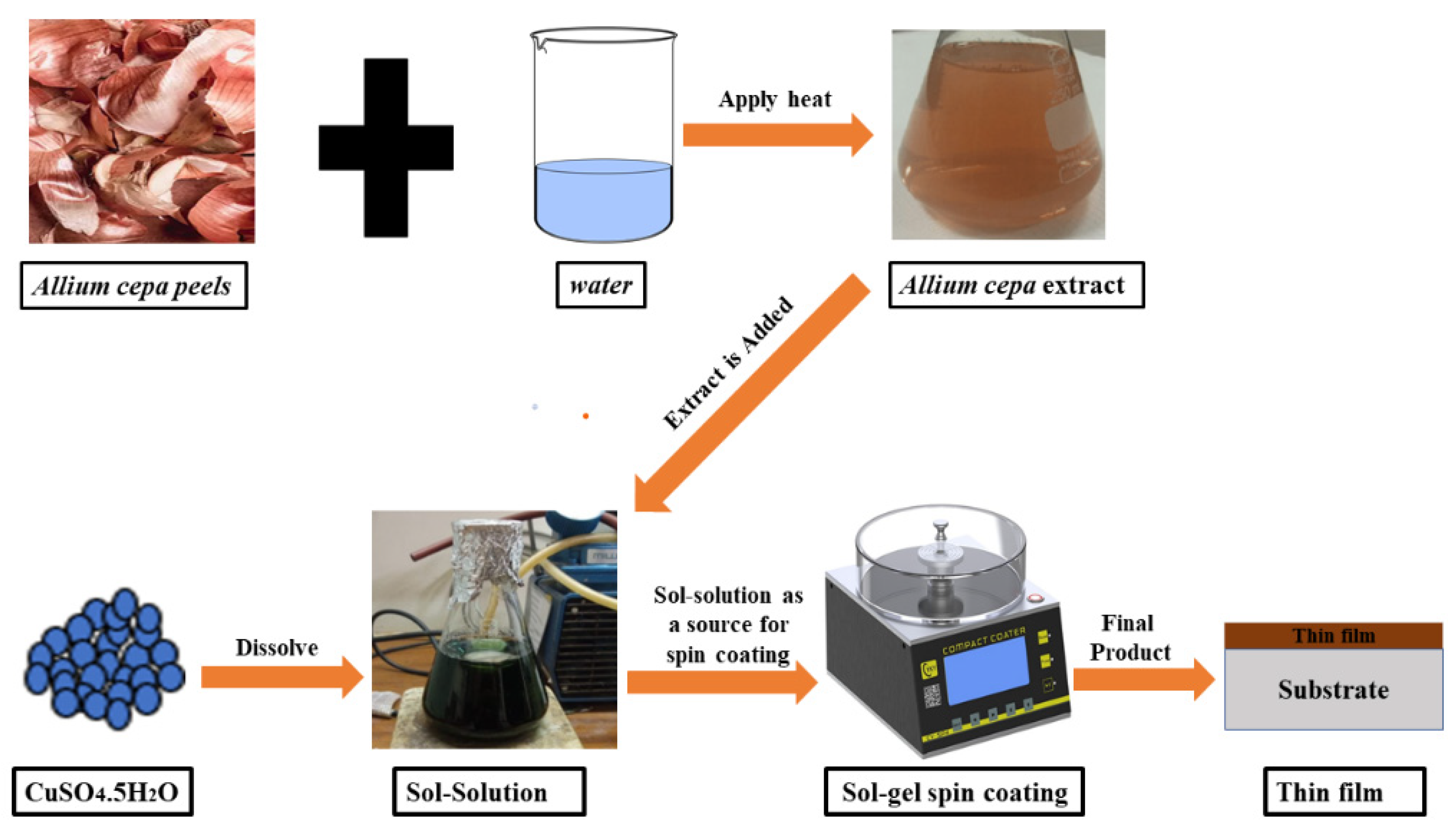
Figure 2.
SEM micrograph of CuO.

Figure 3.
EDX spectra of the CuO thin film.

Figure 4.
X-ray diffraction pattern of CuO thin film.
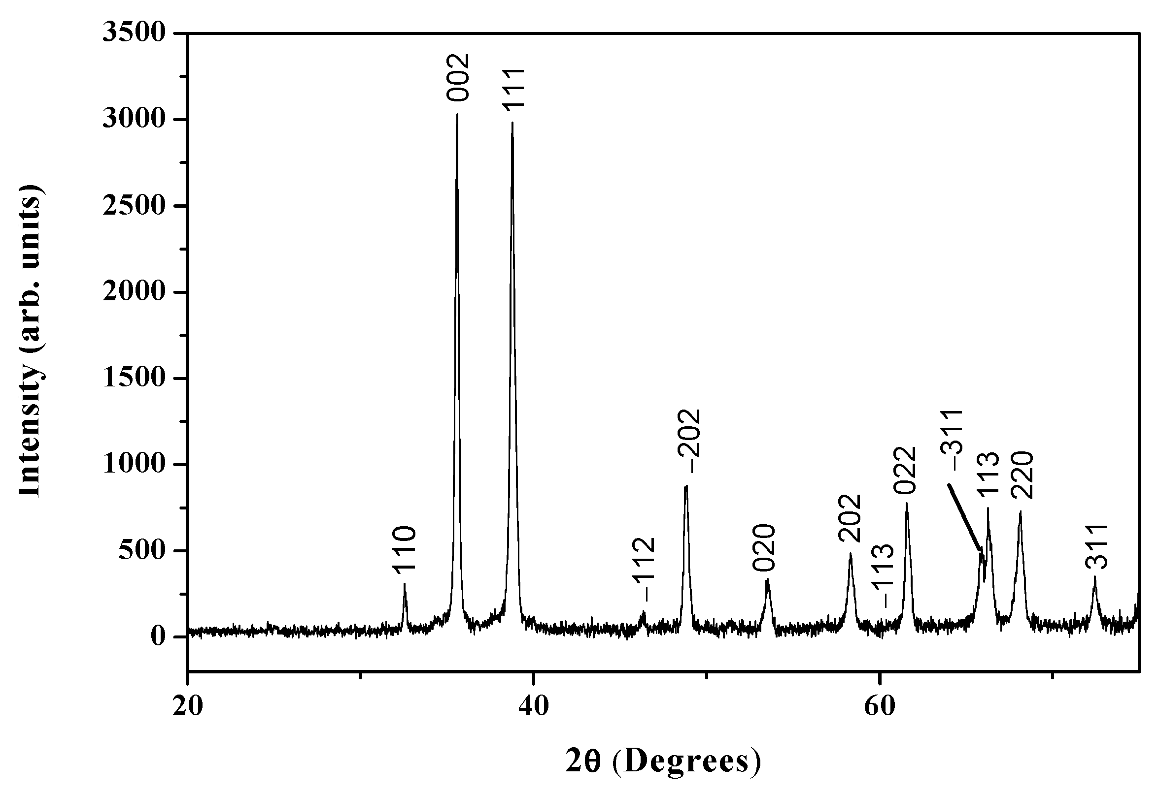
Figure 5.
FTIR spectra of CuO thin film.
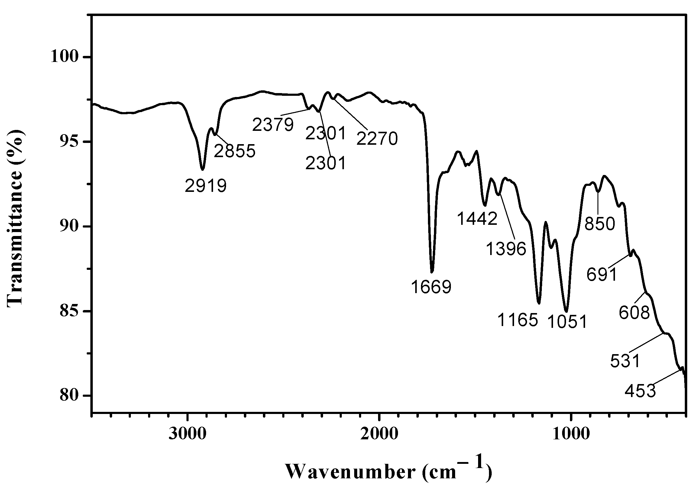
Figure 6.
The UV-visible absorption spectra of CuO thin film.

Figure 7.
The Bandgap of CuO thin film.
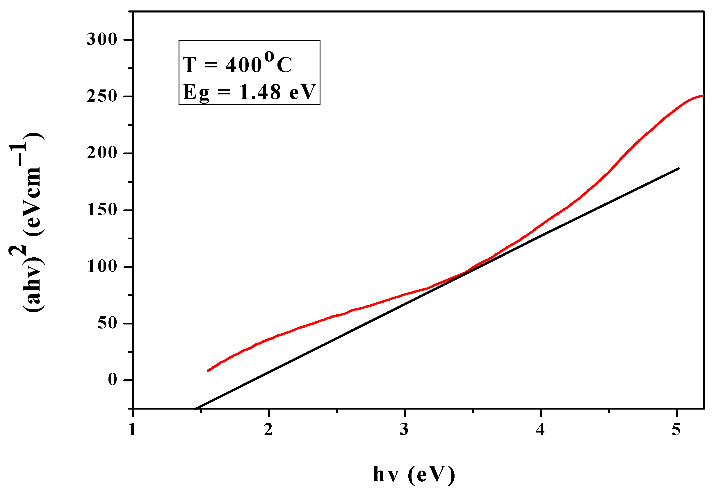
Figure 8.
The UV-Vis transmittance spectra of CuO thin film.

Figure 9.
The conductivity of CuO thin film.

Publisher’s Note: MDPI stays neutral with regard to jurisdictional claims in published maps and institutional affiliations. |
© 2021 by the authors. Licensee MDPI, Basel, Switzerland. This article is an open access article distributed under the terms and conditions of the Creative Commons Attribution (CC BY) license (https://creativecommons.org/licenses/by/4.0/).
Share and Cite
MDPI and ACS Style
Nwanna, E.C.; Imoisili, P.E.; Bitire, S.O.; Jen, T.-C. Biosynthesis and Fabrication of Copper Oxide Thin Films as a P-Type Semiconductor for Solar Cell Applications. Coatings 2021, 11, 1545. https://doi.org/10.3390/coatings11121545
AMA Style
Nwanna EC, Imoisili PE, Bitire SO, Jen T-C. Biosynthesis and Fabrication of Copper Oxide Thin Films as a P-Type Semiconductor for Solar Cell Applications. Coatings. 2021; 11(12):1545. https://doi.org/10.3390/coatings11121545
Chicago/Turabian StyleNwanna, Emeka Charles, Patrick Ehi Imoisili, Sarah Oluwabunmi Bitire, and Tien-Chien Jen. 2021. "Biosynthesis and Fabrication of Copper Oxide Thin Films as a P-Type Semiconductor for Solar Cell Applications" Coatings 11, no. 12: 1545. https://doi.org/10.3390/coatings11121545
Note that from the first issue of 2016, this journal uses article numbers instead of page numbers. See further details here.