
Electrode Materials for Flexible Electrochromics


Abstract
1. Introduction
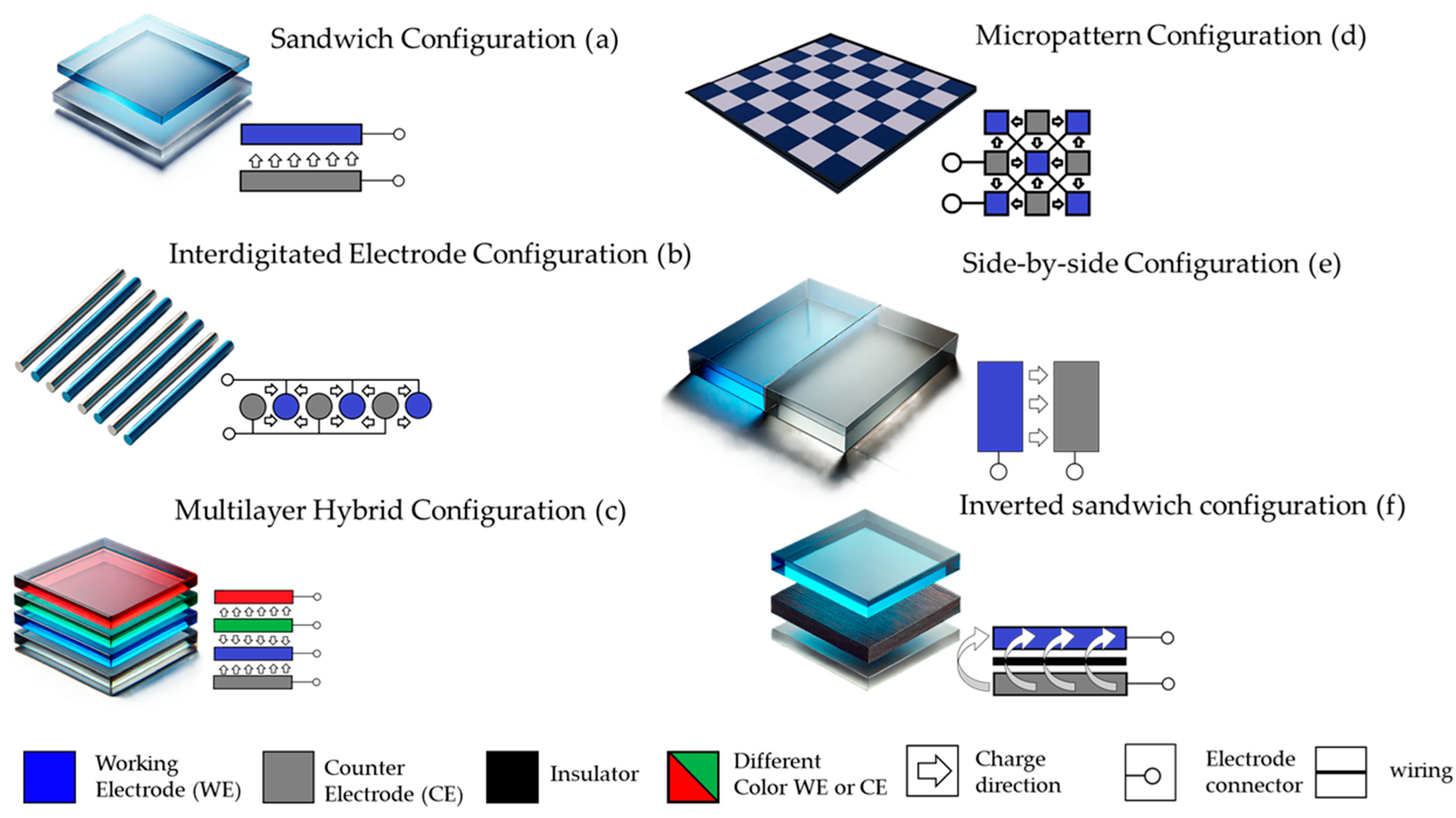
2. Flexible Electrochromic Devices Architecture
- -
- Sandwich Configuration: The sandwich ECD architecture represents the most conventional design in ECDs [28,29]. In this configuration, the device comprises sequentially stacked layers, including a transparent conductive electrode, an electrochromic layer, an electrolyte, and a counter electrode (Figure 2a). The transparent conductive electrode, often fabricated from indium tin oxide (ITO) or silver nanowires (AgNWs), serves as the base layer, ensuring electrical connectivity and optical transparency. The electrochromic layer, typically made of materials like tungsten oxide (WO3) [30] or PEDOT/PSS [31], modulates light transmission through reversible redox reactions. A solid, gel, or liquid electrolyte facilitates ion transport, while the counter electrode, such as nickel oxide (NiO) [32], balances ionic charges during device operation. This architecture is particularly suited for applications requiring high optical contrast and uniform coloration, such as smart windows and e-paper displays. Flexible and stretchable ECDs are designed to maintain functionality under mechanical deformation, including bending, stretching, and twisting. These devices utilize elastic substrates such as polydimethylsiloxane (PDMS) [33,34] or thermoplastic polyurethane (TPU) [35] in conjunction with flexible conductive electrodes like carbon nanotubes (CNTs) [36,37,38], graphene, or AgNWs [33,34]. The electrochromic materials are often embedded within or coated onto these substrates to ensure mechanical durability. This architecture is particularly suited for wearable electronics and biomedical applications, where flexibility and lightweight construction are essential. Despite its mechanical advantages, the lifespan of such devices may decrease under extreme deformation conditions [39]. Additionally, achieving a balance between flexibility and high optical modulation remains a challenge [40,41].
- -
- Interdigitated Electrode Configuration: The interdigitated configuration employs a patterned arrangement of electrochromic and counter-electrode materials in an alternating “finger-like” structure (Figure 2b) [42]. The gaps between the interdigitated fingers are filled with an electrolyte, enabling efficient ion transport. This design offers several advantages, including faster switching speeds and precise control over coloration due to the short ionic pathways between the electrodes. High-resolution displays and adaptive optical systems are among the primary applications for this architecture. The fabrication of interdigitated configurations requires advanced techniques such as lithography or high-precision printing, making it a costly option for large-scale production. Furthermore, maintaining uniformity across the patterned electrodes poses significant challenges.
- -
- Multilayer Hybrid Configuration: This architecture combines multiple functional materials and layers to achieve superior durability, optical modulation, and environmental resistance (Figure 2c) [43,44,45]. Devices constructed in this architecture often integrate inorganic and organic materials, such as WO3 combined with conductive polymers like PEDOT/PSS, to leverage the benefits of both material types [46,47,48]. This architecture is widely used in advanced displays and energy-efficient windows, where high durability and performance are paramount. However, the increased complexity of the fabrication process and the higher cost of materials may hinder widespread adoption.
- -
- Micropatterned Configuration: Micropatterning involves segmenting the electrochromic material into discrete regions or “pixels,” enabling localized control over optical modulation (Figure 2d) [49,50]. Advanced lithographic techniques or printing methods are used to create high-resolution patterns, making this architecture suitable for e-paper displays and adaptive optics. While micropatterned architectures offer unparalleled design flexibility, they require precise fabrication processes that can be expensive and time-intensive. Uniformity across patterns and scalability remains a significant hurdle for widespread application.
- -
- Side-by-Side Electrode Configuration: In the side-by-side configuration, both the electrochromic and counter electrodes are positioned laterally on the same substrate (Figure 2e) [51]. A thin electrolyte layer bridges the gap between the electrodes, facilitating ionic movement [52,53]. This architecture is particularly advantageous for thin and lightweight devices, as it eliminates the need for multiple stacked layers, reducing overall device thickness. While this design simplifies device structure, it inherently limits the coloration area due to the lateral positioning of the electrodes as the counter electrode often does not have any color change. Additionally, the longer ionic pathways between adjacent electrodes can lead to slower switching speeds compared to other architectures [54,55].
- -
- Reverse Sandwich Configuration: This alternative, also known as “inverted sandwich” architecture, is a lesser-used configuration in which the roles of certain layers are reversed, or non-transparent materials such as metal foils replace conventional transparent electrodes (Figure 2f) [56,57]. In this design, the electrochromic material is directly deposited onto the metal foil, which acts as both the electrode and the substrate. The electrolyte layer is subsequently applied, followed by a counter electrode positioned on the opposite side. This architecture is ideal for non-transparent applications, including smart mirrors and adaptive thermal shields, where optical transparency is not required. Stainless steel or aluminum foils often serve as substrates, providing exceptional mechanical durability and chemical stability [57,58]. Despite its simplified fabrication and robust mechanical properties, this architecture is not useful for see-through devices and may face challenges in achieving high optical contrast.
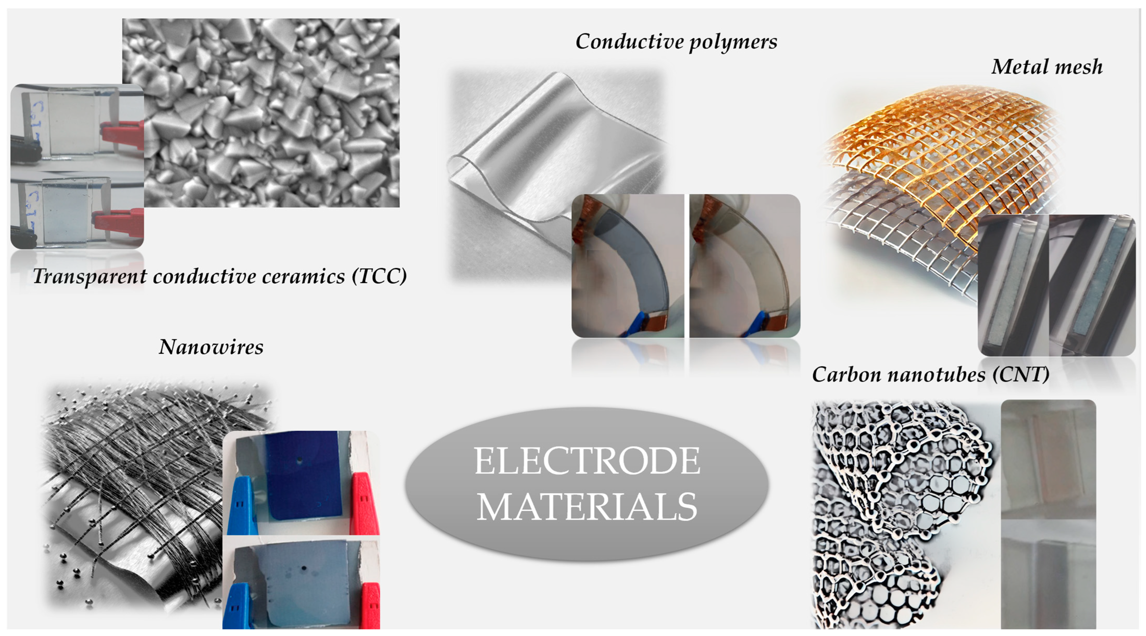
3. Electrodes in Flexible ECDs
3.1. Silver Nanowires
3.1.1. Manufacturing Methods of AgNW
- Spray Coating: A scalable method where the AgNW solution is sprayed onto the substrate, offering uniform coverage and compatibility with large-area devices [68].
- Spin Coating: Used for smaller-scale applications, this method ensures uniform thin films by spinning the substrate at high speeds. This method is commonly used in laboratories, as it provides precise and repeatable preparation of samples [69].
- Surface plasma treatment: Surface plasma treatment is a method that is generally used as a post-treatment to enhance the properties of AgNWs, particularly their electrical conductivity and adhesion to substrates. The material is first prepared by using one of the more common procedures and involves exposing AgNWs to a plasma, which helps to remove contaminants, oxide layers, or organic coatings. By reducing the insulating layer (e.g., PVP), plasma treatment lowers the contact resistance between nanowires, enhancing network conductivity [70].
- Electron beam lithography (EBL): This method uses a focused beam of electrons to directly write custom patterns. By focusing a beam of electrons onto a substrate coated with an electron-sensitive resist, EBL can directly write patterns without the need for masks, achieving resolutions below 10 nanometers [66].
3.1.2. Chemical Stability of AgNW
3.1.3. Durability of AgNW
3.1.4. Device Construction Capabilities of AgNW
3.2. Metal Meshes
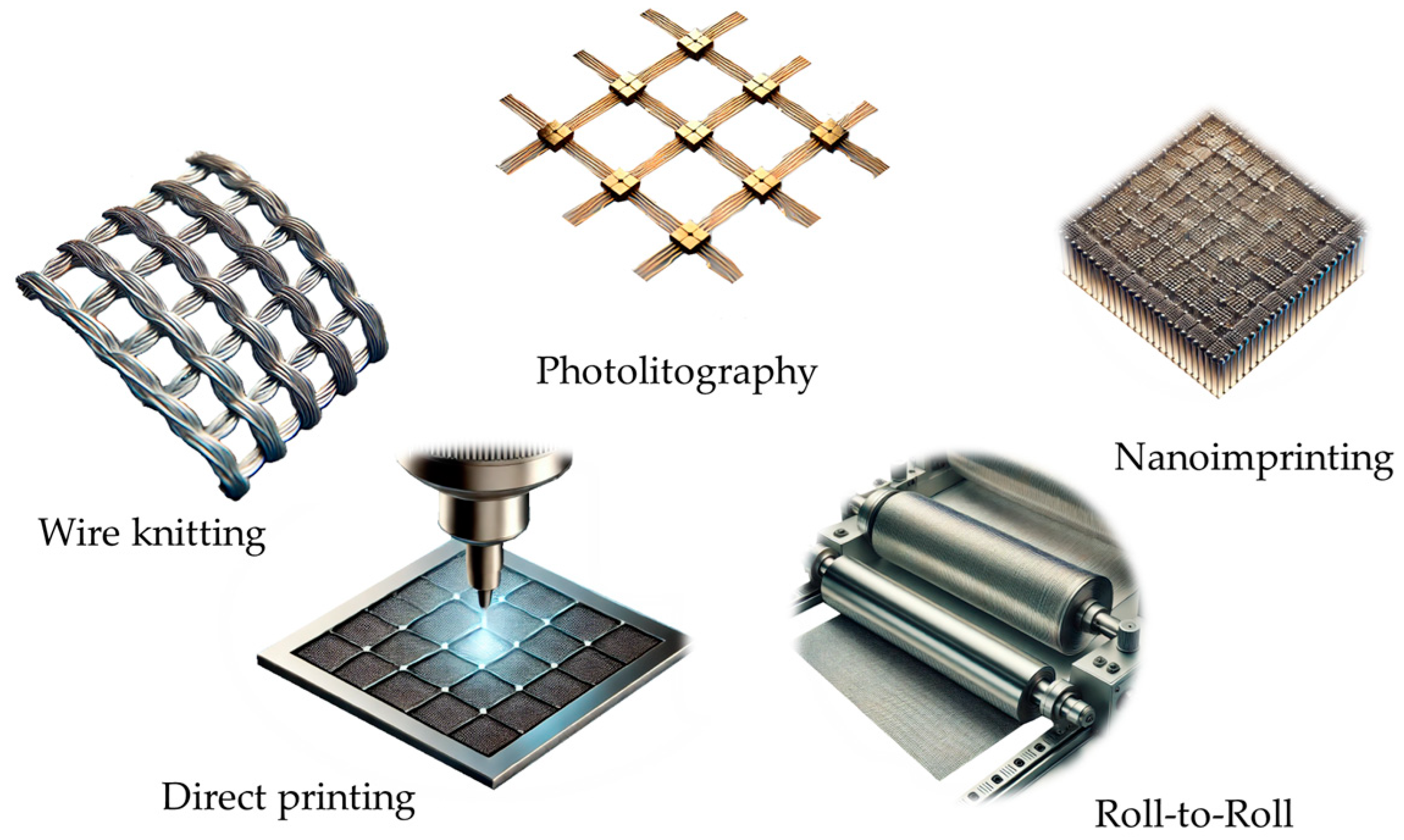
3.2.1. Manufacturing Methods of Metal Meshes
- Wire Knitting: Knitted wire mesh consists of a metal wire strand knitted into a mesh structure in very much the same way as thread is knitted into fabric [100].
- Photolithography: This method involves patterning a photosensitive layer on a metal-coated substrate using UV light. The unexposed areas are then etched away, leaving behind a fine mesh pattern. Photolithography provides high precision and is widely used for small-scale applications where fine resolution is critical [98].
- Nanoimprint Lithography: Nanoimprinting in general employs a mold or stamp to pattern the metal layer on a substrate. The specific method that is used for metal mesh production is nanoimprinting by capillary forces [101], which utilizes a metal-containing ink or precursor solution that is introduced by capillary action into the cavities between the mold and the substrate. Upon subsequent drying and annealing, well-defined metal mesh patterns are formed. This technique facilitates controlled deposition at nanoscale resolution that is compatible with flexible substrates. It enables manufacture of smaller devices or parts of devices, which can be used to manufacture a large number of devices or assemble the imprints in larger devices [102]. This cost-effective technique is suitable for large-scale production and enables the creation of nanoscale grid patterns that enhance optical transparency [103].
- Direct Printing: Techniques such as inkjet printing and aerosol jet printing allow the direct deposition of metal inks onto substrates [106]. These methods enable rapid prototyping and are compatible with various substrate types, including flexible polymers [107,108]. Recently, 3D printing has become an attractive method to prepare electrodes as well [109].
3.2.2. Chemical Stability of Metal Meshes
3.2.3. Durability of Metal Meshes
3.2.4. Device Construction Capabilities of Metal Meshes
3.3. Conductive Polymers
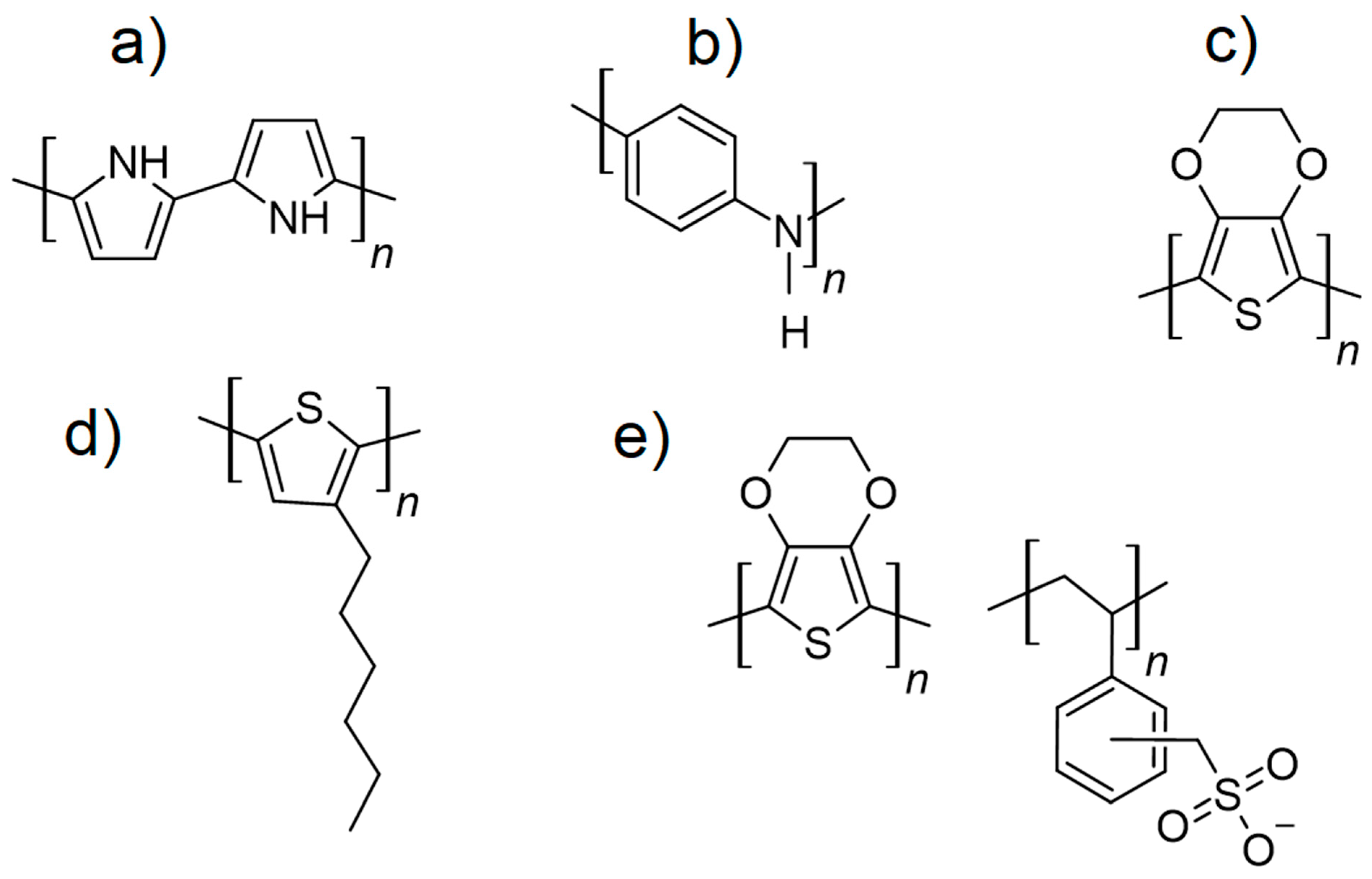
3.3.1. Poly(3,4-ethylenedioxythiophene)/Polystyrene Sulfonate (PEDOT/PSS)
3.3.2. Polyaniline (PANI)
3.3.3. Polypyrrole (PPy)
3.3.4. Polythiophenes (PTs)
3.3.5. Emerging TCPs and Specialized Materials
- Polyfluorenes: Known for their optical properties, polyfluorenes can be doped to achieve conductivity [138]. They are primarily used in research applications for light-emitting devices and flexible electronics.
- Poly(ethylene dioxythiophene-co-dioxythiophene) (PEDOT/DOT): A derivative of PEDOT, PEDOT/DOT provides enhanced transparency and electrical conductivity, making it suitable for advanced applications in flexible displays and wearable electronics [139].
3.3.6. Manufacturing Methods of Conductive Polymers
- Poly(3,4-ethylenedioxythiophene) Polystyrene Sulfonate (PEDOT/PSS)
- -
- Solution Processing: The material is dissolved in water or alcohol-based solvents to create a colloidal dispersion [141,147]. Further thin film preparation techniques include spin coating, spray coating, dip coating, and inkjet printing, which allow precise deposition on substrates of various sizes and shapes [148,149,150,151].
- -
- Electropolymerization: This method involves the electrochemical deposition of PEDOT on an electrode from a monomer solution [152]. This method enables controlled film thickness and uniformity.
- Polyaniline (PANI) and Polypyrrole (PPy)
- Polythiophenes (PTs)
3.3.7. Chemical Stability and Durability of Conductive Polymers
3.4. Carbon Nanotubes
3.4.1. Manufacturing Methods of CNTs
3.4.2. Chemical Stability and Durability of CNTs
3.5. Transparent Conductive Ceramics
3.5.1. Tin Oxide-Based Electrodes
- -
- Indium Tin Oxide (ITO): ITO is one of the most widely used transparent conductive oxides due to its exceptional optical transparency and electrical conductivity [192,193,194]. This material achieves low sheet resistance and high transmittance, making it ideal for applications such as ECDs, touchscreens, and displays. ITO’s ability to form thin, uniform films via techniques such as sputtering and chemical vapor deposition (CVD) further enhances its versatility. However, ITO faces significant challenges, including brittleness, which drastically restricts its use in flexible devices, and the high cost of indium, which limits its widespread use for more low-end applications [195]. ITO remains a benchmark material for transparent conductive ceramics in rigid optoelectronic devices and is in that regard often compared to other materials.
- -
- Fluorine-Doped Tin Oxide (FTO): FTO is among the most commonly used transparent conductive ceramics due to its high optical transparency and moderate electrical conductivity [193]. Its excellent stability under thermal and chemical stress makes it ideal for ECDs exposed to harsh environments. FTO is often used as a substrate for electrochromic coatings in smart windows and displays. However, its brittleness and high sheet resistance compared to materials like ITO limits its use in flexible applications.
- -
- Antimony-Doped Tin Oxide (ATO): ATO is another tin oxide-based material offering excellent stability and durability under UV exposure [193]. While its conductivity is slightly lower than that of FTO, it exhibits superior thermal resistance [196]. However, high processing costs and limited flexibility present challenges for broader adoption.
3.5.2. Zinc Oxide-Based Electrodes
- -
- Aluminum-Doped Zinc Oxide (AZO): AZO is a low-cost electrical alternative to indium-based TCOs like ITO. It combines high transparency and conductivity with good environmental stability [194]. AZO’s flexibility when deposited on polymer substrates makes it suitable for flexible ECDs and wearable devices [197]. However, AZO is susceptible to degradation under high humidity or UV exposure, necessitating protective coatings to maintain long-term performance [198].
- -
- Gallium-Doped Zinc Oxide (GZO): GZO provides comparable electrical conductivity and optical transparency to AZO but with enhanced chemical and thermal stability [199,200]. This makes GZO less prone to degradation, particularly in outdoor environments. As a result, it is frequently employed in applications such as smart windows and ECDs exposed to extreme conditions. Despite its advantages, GZO’s higher production cost compared to AZO can limit its widespread use.
3.5.3. Indium-Free Transparent Conductive Ceramics
3.5.4. Manufacturing Methods of TCCs
- -
- Indium Tin Oxide (ITO)
- ○
- Sputtering:
- ○
- Pulsed Laser Deposition (PLD):
- ○
- Chemical or Physical Vapor Deposition (CVD or PVD):
- -
- Fluorine-Doped Tin Oxide (FTO)
- ○
- Spray Pyrolysis:
- ○
- Chemical Vapor Deposition (CVD):
- ○
- Sputtering:
- -
- Aluminum-Doped Zinc Oxide (AZO)
- ○
- Sputtering:
- ○
- Chemical Vapor Deposition (CVD):
- ○
- Hydrothermal synthesis:
- ○
- Solution Processing:
4. Discussion
5. Conclusions
Author Contributions
Funding
Data Availability Statement
Acknowledgments
Conflicts of Interest
References
- Mortimer, R.J. Electrochromic materials. Annu. Rev. Mater. Res. 2011, 41, 241–268. [Google Scholar]
- Hamada, H.; Yano, K.; Take, H.; Inami, Y.; Matsuura, M.; Wada, T. Electrochromic displays: Status and future prospects. Displays 1983, 4, 221–225. [Google Scholar]
- Zhang, X.; Chang, D.; Liu, J.; Luo, Y. Conducting polymer aerogels from supercritical CO2 drying PEDOT-PSS hydrogels. J. Mater. Chem. 2010, 20, 5080–5085. [Google Scholar]
- Kao, S.-Y.; Lu, H.-C.; Kung, C.-W.; Chen, H.-W.; Chang, T.-H.; Ho, K.-C. Thermally cured dual functional viologen-based all-in-one electrochromic devices with panchromatic modulation. ACS Appl. Mater. Interfaces 2016, 8, 4175–4184. [Google Scholar]
- Ohsuku, T.; Hirai, T. An electrochromic display based on titanium dioxide. Electrochim. Acta 1982, 27, 1263–1266. [Google Scholar]
- Schmidt, D.J.; Pridgen, E.M.; Hammond, P.T.; Love, J.C. Layer-by-layer assembly of a ph-responsive and electrochromic thin film. J. Chem. Educ. 2010, 87, 208–211. [Google Scholar]
- Szmacinski, H.; Lakowicz, J.R. Fluorescence lifetime-based sensing and imaging. Sens. Actuators B Chem. 1995, 29, 16–24. [Google Scholar] [PubMed]
- Dalisa, A.L. Electrophoretic display technology. IEEE Trans. Electron Devices 1977, 24, 827–834. [Google Scholar]
- Kulesza, P.J.; Malik, M.A.; Zamponi, S.; Berrettoni, M.; Marassi, R. Electrolyte-cation-dependent coloring, electrochromism and thermochromism of cobalt(ii) hexacyanoferrate(iii, ii) films. J. Electroanal. Chem. 1995, 397, 287–292. [Google Scholar]
- Wang, C.; Li, J.; Zhang, L.; Fu, S. Preparation and property optimization of bistable electrochromic microcapsules. Dye. Pigment. 2022, 197, 109936. [Google Scholar]
- Sun, X.W.; Wang, J.X. Fast switching electrochromic display using a viologen-modified ZnO nanowire array electrode. Nano Lett. 2008, 8, 1884–1889. [Google Scholar] [PubMed]
- Granqvist, C.-G. Electrochromic metal oxides: An introduction to materials and devices. In Electrochromic Materials and Devices; Wiley: Hoboken, NJ, USA, 2013; pp. 1–40. [Google Scholar]
- Wen, H.; Weng, B.; Wang, B.; Xiao, W.; Liu, X.; Wang, Y.; Zhang, M.; Huang, H. Advancements in transparent conductive oxides for photoelectrochemical applications. Nanomaterials 2024, 14, 591. [Google Scholar] [CrossRef] [PubMed]
- Harris, K.D.; Elias, A.L.; Chung, H.J. Flexible electronics under strain: A review of mechanical characterization and durability enhancement strategies. J. Mater. Sci. 2016, 51, 2771–2805. [Google Scholar]
- Huang, S.; Liu, Y.; Zhao, Y.; Ren, Z.; Guo, C.F. Flexible electronics: Stretchable electrodes and their future. Adv. Funct. Mater. 2019, 29, 1805924. [Google Scholar]
- Huang, L.; Chen, X.; Wu, X.; Hu, Z.; Nie, S.; Huang, C.; Zhang, S.; Xu, W.; Pei, F.; Su, W.; et al. Hybrid Ag/Ni mesh/PH 1000 transparent electrodes for high performance flexible electrochromic devices with exceptional stability. Flex. Print. Electron. 2023, 8, 025021. [Google Scholar]
- Qiu, T.; Luo, B.; Liang, M.; Ning, J.; Wang, B.; Li, X.; Zhi, L. Hydrogen reduced graphene oxide/metal grid hybrid film: Towards high performance transparent conductive electrode for flexible electrochromic devices. Carbon 2015, 81, 232–238. [Google Scholar]
- Jung, J.; Cho, H.; Yuksel, R.; Kim, D.; Lee, H.; Kwon, J.; Lee, P.; Yeo, J.; Hong, S.; Unalan, H.E.; et al. Stretchable/flexible silver nanowire electrodes for energy device applications. Nanoscale 2019, 11, 20356–20378. [Google Scholar]
- Chen, J.; Minett, A.I.; Liu, Y.; Lynam, C.; Sherrell, P.; Wang, C.; Wallace, G.G. Direct growth of flexible carbon nanotube electrodes. Adv. Mater. 2008, 20, 566–570. [Google Scholar]
- Tan, R.K.L.; Reeves, S.P.; Hashemi, N.; Thomas, D.G.; Kavak, E.; Montazami, R.; Hashemi, N.N. Graphene as a flexible electrode: Review of fabrication approaches. J. Mater. Chem. A 2017, 5, 17777–17803. [Google Scholar]
- Das, T.K.; Prusty, S. Review on conducting polymers and their applications. Polym. Plast. Technol. Eng. 2012, 51, 1487–1500. [Google Scholar]
- Wang, J.; Jiu, J.; Araki, T.; Nogi, M.; Sugahara, T.; Nagao, S.; Koga, H.; He, P.; Suganuma, K. Silver nanowire electrodes: Conductivity improvement without post-treatment and application in capacitive pressure sensors. Nano-Micro Lett. 2015, 7, 51–58. [Google Scholar] [CrossRef] [PubMed]
- Spechler, J.A.; Koh, T.-W.; Herb, J.T.; Rand, B.P.; Arnold, C.B. A transparent, smooth, thermally robust, conductive polyimide for flexible electronics. Adv. Funct. Mater. 2015, 25, 7428–7434. [Google Scholar] [CrossRef]
- Jensen, J.; Hösel, M.; Dyer, A.L.; Krebs, F.C. Development and manufacture of polymer-based electrochromic devices. Adv. Funct. Mater. 2015, 25, 2073–2090. [Google Scholar] [CrossRef]
- Steinberg, M.D.; Kassal, P.; Steinberg, I.M. System architectures in wearable electrochemical sensors. Electroanalysis 2016, 28, 1149–1169. [Google Scholar] [CrossRef]
- Cai, G.; Wang, J.; Lee, P.S. Next-generation multifunctional electrochromic devices. Acc. Chem. Res. 2016, 49, 1469–1476. [Google Scholar] [CrossRef]
- Li, L.; Yu, Z.; Ye, C.; Song, Y. Structural color boosted electrochromic devices: Strategies and applications. Adv. Funct. Mater. 2024, 34, 2311845. [Google Scholar] [CrossRef]
- Deb, S.K. A novel electrophotographic system. Appl. Opt. 1969, 8, 192–195. [Google Scholar] [CrossRef]
- Chang, I.F.; Gilbert, B.L.; Sun, T.I. Electrochemichromic systems for display applications. J. Electrochem. Soc. 1975, 122, 955. [Google Scholar] [CrossRef]
- Deb, S.K.; Witzke, H. The solid state electrochromic phenomenon and its applications to display devices. In Proceedings of the 1975 International Electron Devices Meeting, Washington, DC, USA, 1–3 December 1975; pp. 393–397. [Google Scholar]
- Gustafsson, J.C.; Liedberg, B.; Inganäs, O. In situ spectroscopic investigations of electrochromism and ion transport in a poly (3,4-ethylenedioxythiophene) electrode in a solid state electrochemical cell. Solid State Ion. 1994, 69, 145–152. [Google Scholar] [CrossRef]
- Theodosiou, K.; Giannopoulos, P.; Georgakopoulos, T.; Stathatos, E. Quasi-solid-state electrochromic cells with energy storage properties made with inkjet printing. Materials 2020, 13, 3241. [Google Scholar] [CrossRef]
- Liu, H.-S.; Pan, B.-C.; Liou, G.-S. Highly transparent agnw/pdms stretchable electrodes for elastomeric electrochromic devices. Nanoscale 2017, 9, 2633–2639. [Google Scholar] [PubMed]
- Chen, W.-H.; Li, F.-W.; Liou, G.-S. Novel stretchable ambipolar electrochromic devices based on highly transparent AgNW/PDMS hybrid electrodes. Adv. Opt. Mater. 2019, 7, 1900632. [Google Scholar]
- Koo, J.; Amoli, V.; Kim, S.Y.; Lee, C.; Kim, J.; Park, S.-M.; Kim, J.; Ahn, J.M.; Jung, K.J.; Kim, D.H. Low-power, deformable, dynamic multicolor electrochromic skin. Nano Energy 2020, 78, 105199. [Google Scholar]
- Varghese Hansen, R.; Yang, J.; Zheng, L. Flexible electrochromic materials based on CNT/PDA hybrids. Adv. Colloid Interface Sci. 2018, 258, 21–35. [Google Scholar]
- Shi, G.; Fan, H.; Wang, W.; Hou, C.; Zhang, Q.; Li, Y.; Xiao, H.; Dai, G.; Li, K.; Wang, H. Carbon nanotube-grid infrared transparent electrodes for flexible electrochromic devices with visible to mid-infrared dual-band modulation. Mater. Today Chem. 2024, 39, 102166. [Google Scholar]
- Cao, X.; Lau, C.; Liu, Y.; Wu, F.; Gui, H.; Liu, Q.; Ma, Y.; Wan, H.; Amer, M.R.; Zhou, C. Fully screen-printed, large-area, and flexible active-matrix electrochromic displays using carbon nanotube thin-film transistors. ACS Nano 2016, 10, 9816–9822. [Google Scholar]
- Li, W.; Bai, T.; Fu, G.; Zhang, Q.; Liu, J.; Wang, H.; Sun, Y.; Yan, H. Progress and challenges in flexible electrochromic devices. Sol. Energy Mater. Sol. Cells 2022, 240, 111709. [Google Scholar]
- Nuroldayeva, G.; Balanay, M.P. Flexing the spectrum: Advancements and prospects of flexible electrochromic materials. Polymers 2023, 15, 2924. [Google Scholar] [CrossRef]
- Yu, J.; Wang, S.; Gao, L.; Qiao, G.; Lin, M.-F.; Wei, C.; Chen, J.; Li, S. Recent advances in flexible multifunctional electrochromic devices. Nanoscale 2025, 17, 6919–6937. [Google Scholar]
- Habboush, S.; Rojas, S.; Rodríguez, N.; Rivadeneyra, A. The role of interdigitated electrodes in printed and flexible electronics. Sensors 2024, 24, 2717. [Google Scholar] [CrossRef]
- Agrawal, V.; Ghosh, T.; Kumar, R.; Singla, E.; Agnihotri, P.K. Design and fabrication of dual electrochromic device with broader color space. J. Mater. Sci. Mater. Electron. 2024, 35, 1263. [Google Scholar] [CrossRef]
- Liang, Z.; Yukikawa, M.; Nakamura, K.; Kobayashi, N. A novel organic electrochromic device with hybrid capacitor architecture towards multicolour representation. Phys. Chem. Chem. Phys. 2018, 20, 19892–19899. [Google Scholar] [CrossRef]
- Bian, C.; Wang, J.; Liu, H.; Yan, Y.; Zhang, P.; Yang, W.; Jia, S.; Guo, X.; Cai, G. Complementary multicolor electrochromic devices with excellent stability based on porous tin oxide nanosheet scaffold. Nano Res. 2024, 17, 3035–3042. [Google Scholar] [CrossRef]
- Shinde, M.A.; Ahmad, K.; Kim, H. Fabrication of PEDOT:PSS/WO3 films on indium tin oxide based glass and flexible substrates for smart windows application. Opt. Mater. 2024, 149, 114980. [Google Scholar] [CrossRef]
- Gurudevi, P.; Venkateswari, P.; Sivakumar, T.; Ramesh, C.; Vanitha, P. Solution processed WO3 and PEDOT:PSS composite for hole transport layer in ITO-free organic solar cells. J. Clust. Sci. 2023, 34, 2135–2145. [Google Scholar] [CrossRef]
- Nie, S.; Ning, C.; Liu, Y.; Lian, Y.; Zhao, L.; Liu, Z. Enhanced electrochromic performance of WO3/PEDOT by π-electron conjugation system. Ceram. Int. 2024, 50, 12481–12488. [Google Scholar] [CrossRef]
- Lee, J.; Lee, Y.; Ahn, J.; Kim, J.; Yoon, S.; Kim, Y.S.; Cho, K.Y. Improved electrochromic device performance from silver grid on flexible transparent conducting electrode prepared by electrohydrodynamic jet printing. J. Mater. Chem. C 2017, 5, 12800–12806. [Google Scholar] [CrossRef]
- Jeong, S.-J.; Jo, M.-H.; Ahn, H.-J. 3D-printed film architecture via automatic micro 3D-printing system: Micro-intersection engineering of V2O5 thin/thick films for ultrafast electrochromic energy storage devices. Chem. Eng. J. 2023, 475, 146503. [Google Scholar] [CrossRef]
- Marques, A.; Santos, L.; Pereira, S.; Emanuele, U.; Sinopoli, S.; Igreja, R.; Sales, G.; Martins, R.; Fortunato, E. A planar electrochromic device using WO3 nanoparticles and a modified paper-based electrolyte. Proceedings 2018, 2, 1065. [Google Scholar] [CrossRef]
- Barquinha, P.; Pereira, S.; Pereira, L.; Wojcik, P.; Grey, P.; Martins, R.; Fortunato, E. Flexible and transparent WO3 transistor with electrical and optical modulation. Adv. Electron. Mater. 2015, 1, 1500030. [Google Scholar] [CrossRef]
- Grey, P.; Pereira, L.; Pereira, S.; Barquinha, P.; Cunha, I.; Martins, R.; Fortunato, E. Transistors: Solid state electrochemical WO3 transistors with high current modulation. Adv. Electron. Mater. 2016, 2, 1500414. [Google Scholar] [CrossRef]
- Deb, S.K. Opportunities and challenges in science and technology of WO3 for electrochromic and related applications. Sol. Energy Mater. Sol. Cells 2008, 92, 245–258. [Google Scholar] [CrossRef]
- Monk, P.; Mortimer, R.; Rosseinsky, D. (Eds.) A brief history of electrochromism. In Electrochromism and Electrochromic Devices; Cambridge University Press: Cambridge, UK, 2007; pp. 25–32. [Google Scholar]
- Rozman, M.; Gaberšček, M.; Marolt, G.; Bren, U.; Lukšič, M. An inverted sandwich electrochromic device architecture does not require optically transparent electrodes. Adv. Mater. Technol. 2019, 4, 1900389. [Google Scholar] [CrossRef]
- Zheng, J.Y.; Sun, Q.; Cui, J.; Yu, X.; Li, S.; Zhang, L.; Jiang, S.; Ma, W.; Ma, R. Review on recent progress in WO3-based electrochromic films: Preparation methods and performance enhancement strategies. Nanoscale 2023, 15, 63–79. [Google Scholar] [CrossRef]
- Rozman, M.; Žener, B.; Matoh, L.; Godec, R.F.; Mourtzikou, A.; Stathatos, E.; Bren, U.; Lukšič, M. Flexible electrochromic tape using steel foil with WO3 thin film. Electrochim. Acta 2020, 330, 135329. [Google Scholar] [CrossRef]
- Lu, H.-Y.; Chou, C.-Y.; Wu, J.-H.; Lin, J.-J.; Liou, G.-S. Highly transparent and flexible polyimide–AgNW hybrid electrodes with excellent thermal stability for electrochromic applications and defogging devices. J. Mater. Chem. C 2015, 3, 3629–3635. [Google Scholar] [CrossRef]
- Shinde, M.A.; Kim, H. Highly stable silver nanowire-based transparent conductive electrodes for electrochromic devices. Mater. Today Commun. 2021, 26, 102147. [Google Scholar] [CrossRef]
- Fisk, Z.; Webb, G.W. 5—Electrical resistivity of metals. In Treatise on Materials Science & Technology; Fradin, F.Y., Ed.; Elsevier: Amsterdam, The Netherlands, 1981; Volume 21, pp. 297–349. [Google Scholar]
- Lee, J.-Y.; Connor, S.T.; Cui, Y.; Peumans, P. Solution-processed metal nanowire mesh transparent electrodes. Nano Lett. 2008, 8, 689–692. [Google Scholar] [CrossRef]
- Zhang, W.; Chen, X.; Zhang, G.; Wang, S.; Zhu, S.; Wu, X.; Wang, Y.; Wang, Q.; Hu, C. Conducting polymer/silver nanowires stacking composite films for high-performance electrochromic devices. Sol. Energy Mater. Sol. Cells 2019, 200, 109919. [Google Scholar] [CrossRef]
- Xu, F.; Xu, W.; Mao, B.; Shen, W.; Yu, Y.; Tan, R.; Song, W. Preparation and cold welding of silver nanowire based transparent electrodes with optical transmittances >90% and sheet resistances < 10 ohm/sq. J. Colloid Interface Sci. 2018, 512, 208–218. [Google Scholar]
- Scardaci, V.; Coull, R.; Lyons, P.E.; Rickard, D.; Coleman, J.N. Spray deposition of highly transparent, low-resistance networks of silver nanowires over large areas. Small 2011, 7, 2621–2628. [Google Scholar] [PubMed]
- van de Groep, J.; Spinelli, P.; Polman, A. Transparent conducting silver nanowire networks. Nano Lett. 2012, 12, 3138–3144. [Google Scholar] [CrossRef]
- Hemmati, S.; Harris, M.T.; Barkey, D.P. Polyol silver nanowire synthesis and the outlook for a green process. J. Nanomater. 2020, 2020, 9341983. [Google Scholar] [CrossRef]
- Kim, T.; Canlier, A.; Kim, G.H.; Choi, J.; Park, M.; Han, S.M. Electrostatic spray deposition of highly transparent silver nanowire electrode on flexible substrate. ACS Appl. Mater. Interfaces 2013, 5, 788–794. [Google Scholar] [PubMed]
- Teymouri, Z.; Naji, L.; Fakharan, Z. The influences of polyol process parameters on the optoelectronic characteristics of AgNWs-based flexible electrodes and their application in ITO-free polymer solar cells. Org. Electron. 2018, 62, 621–629. [Google Scholar]
- Li, J.; Tao, Y.; Chen, S.; Li, H.; Chen, P.; Wei, M.-Z.; Wang, H.; Li, K.; Mazzeo, M.; Duan, Y. A flexible plasma-treated silver-nanowire electrode for organic light-emitting devices. Sci. Rep. 2017, 7, 16468. [Google Scholar]
- Kim, S.; Kim, S.Y.; Kim, J.; Kim, J.H. Highly reliable AGNW/PEDOT:PSS hybrid films: Efficient methods for enhancing transparency and lowering resistance and haziness. J. Mater. Chem. C 2014, 2, 5636–5643. [Google Scholar] [CrossRef]
- Liu, Y.-S.; Feng, J.; Ou, X.-L.; Cui, H.-F.; Xu, M.; Sun, H.-B. Ultrasmooth, highly conductive and transparent PEDOT:PSS/silver nanowire composite electrode for flexible organic light-emitting devices. Org. Electron. 2016, 31, 247–252. [Google Scholar]
- Ahn, Y.; Jeong, Y.; Lee, Y. Improved thermal oxidation stability of solution-processable silver nanowire transparent electrode by reduced graphene oxide. ACS Appl. Mater. Interfaces 2012, 4, 6410–6414. [Google Scholar] [CrossRef]
- Guan, F.; He, H.; Li, Q.; Shen, Y.; Kang, F.; Zhang, C.; Zhai, H. Transparent conductive films based on silver nanowires and SiO2 nanoparticles for flexible electronics. ACS Appl. Nano Mater. 2024, 7, 7845–7855. [Google Scholar]
- Ma, Y.; Sim, G.W.; Jo, S.; Hyun, D.C.; Roh, J.-S.; Ko, D.; Kim, J. Stability of silver-nanowire-based flexible transparent electrodes under mechanical stress. Appl. Sci. 2024, 14, 420. [Google Scholar] [CrossRef]
- Mayousse, C.; Celle, C.; Fraczkiewicz, A.; Simonato, J.-P. Stability of silver nanowire based electrodes under environmental and electrical stresses. Nanoscale 2015, 7, 2107–2115. [Google Scholar] [CrossRef] [PubMed]
- Yun, T.G.; Hwang, B. Effect of mechanical properties of substrates on flexibility of Ag nanowire electrodes under a large number of bending cycles. Coatings 2021, 11, 1074. [Google Scholar] [CrossRef]
- Hao, T.; Wang, S.; Xu, H.; Zhang, X.; Xue, J.; Liu, S.; Song, Y.; Li, Y.; Zhao, J. Highly robust, transparent, and conductive films based on AgNW-c nanowires for flexible smart windows. Appl. Surf. Sci. 2021, 559, 149846. [Google Scholar] [CrossRef]
- Ding, Y.; Cui, Y.; Liu, X.; Liu, G.; Shan, F. Welded silver nanowire networks as high-performance transparent conductive electrodes: Welding techniques and device applications. Appl. Mater. Today 2020, 20, 100634. [Google Scholar] [CrossRef]
- Lee, H.B.; Jin, W.-Y.; Ovhal, M.M.; Kumar, N.; Kang, J.-W. Flexible transparent conducting electrodes based on metal meshes for organic optoelectronic device applications: A review. J. Mater. Chem. C 2019, 7, 1087–1110. [Google Scholar] [CrossRef]
- Zhou, H.; Song, Y. Fabrication of silver mesh/grid and its applications in electronics. ACS Appl. Mater. Interfaces 2021, 13, 3493–3511. [Google Scholar] [CrossRef]
- Kim, W.-K.; Lee, S.; Hee Lee, D.; Hee Park, I.; Seong Bae, J.; Woo Lee, T.; Kim, J.-Y.; Hun Park, J.; Chan Cho, Y.; Ryong Cho, C.; et al. Cu mesh for flexible transparent conductive electrodes. Sci. Rep. 2015, 5, 10715. [Google Scholar] [CrossRef]
- Yavuz, A.; Kaplan, K.; Bedir, M. Copper oxide coated stainless steel mesh for flexible electrodes. J. Phys. Chem. Solids 2021, 150, 109824. [Google Scholar] [CrossRef]
- Kummer, M.; Kirchhoff, J.R. Graphite-coated metal mesh optically transparent electrodes. Anal. Chem. 1993, 65, 3720–3725. [Google Scholar] [CrossRef]
- Ali, M.M.; Hussain, A.; Song, R.-H.; Khan, M.Z.; Park, S.-J.; Ishfaq, H.A.; Joh, D.W.; Hong, J.-E.; Lee, S.-B.; Lim, T.-H. Beyond traditional fuel cells: Development and a comprehensive analysis of mechanically robust metal mesh-supported solid oxide fuel cell. Ceram. Int. 2024, 50, 41028–41038. [Google Scholar]
- Ade, P.; Pisano, G.; Tucker, C.; Weaver, S. A Review of Metal Mesh Filters; SPIE: Bellingham, WA, USA, 2006; Volume 6275. [Google Scholar]
- Megremis, S.J. 3—Corrosion resistance of precious metals for biomedical applications. In Precious Metals for Biomedical Applications; Baltzer, N., Copponnex, T., Eds.; Woodhead Publishing: Sawston, UK, 2014; pp. 56–86. [Google Scholar]
- Jäger, H. Precious metals. In Applied Atomic Spectroscopy; Grove, E.L., Ed.; Springer: Boston, MA, USA, 1978; pp. 1–51. [Google Scholar]
- Zhang, Z.L.; Bell, T. Structure and corrosion resistance of plasma nitrided stainless steel. Surf. Eng. 1985, 1, 131–136. [Google Scholar]
- Zhao, S.; Xie, X.; Smith, G.D.; Patel, S.J. Research and improvement on structure stability and corrosion resistance of nickel-base superalloy INCONEL alloy 740. Mater. Des. 2006, 27, 1120–1127. [Google Scholar]
- Patil, A.R.; Vagge, S.T. Hot corrosion behaviour of INCONEL 738 superalloy in presence of NaCl, Na2SO4, V2O5. Mater. Today Proc. 2022, 65, 74–80. [Google Scholar] [CrossRef]
- Li, Z.; Wang, G.; Li, Z.; Cheng, Z.; Zhou, G.; Li, S. Flexible transparent electrodes based on gold nanomeshes. Nanoscale Res. Lett. 2019, 14, 132. [Google Scholar] [CrossRef] [PubMed]
- Yeang, A.L.; Hernandez, T.S.; Strand, M.T.; Slotcavage, D.J.; Abraham, E.; Smalyukh, I.I.; Barile, C.J.; McGehee, M.D. Transparent, high-charge capacity metal mesh electrode for reversible metal electrodeposition dynamic windows with dark-state transmission < 0.1%. Adv. Energy Mater. 2022, 12, 2200854. [Google Scholar]
- Chen, Z.; Yang, S.; Huang, J.; Gu, Y.; Huang, W.; Liu, S.; Lin, Z.; Zeng, Z.; Hu, Y.; Chen, Z.; et al. Flexible, transparent and conductive metal mesh films with ultra-high FoM for stretchable heating and electromagnetic interference shielding. Nano-Micro Lett. 2024, 16, 92. [Google Scholar]
- Walia, S.; Singh, A.K.; Rao, V.S.G.; Bose, S.; Kulkarni, G.U. Metal mesh-based transparent electrodes as high-performance EMI shields. Bull. Mater. Sci. 2020, 43, 187. [Google Scholar]
- Witczak, Ł.; Chrzanowski, M.; Sitarek, P.; Łysień, M.; Podhorodecki, A. Flexible quantum-dot light-emitting diodes using embedded silver mesh transparent electrodes manufactured by an ultraprecise deposition method. ACS Omega 2023, 8, 39217–39221. [Google Scholar]
- Al-Qwairi, F.O.; Shaheen Shah, S.; Shabi, A.H.; Khan, A.; Aziz, M.A. Stainless steel mesh in electrochemistry: Comprehensive applications and future prospects. Chem. Asian J. 2024, 19, e202400314. [Google Scholar]
- Khan, A.; Lee, S.; Jang, T.; Xiong, Z.; Zhang, C.; Tang, J.; Guo, L.J.; Li, W.-D. High-performance flexible transparent electrode with an embedded metal mesh fabricated by cost-effective solution process. Small 2016, 12, 3021–3030. [Google Scholar]
- Heilmeier, G.H.; Zanoni, L.A.; Barton, L.A. Dynamic scattering: A new electrooptic effect in certain classes of nematic liquid crystals. Proc. IEEE 1968, 56, 1162–1171. [Google Scholar]
- Jung, H.; Seo, J.A.; Choi, S. Wearable atmospheric pressure plasma fabrics produced by knitting flexible wire electrodes for the decontamination of chemical warfare agents. Sci. Rep. 2017, 7, 40746. [Google Scholar]
- Yang, L.; Iskander, A.; Mohammed, M.; and Jang, B.Z. Nano-fabrication: A review. J. Chin. Inst. Eng. 2007, 30, 441–446. [Google Scholar]
- Barcelo, S.; Li, Z. Nanoimprint lithography for nanodevice fabrication. Nano Converg. 2016, 3, 21. [Google Scholar]
- Huh, J.W.; Lee, D.K.; Jeon, H.-J.; Ahn, C.W. New approach for fabricating hybrid-structured metal mesh films for flexible transparent electrodes by the combination of electrospinning and metal deposition. Nanotechnology 2016, 27, 475302. [Google Scholar]
- Meng, X.; Hu, X.; Yang, X.; Yin, J.; Wang, Q.; Huang, L.; Yu, Z.; Hu, T.; Tan, L.; Zhou, W.; et al. Roll-to-roll printing of meter-scale composite transparent electrodes with optimized mechanical and optical properties for photoelectronics. ACS Appl. Mater. Interfaces 2018, 10, 8917–8925. [Google Scholar] [PubMed]
- Hakola, L.; Jansson, E.; Futsch, R.; Happonen, T.; Thenot, V.; Depres, G.; Rougier, A.; Smolander, M. Sustainable roll-to-roll manufactured multi-layer smart label. Int. J. Adv. Manuf. Technol. 2021, 117, 2921–2934. [Google Scholar]
- Seong, B.; Yoo, H.; Nguyen, V.D.; Jang, Y.; Ryu, C.; Byun, D. Metal-mesh based transparent electrode on a 3-d curved surface by electrohydrodynamic jet printing. J. Micromech. Microeng. 2014, 24, 097002. [Google Scholar]
- Choi, Y.-M.; Lee, E.-S.; Lee, T.-M.; Kim, K.-Y. Optimization of a reverse-offset printing process and its application to a metal mesh touch screen sensor. Microelectron. Eng. 2015, 134, 1–6. [Google Scholar]
- Layani, M.; Darmawan, P.; Foo, W.L.; Liu, L.; Kamyshny, A.; Mandler, D.; Magdassi, S.; Lee, P.S. Nanostructured electrochromic films by inkjet printing on large area and flexible transparent silver electrodes. Nanoscale 2014, 6, 4572–4576. [Google Scholar]
- Qi, X.; Zhou, J.; Zhu, X.; Li, H.; Zhang, G.; Sun, L.; Wang, R.; Huang, Y.; Yang, W.; Zhang, Y.-F.; et al. Microscale hybrid 3D printed ultrahigh aspect ratio embedded silver mesh for flexible transparent electrodes. Mater. Today Phys. 2023, 33, 101044. [Google Scholar]
- Zhang, Y.; Wang, X.; Wang, C.; Liu, J.; Zhai, H.; Liu, B.; Zhao, X.; Fang, D. Facile fabrication of zinc oxide coated superhydrophobic and superoleophilic meshes for efficient oil/water separation. RSC Adv. 2018, 8, 35150–35156. [Google Scholar]
- Xu, S.; Wang, Q.; Wang, N.; Zheng, X. Fabrication of hierarchical structures on steel mesh with good superhydrophobicity and anti-corrosion property. Colloids Surf. A Physicochem. Eng. Asp. 2020, 602, 125168. [Google Scholar]
- del Amo, B.; Véleva, L.; Di Sarli, A.R.; Elsner, C.I. Performance of coated steel systems exposed to different media: Part i. Painted galvanized steel. Prog. Org. Coat. 2004, 50, 179–192. [Google Scholar]
- Zhang, H.; Tian, Y.; Wang, S.; Huang, Y.; Wen, J.; Hang, C.; Zheng, Z.; Wang, C. Highly stable flexible transparent electrode via rapid electrodeposition coating of Ag-Au alloy on copper nanowires for bifunctional electrochromic and supercapacitor device. Chem. Eng. J. 2020, 399, 125075. [Google Scholar] [CrossRef]
- Zhao, Z.-J.; Ko, J.; Ahn, J.; Bok, M.; Gao, M.; Hwang, S.H.; Kang, H.-J.; Jeon, S.; Park, I.; Jeong, J.-H. 3D layer-by-layer pd-containing nanocomposite platforms for enhancing the performance of hydrogen sensors. ACS Sens. 2020, 5, 2367–2377. [Google Scholar]
- Liu, P.; He, G.; Wu, L. Structure deformation and failure of sintered steel wire mesh under torsion loading. Mater. Des. 2009, 30, 2264–2268. [Google Scholar]
- Zhu, X.; Liu, M.; Qi, X.; Li, H.; Zhang, Y.-F.; Li, Z.; Peng, Z.; Yang, J.; Qian, L.; Xu, Q.; et al. Templateless, plating-free fabrication of flexible transparent electrodes with embedded silver mesh by electric-field-driven microscale 3D printing and hybrid hot embossing. Adv. Mater. 2021, 33, 2007772. [Google Scholar]
- Chen, X.; Guo, W.; Xie, L.; Wei, C.; Zhuang, J.; Su, W.; Cui, Z. Embedded Ag/Ni metal-mesh with low surface roughness as transparent conductive electrode for optoelectronic applications. ACS Appl. Mater. Interfaces 2017, 9, 37048–37054. [Google Scholar]
- Wang, Y.-Y.; Li, B.-J.; Huang, L.-J.; Xu, Q. Fabrication and performances of silver grid transparent conducting films and heaters on glass and pet substrates based on fractal periodic grid pattern design. Surf. Interfaces 2022, 31, 102072. [Google Scholar]
- Nie, B.; Wang, C.; Li, X.; Tian, H.; Chen, X.; Liu, G.; Qiu, Y.; Shao, J. High-performance transparent and conductive films with fully enclosed metal mesh. ACS Appl. Mater. Interfaces 2021, 13, 40806–40816. [Google Scholar]
- Zhang, P.; Sui, Q.; Liu, Z.; Hu, C.; Li, C.; Guo, X.; Wang, J.; Cai, G. Highly stable Ag@Au nanowires micromesh as transparent conductive network for stretchable electrochromic modulator. Chem. Eng. J. 2024, 498, 155277. [Google Scholar]
- Kumar, D.; Sharma, R.C. Advances in conductive polymers. Eur. Polym. J. 1998, 34, 1053–1060. [Google Scholar]
- Wolfart, F.; Hryniewicz, B.M.; Góes, M.S.; Corrêa, C.M.; Torresi, R.; Minadeo, M.A.O.S.; Córdoba de Torresi, S.I.; Oliveira, R.D.; Marchesi, L.F.; Vidotti, M. Conducting polymers revisited: Applications in energy, electrochromism and molecular recognition. J. Solid State Electrochem. 2017, 21, 2489–2515. [Google Scholar]
- Mortimer, R.J.; Dyer, A.L.; Reynolds, J.R. Electrochromic organic and polymeric materials for display applications. Displays 2006, 27, 2–18. [Google Scholar]
- Sun, K.; Zhang, S.; Li, P.; Xia, Y.; Zhang, X.; Du, D.; Isikgor, F.H.; Ouyang, J. Review on application of PEDOTS and PEDOT:PSS in energy conversion and storage devices. J. Mater. Sci. Mater. Electron. 2015, 26, 4438–4462. [Google Scholar] [CrossRef]
- Kim, J.; Jang, J.G.; Hong, J.-I.; Kim, S.H.; Kwak, J. Sulfuric acid vapor treatment for enhancing the thermoelectric properties of PEDOT:PSS thin-films. J. Mater. Sci. Mater. Electron. 2016, 27, 6122–6127. [Google Scholar]
- Lingstedt, L.V.; Ghittorelli, M.; Lu, H.; Koutsouras, D.A.; Marszalek, T.; Torricelli, F.; Crăciun, N.I.; Gkoupidenis, P.; Blom, P.W.M. Effect of DMSO solvent treatments on the performance of PEDOT:PSS based organic electrochemical transistors. Adv. Electron. Mater. 2019, 5, 1800804. [Google Scholar]
- Okuzaki, H.; Harashina, Y.; Yan, H. Highly conductive PEDOT/PSS microfibers fabricated by wet-spinning and dip-treatment in ethylene glycol. Eur. Polym. J. 2009, 45, 256–261. [Google Scholar]
- Zhao, L.; Zhao, L.; Xu, Y.; Qiu, T.; Zhi, L.; Shi, G. Polyaniline electrochromic devices with transparent graphene electrodes. Electrochim. Acta 2009, 55, 491–497. [Google Scholar]
- Lacroix, J.C.; Kanazawa, K.K.; Diaz, A. Polyaniline: A very fast electrochromic material. J. Electrochem. Soc. 1989, 136, 1308. [Google Scholar] [CrossRef]
- Camurlu, P. Polypyrrole derivatives for electrochromic applications. RSC Adv. 2014, 4, 55832–55845. [Google Scholar] [CrossRef]
- Ratautaite, V.; Bagdziunas, G.; Ramanavicius, A.; Ramanaviciene, A. An application of conducting polymer polypyrrole for the design of electrochromic PH and CO2 sensors. J. Electrochem. Soc. 2019, 166, B297. [Google Scholar]
- Girotto, E.M.; de Paoli, M.-A. Polypyrrole color modulation and electrochromic contrast enhancement by doping with a dye. Adv. Mater. 1998, 10, 790–793. [Google Scholar] [CrossRef]
- Miah, M.R.; Yang, M.; Khandaker, S.; Bashar, M.M.; Alsukaibi, A.K.D.; Hassan, H.M.A.; Znad, H.; Awual, M.R. Polypyrrole-based sensors for volatile organic compounds (VOCs) sensing and capturing: A comprehensive review. Sens. Actuators A Phys. 2022, 347, 113933. [Google Scholar]
- Wang, J.; Liu, J.; Hu, M.; Zeng, J.; Mu, Y.; Guo, Y.; Yu, J.; Ma, X.; Qiu, Y.; Huang, Y. A flexible, electrochromic, rechargeable Zn//PPy battery with a short circuit chromatic warning function. J. Mater. Chem. A 2018, 6, 11113–11118. [Google Scholar]
- Medrano-Solís, A.; Nicho, M.E.; Hernández-Guzmán, F. Study of dual electrochromic devices based on polyaniline and poly (3-hexylthiophene) thin films. J. Mater. Sci. Mater. Electron. 2017, 28, 2471–2480. [Google Scholar]
- Baray-Calderón, A.; Camacho-Cáceres, J.; Hernández-Guzmán, F.; Hu, H.; Nicho, M.E. Enhanced performance of poly(3-hexylthiophene)-based electrochromic devices by adding a mesoporous TiO2 layer. Synth. Met. 2023, 293, 117274. [Google Scholar]
- Shin, H.; Kim, Y.; Bhuvana, T.; Lee, J.; Yang, X.; Park, C.; Kim, E. Color combination of conductive polymers for black electrochromism. ACS Appl. Mater. Interfaces 2012, 4, 185–191. [Google Scholar]
- Bezgin Carbas, B. Fluorene based electrochromic conjugated polymers: A review. Polymer 2022, 254, 125040. [Google Scholar]
- Shin, D.H.; Choi, S.-H. Recent studies of semitransparent solar cells. Coatings 2018, 8, 329. [Google Scholar] [CrossRef]
- Carter, J.L.; Kelly, C.A.; Marshall, J.E.; Jenkins, M.J. Effect of thickness on the electrical properties of PEDOT:PSS/tween 80 films. Polym. J. 2024, 56, 107–114. [Google Scholar]
- Fan, X.; Stott, N.E.; Zeng, J.; Li, Y.; Ouyang, J.; Chu, L.; Song, W. PEDOT:PSS materials for optoelectronics, thermoelectrics, and flexible and stretchable electronics. J. Mater. Chem. A 2023, 11, 18561–18591. [Google Scholar]
- Yan, C.; Zhao, L.; Yu, S. High-performance PEDOT: PSS/Cu mesh flexible transparent conductors with enhanced durability, adhesion and stability. J. Mater. Sci. Mater. Electron. 2024, 35, 1040. [Google Scholar]
- Kim, B.R.; Lee, H.K.; Kim, E.; Lee, S.-H. Intrinsic electromagnetic radiation shielding/absorbing characteristics of polyaniline-coated transparent thin films. Synth. Met. 2010, 160, 1838–1842. [Google Scholar]
- Sharma, A.K.; Sharma, A.K.; Sharma, R.; Sharma, P.; Singh, S. Multifunctional transparent conductive flexible sensor based on graphene/polyaniline/graphene sandwich composite on PDMS substrate. IEEE Sens. J. 2024, 24, 25328–25336. [Google Scholar]
- Qi, G.; Wu, Z.; Wang, H. Highly conductive and semitransparent free-standing polypyrrole films prepared by chemical interfacial polymerization. J. Mater. Chem. C 2013, 1, 7102–7110. [Google Scholar]
- Lee, S.; Yeo, J.-S.; Ji, Y.; Cho, C.; Kim, D.-Y.; Na, S.-I.; Lee, B.H.; Lee, T. Flexible organic solar cells composed of P3HT:Pcbm using chemically doped graphene electrodes. Nanotechnology 2012, 23, 344013. [Google Scholar]
- Kim, N.; Kee, S.; Lee, S.H.; Lee, B.H.; Kahng, Y.H.; Jo, Y.-R.; Kim, B.-J.; Lee, K. Highly conductive PEDOT:PSS nanofibrils induced by solution-processed crystallization. Adv. Mater. 2014, 26, 2268–2272. [Google Scholar]
- Andrei, V.; Bethke, K.; Madzharova, F.; Beeg, S.; Knop-Gericke, A.; Kneipp, J.; Rademann, K. Size dependence of electrical conductivity and thermoelectric enhancements in spin-coated PEDOT:PSS single and multiple layers. Adv. Electron. Mater. 2017, 3, 1600473. [Google Scholar] [CrossRef]
- Gong, F.; Meng, C.; He, J.; Dong, X. Fabrication of highly conductive and multifunctional polyester fabrics by spray-coating with PEDOT:PSS solutions. Prog. Org. Coat. 2018, 121, 89–96. [Google Scholar] [CrossRef]
- Yamamoto, S.; Miyako, R.; Maeda, R.; Ishizaki, Y.; Mitsuishi, M. Dip coating of water-resistant PEDOT:PSS films based on physical crosslinking. Macromol. Mater. Eng. 2023, 308, 2300247. [Google Scholar] [CrossRef]
- Buga, C.; Viana, J.C. Optimization of print quality of inkjet printed PEDOT:PSS patterns. Flex. Print. Electron. 2022, 7, 045004. [Google Scholar] [CrossRef]
- Benoudjit, A.; Bader, M.M.; Wan Salim, W.W.A. Study of electropolymerized PEDOT:PSS transducers for application as electrochemical sensors in aqueous media. Sens. Bio-Sens. Res. 2018, 17, 18–24. [Google Scholar] [CrossRef]
- Abu-Thabit, N.Y. Chemical oxidative polymerization of polyaniline: A practical approach for preparation of smart conductive textiles. J. Chem. Educ. 2016, 93, 1606–1611. [Google Scholar] [CrossRef]
- Kang, H.C.; Geckeler, K.E. Enhanced electrical conductivity of polypyrrole prepared by chemical oxidative polymerization: Effect of the preparation technique and polymer additive. Polymer 2000, 41, 6931–6934. [Google Scholar] [CrossRef]
- Díez-Pascual, A.M. Carbon-based polymer nanocomposites for high-performance applications. Polymers 2020, 12, 872. [Google Scholar] [CrossRef]
- Abaci, U.; Guney, H.Y.; Kadiroglu, U. Morphological and electrochemical properties of PPy, PAni bilayer films and enhanced stability of their electrochromic devices (PPy/PAni–PEDOT, PAni/PPy–PEDOT). Electrochim. Acta 2013, 96, 214–224. [Google Scholar] [CrossRef]
- Sonavane, A.C.; Inamdar, A.I.; Dalavi, D.S.; Deshmukh, H.P.; Patil, P.S. Simple and rapid synthesis of nio/ppy thin films with improved electrochromic performance. Electrochim. Acta 2010, 55, 2344–2351. [Google Scholar] [CrossRef]
- Reddy, B.N.; Kumar, P.N.; Deepa, M. A poly(3,4-ethylenedioxypyrrole)–Au@WO3-based electrochromic pseudocapacitor. ChemPhysChem 2015, 16, 377–389. [Google Scholar] [CrossRef]
- Rasmussen, S.C.; Pickens, J.C.; Hutchison, J.E. A new, general approach to tuning the properties of functionalized polythiophenes: The oxidative polymerization of monosubstituted bithiophenes. Chem. Mater. 1998, 10, 1990–1999. [Google Scholar]
- Dixon, A.G.; Visvanathan, R.; Clark, N.A.; Stingelin, N.; Kopidakis, N.; Shaheen, S.E. Molecular weight dependence of carrier mobility and recombination rate in neat P3HT films. J. Polym. Sci. Part B Polym. Phys. 2018, 56, 31–35. [Google Scholar]
- Si, P.; Chi, Q.; Li, Z.; Ulstrup, J.; Møller, P.J.; Mortensen, J. Functional polythiophene nanoparticles: Size-controlled electropolymerization and ion selective response. J. Am. Chem. Soc. 2007, 129, 3888–3896. [Google Scholar]
- Xu, Z.; Horowitz, G.; Garnier, F. Cathodic electropolymerization of polythiophene on platinum and various semiconducting electrodes. J. Electroanal. Chem. Interfacial Electrochem. 1988, 246, 467–472. [Google Scholar]
- Shibuya, Y.; Mori, A. Dehalogenative or deprotonative? The preparation pathway to the organometallic monomer for transition-metal-catalyzed catalyst-transfer-type polymerization of thiophene derivatives. Chem. A Eur. J. 2020, 26, 6976–6987. [Google Scholar]
- Youm, S.G.; Hwang, E.; Chavez, C.A.; Li, X.; Chatterjee, S.; Lusker, K.L.; Lu, L.; Strzalka, J.; Ankner, J.F.; Losovyj, Y.; et al. Polythiophene thin films by surface-initiated polymerization: Mechanistic and structural studies. Chem. Mater. 2016, 28, 4787–4804. [Google Scholar]
- Lai, Y.-Y.; Tung, T.-C.; Liang, W.-W.; Cheng, Y.-J. Synthesis of poly(3-hexylthiophene), poly(3-hexylselenophene), and poly(3-hexylselenophene-alt-3-hexylthiophene) by direct c–h arylation polymerization via n-heterocyclic carbene palladium catalysts. Macromolecules 2015, 48, 2978–2988. [Google Scholar] [CrossRef]
- Lim, E.L.; Yap, C.C.; Mat Teridi, M.A.; Teh, C.H.; Mohd Yusoff, A.R.B.; Hj Jumali, M.H. A review of recent plasmonic nanoparticles incorporated P3HT: PCBM organic thin film solar cells. Org. Electron. 2016, 36, 12–28. [Google Scholar]
- Sekine, C.; Tsubata, Y.; Yamada, T.; Kitano, M.; Doi, S. Recent progress of high performance polymer OLED and OPV materials for organic printed electronics. Sci. Technol. Adv. Mater. 2014, 15, 034203. [Google Scholar] [CrossRef]
- Huq, A.F.; Ammar, A.; Al-Enizi, A.M.; Karim, A. In-situ orientation and crystal growth kinetics of P3HT in drop cast P3HT:Pcbm films. Polymer 2017, 113, 200–213. [Google Scholar]
- Liu, H.; Li, Q.; Zhang, S.; Yin, R.; Liu, X.; He, Y.; Dai, K.; Shan, C.; Guo, J.; Liu, C.; et al. Electrically conductive polymer composites for smart flexible strain sensors: A critical review. J. Mater. Chem. C 2018, 6, 12121–12141. [Google Scholar]
- Wen, Y.; Xu, J. Scientific importance of water-processable PEDOT–PSS and preparation, challenge and new application in sensors of its film electrode: A review. J. Polym. Sci. Part A Polym. Chem. 2017, 55, 1121–1150. [Google Scholar]
- Chen, Y.; Lyu, M.; Zhang, Z.; Yang, F.; Li, Y. Controlled preparation of single-walled carbon nanotubes as materials for electronics. ACS Cent. Sci. 2022, 8, 1490–1505. [Google Scholar] [CrossRef] [PubMed]
- Kukovecz, Á.; Kozma, G.; Kónya, Z. Multi-walled carbon nanotubes. In Springer Handbook of Nanomaterials; Vajtai, R., Ed.; Springer: Berlin/Heidelberg, Germany, 2013; pp. 147–188. [Google Scholar]
- Tian, Y.; Zhang, X.; Geng, H.-Z.; Yang, H.-J.; Li, C.; Da, S.-X.; Lu, X.; Wang, J.; Jia, S.-L. Carbon nanotube/polyurethane films with high transparency, low sheet resistance and strong adhesion for antistatic application. RSC Adv. 2017, 7, 53018–53024. [Google Scholar] [CrossRef]
- Goldt, A.E.; Zaremba, O.T.; Bulavskiy, M.O.; Fedorov, F.S.; Larionov, K.V.; Tsapenko, A.P.; Popov, Z.I.; Sorokin, P.; Anisimov, A.S.; Inani, H.; et al. Highly efficient bilateral doping of single-walled carbon nanotubes. J. Mater. Chem. C 2021, 9, 4514–4521. [Google Scholar]
- Hu, L.; Hecht, D.S.; Grüner, G. Infrared transparent carbon nanotube thin films. Appl. Phys. Lett. 2009, 94, 081103. [Google Scholar]
- Pełech, I. Preparation of carbon nanotubes using cvd CVD method. Pol. J. Chem. Technol. 2010, 12, 45–49. [Google Scholar]
- Kim, H.H.; Kim, H.J. The preparation of carbon nanotubes by dc arc discharge using a carbon cathode coated with catalyst. Mater. Sci. Eng. B 2006, 130, 73–80. [Google Scholar]
- Ismail, R.A.; Mohsin, M.H.; Ali, A.K.; Hassoon, K.I.; Erten-Ela, S. Preparation and characterization of carbon nanotubes by pulsed laser ablation in water for optoelectronic application. Phys. E Low-Dimens. Syst. Nanostructures 2020, 119, 113997. [Google Scholar] [CrossRef]
- Choi, G.S.; Cho, Y.S.; Son, K.H.; Kim, D.J. Mass production of carbon nanotubes using spin-coating of nanoparticles. Microelectron. Eng. 2003, 66, 77–82. [Google Scholar]
- Tuukkanen, S.; Välimäki, M.; Lehtimäki, S.; Vuorinen, T.; Lupo, D. Behaviour of one-step spray-coated carbon nanotube supercapacitor in ambient light harvester circuit with printed organic solar cell and electrochromic display. Sci. Rep. 2016, 6, 22967. [Google Scholar]
- Vaisman, L.; Wagner, H.D.; Marom, G. The role of surfactants in dispersion of carbon nanotubes. Adv. Colloid Interface Sci. 2006, 128–130, 37–46. [Google Scholar] [CrossRef]
- Fu, G.; Gong, H.; Bai, T.; Zhang, Q.; Wang, H. Progress and challenges in wearable electrochromic devices: A review. J. Mater. Sci. Mater. Electron. 2023, 34, 1316. [Google Scholar]
- Shen, K.-Y.; Hu, C.-W.; Chang, L.-C.; Ho, K.-C. A complementary electrochromic device based on carbon nanotubes/conducting polymers. Sol. Energy Mater. Sol. Cells 2012, 98, 294–299. [Google Scholar]
- Hu, F.; Yan, B.; Sun, G.; Xu, J.; Gu, Y.; Lin, S.; Zhang, S.; Liu, B.; Chen, S. Conductive polymer nanotubes for electrochromic applications. ACS Appl. Nano Mater. 2019, 2, 3154–3160. [Google Scholar]
- Zhao, Z.; Yang, Z.; Hu, Y.; Li, J.; Fan, X. Multiple functionalization of multi-walled carbon nanotubes with carboxyl and amino groups. Appl. Surf. Sci. 2013, 276, 476–481. [Google Scholar]
- Mallakpour, S.; Soltanian, S. Surface functionalization of carbon nanotubes: Fabrication and applications. RSC Adv. 2016, 6, 109916–109935. [Google Scholar] [CrossRef]
- Kuzubasoglu, B.A.; Sayar, E.; Bahadir, S.K. Inkjet-printed CNT/PEDOT:PSS temperature sensor on a textile substrate for wearable intelligent systems. IEEE Sens. J. 2021, 21, 13090–13097. [Google Scholar]
- Ellmer, K. Past achievements and future challenges in the development of optically transparent electrodes. Nat. Photonics 2012, 6, 809–817. [Google Scholar]
- Granqvist, C.G. Transparent conductors as solar energy materials: A panoramic review. Sol. Energy Mater. Sol. Cells 2007, 91, 1529–1598. [Google Scholar]
- Fortunato, E.; Ginley, D.; Hosono, H.; Paine, D.C. Transparent conducting oxides for photovoltaics. MRS Bull. 2011, 32, 242–247. [Google Scholar]
- Granqvist, C.G.; Azens, A.; Heszler, P.; Kish, L.B.; Österlund, L. Nanomaterials for benign indoor environments: Electrochromics for “smart windows”, sensors for air quality, and photo-catalysts for air cleaning. Sol. Energy Mater. Sol. Cells 2007, 91, 355–365. [Google Scholar] [CrossRef]
- Goldner, R.B.; Foley, G.; Goldner, E.L.; Norton, P.; Wong, K.; Haas, T.; Seward, G.; Chapman, R. Electrochromic behavior in ITO and related oxides. Appl. Opt. 1985, 24, 2283–2284. [Google Scholar] [PubMed]
- Rai, V.; Singh, R.S.; Blackwood, D.J.; Zhili, D. A review on recent advances in electrochromic devices: A material approach. Adv. Eng. Mater. 2020, 22, 2000082. [Google Scholar]
- Patel, J.; Sharme, R.K.; Quijada, M.A.; Rana, M.M. A review of transparent conducting films (TCFs): Prospective ITO and AZO deposition methods and applications. Nanomaterials 2024, 14, 2013. [Google Scholar] [CrossRef] [PubMed]
- Gu, C.; Jia, A.-B.; Zhang, Y.-M.; Zhang, S.X.-A. Emerging electrochromic materials and devices for future displays. Chem. Rev. 2022, 122, 14679–14721. [Google Scholar]
- Montero, J.; Guillén, C.; Herrero, J. Nanocrystalline antimony doped tin oxide (ATO) thin films: A thermal restructuring study. Surf. Coat. Technol. 2012, 211, 37–40. [Google Scholar]
- Aziz, D.M.; Hassan, S.A.; Aziz, S.B. Synthesis and characterization of enhanced azo-azomethine doped PANI/HCL conducting polymers for electrochemical applications. Sci. Rep. 2024, 14, 18122. [Google Scholar]
- Mirletz, H.M.; Peterson, K.A.; Martin, I.T.; French, R.H. Degradation of transparent conductive oxides: Interfacial engineering and mechanistic insights. Sol. Energy Mater. Sol. Cells 2015, 143, 529–538. [Google Scholar]
- Nishi, Y.; Kasai, Y.; Suzuki, R.; Matsubara, M.; Muramatsu, A.; Kanie, K. Gallium-doped zinc oxide nanoparticle thin films as transparent electrode materials with high conductivity. ACS Appl. Nano Mater. 2020, 3, 9622–9632. [Google Scholar]
- Khan, S.; Stamate, E. Comparative study of aluminum-doped zinc oxide, gallium-doped zinc oxide and indium-doped tin oxide thin films deposited by radio frequency magnetron sputtering. Nanomaterials 2022, 12, 1539. [Google Scholar] [CrossRef] [PubMed]
- Berger, T.; Monllor-Satoca, D.; Jankulovska, M.; Lana-Villarreal, T.; Gómez, R. The electrochemistry of nanostructured titanium dioxide electrodes. ChemPhysChem 2012, 13, 2824–2875. [Google Scholar] [PubMed]
- Bilal, U.; Ramzan, M.; Imran, M.; Naz, G.; Mukhtar, M.W.; Fahim, F.; Iqbal, H.M.N. HfO2-based nanostructured thin-films (i.e., low-e coatings) with robust optical performance and energy efficiency. J. Nanostructure Chem. 2022, 12, 1131–1142. [Google Scholar]
- Kalaga, P.S.; Kumar, D.; Ang, D.S.; Tsakadze, Z. Highly transparent ITO/HfO2/ITO device for visible-light sensing. IEEE Access 2020, 8, 91648–91652. [Google Scholar]
- Sivaneri, K.V.I.; Ozmen, O.; Aziziha, M.; Sabolsky, E.M.; Evans, T.H.; DeVallance, D.B.; Johnson, M.B. Robust polymer-HfO2 thin film laminar composites for tactile sensing applications. Smart Mater. Struct. 2019, 28, 025002. [Google Scholar] [CrossRef]
- Zardetto, V.; Brown, T.M.; Reale, A.; Di Carlo, A. Substrates for flexible electronics: A practical investigation on the electrical, film flexibility, optical, temperature, and solvent resistance properties. J. Polym. Sci. Part B Polym. Phys. 2011, 49, 638–648. [Google Scholar]
- Shigesato, Y.; Koshi-ishi, R.; Kawashima, T.; Ohsako, J. Early stages of ITO deposition on glass or polymer substrates. Vacuum 2000, 59, 614–621. [Google Scholar] [CrossRef]
- Jeong, J.-A.; Park, Y.-S.; Kim, H.-K. Comparison of electrical, optical, structural, and interface properties of IZO-Ag-IZO and IZO-Au-IZO multilayer electrodes for organic photovoltaics. J. Appl. Phys. 2010, 107, 023111. [Google Scholar]
- Cairns, D.R.; Crawford, G.P. Electromechanical properties of transparent conducting substrates for flexible electronic displays. Proc. IEEE 2005, 93, 1451–1458. [Google Scholar] [CrossRef]
- Leterrier, Y.; Médico, L.; Demarco, F.; Månson, J.A.E.; Betz, U.; Escolà, M.F.; Kharrazi Olsson, M.; Atamny, F. Mechanical integrity of transparent conductive oxide films for flexible polymer-based displays. Thin Solid Film. 2004, 460, 156–166. [Google Scholar] [CrossRef]
- Sebastian, M.T.; Jantunen, H. Polymer–ceramic composites of 0–3 connectivity for circuits in electronics: A review. Int. J. Appl. Ceram. Technol. 2010, 7, 415–434. [Google Scholar]
- Meng, L.-J.; Placido, F. Annealing effect on ITO thin films prepared by microwave-enhanced dc reactive magnetron sputtering for telecommunication applications. Surf. Coat. Technol. 2003, 166, 44–50. [Google Scholar] [CrossRef]
- Seyhan, A.; Kartal, E. Optical, electrical and structural properties of ITO/IZO and IZO/ITO multilayer transparent conductive oxide films deposited via radiofrequency magnetron sputtering. Coatings 2023, 13, 1719. [Google Scholar] [CrossRef]
- Bandara, T.M.W.J.; Aththanayake, A.A.A.P.; Kumara, G.R.A.; Samarasekara, P.; DeSilva, L.A.; Tennakone, K. Transparent and conductive f-doped SnO2 nanostructured thin films by sequential nebulizer spray pyrolysis. MRS Adv. 2021, 6, 417–421. [Google Scholar]
- Malik, S.B.; Annanouch, F.E.; D’Souza, R.; Bittencourt, C.; Todorović, M.; Llobet, E. High-yield ws2 synthesis through sulfurization in custom-modified atmospheric pressure chemical vapor deposition reactor, paving the way for selective nh3 vapor detection. ACS Appl. Mater. Interfaces 2024, 16, 48585–48597. [Google Scholar] [CrossRef] [PubMed]
- Raju Nagiri, R.C.; Yambem, S.D.; Lin, Q.; Burn, P.L.; Meredith, P. Room-temperature tilted-target sputtering deposition of highly transparent and low sheet resistance al doped ZnO electrodes. J. Mater. Chem. C 2015, 3, 5322–5331. [Google Scholar]
- Giraldi, T.R.; Escote, M.T.; Bernardi, M.I.B.; Bouquet, V.; Leite, E.R.; Longo, E.; Varela, J.A. Effect of thickness on the electrical and optical properties of sb doped SnO2 (ATO) thin films. J. Electroceramics 2004, 13, 159–165. [Google Scholar]
- Ramzan, M.; Rana, A.M.; Ahmed, E.; Bhatti, A.S.; Hafeez, M.; Ali, A.; Nadeem, M.Y. Optical description of HfO2/Al/HfO2 multilayer thin film devices. Curr. Appl. Phys. 2014, 14, 1854–1860. [Google Scholar]
- Hanus, F.; Jadin, A.; Laude, L.D. Pulsed laser deposition of high quality ITO thin films. Appl. Surf. Sci. 1996, 96–98, 807–810. [Google Scholar] [CrossRef]
- Zhu, B.L.; Liu, F.; Li, K.; Lv, K.; Wu, J.; Gan, Z.H.; Liu, J.; Zeng, D.W.; Xie, C.S. Sputtering deposition of transparent conductive f-doped SnO2 (FTO) thin films in hydrogen-containing atmosphere. Ceram. Int. 2017, 43, 10288–10298. [Google Scholar]
- Park, K.C.; Ma, D.Y.; Kim, K.H. The physical properties of al-doped zinc oxide films prepared by rf magnetron sputtering. Thin Solid Film. 1997, 305, 201–209. [Google Scholar]
- Kim, W.-H.; Maeng, W.J.; Kim, M.-K.; Kim, H. Low pressure chemical vapor deposition of aluminum-doped zinc oxide for transparent conducting electrodes. J. Electrochem. Soc. 2011, 158, D495. [Google Scholar] [CrossRef]
- Burunkaya, E.; Kiraz, N.; Kesmez, Ö.; Erdem Çamurlu, H.; Asiltürk, M.; Arpaç, E. Preparation of aluminum-doped zinc oxide (AZO) nano particles by hydrothermal synthesis. J. Sol-Gel Sci. Technol. 2010, 55, 171–176. [Google Scholar] [CrossRef]
- Deva Arun Kumar, K.; Ganesh, V.; Shkir, M.; AlFaify, S.; Valanarasu, S. Effect of different solvents on the key structural, optical and electronic properties of sol–gel dip coated azo nanostructured thin films for optoelectronic applications. J. Mater. Sci. Mater. Electron. 2018, 29, 887–897. [Google Scholar]
- Wang, Y.; Xu, G.; Yang, J.; Mao, W.; Wang, J.; Liu, Z.; Dong, Y.; Yang, S.; Li, J. Fabrication of AZO and FAZO films using low-cost spin-coating method. Opt. Mater. 2022, 126, 112204. [Google Scholar]
- Kaid, M.A.; Ashour, A. Preparation of ZnO-doped al films by spray pyrolysis technique. Appl. Surf. Sci. 2007, 253, 3029–3033. [Google Scholar]
- Wang, B.; Zhang, W.; Zhao, F.; Yu, W.W.; Elezzabi, A.Y.; Liu, L.; Li, H. An overview of recent progress in the development of flexible electrochromic devices. Nano Mater. Sci. 2023, 5, 369–391. [Google Scholar]
- Baldassarri, C.; Shehabi, A.; Asdrubali, F.; Masanet, E. Energy and emissions analysis of next generation electrochromic devices. Sol. Energy Mater. Sol. Cells 2016, 156, 170–181. [Google Scholar]
- Li, S.; Wang, Q.; Zhai, Y.; Xing, Z.; Zhong, J.; Chao, D.; Zhu, X.; Rong, C.; Wu, Z.; Chen, Z. Oligo (ethylene glycol) side chain engineering: An efficient way for boosting the development of green-solvent processable electrochromic devices. Chem. Eng. J. 2023, 477, 147070. [Google Scholar] [CrossRef]
- Kandpal, S.; Ezhov, I.; Tanwar, M.; Nazarov, D.; Olkhovskii, D.; Filatov, L.; Maximov, M.Y.; Kumar, R. Plasma assisted atomic layer deposition NiO nanofilms for improved hybrid solid state electrochromic device. Opt. Mater. 2023, 136, 113494. [Google Scholar]
- Kausar, A. Thermochromic and electrochromic characteristics of graphene reinforced polymeric nanocomposites—A review. Polym. Plast. Technol. Mater. 2024, 64, 826–849. [Google Scholar]
- Cannavale, A.; Cossari, P.; Eperon, G.E.; Colella, S.; Fiorito, F.; Gigli, G.; Snaith, H.J.; Listorti, A. Forthcoming perspectives of photoelectrochromic devices: A critical review. Energy Environ. Sci. 2016, 9, 2682–2719. [Google Scholar]
- Yu, Z.; Cai, G.; Liu, X.; Tang, D. Pressure-based biosensor integrated with a flexible pressure sensor and an electrochromic device for visual detection. Anal. Chem. 2021, 93, 2916–2925. [Google Scholar]
- Yang, P.; Sun, P.; Mai, W. Electrochromic energy storage devices. Mater. Today 2016, 19, 394–402. [Google Scholar]

| Transmittance [%] | Sheet Resistance [Ω/sq] | Method | Scientific Paper |
|---|---|---|---|
| 90 | 15.6 | Polyol process | [22] |
| 92.5 | 45 | Polyol process | [63] |
| 91.3 | 8.6 | Polyol process | [64] |
| 90 | 50 | Spray deposit | [65] |
| 80 | 8 | Spin deposit | [60] |
| 91 | 6.5 | Electron beam lithography | [66] |
| Transmittance [%] | Sheet Resistance [Ω/sq] | Material | Scientific Paper |
|---|---|---|---|
| 85.5 | 0.18 | Cu | [94] |
| 85 | 0.83 | Cu | [95] |
| 87.3 | 2.05 | Steel (type 316) | [93] |
| 65–89 | 16.5–104.5 | Au | [92] |
| 72 | 11 | Ag | [96] |
| Transmittance [%] | Sheet Resistance [Ω/sq] | Polymer Type | Scientific Paper |
|---|---|---|---|
| 81.1 | 1.5 | PEDOT/PSS (on copper mesh) | [142] |
| 90.4 | 32 | PEDOT/PSS (HClO4 treatment) | [141] |
| 90 | 84 | PANI (with graphene) | [144] |
| 70 | 1100 | PANI | [143] |
| 30 | 200 | PPy | [145] |
| 90 | 400–800 | P3HT (with CNT) | [146] |
| Polymer | Key Methods | Advantages |
|---|---|---|
| PEDOT/PSS | Solution processing, surface coating, electropolymerization | High scalability, compatibility with flexible substrates, enhanced electrical conductivity with post-treatments. Most commonly used. |
| PANI/PPy | Chemical oxidative polymerization, electropolymerization, blend/composite fabrication, spray/spin coating/composite fabrication | Tunable properties, cost-effective, adaptable for composites. |
| PT | Chemical oxidative polymerization, electrochemical polymerization, solution processing | Mechanical flexibility and environmentally stable. |
| Transmittance [%] | Sheet Resistance [Ω/sq] | Method | Scientific Paper |
|---|---|---|---|
| 82.7 | 423 | CVD | [173] |
| 90 | 31 | CVD (Au doped via drop casting) | [174] |
| 90 (in IR area) | 200 | CVD | [175] |
| Transmittance [%] | Sheet Resistance [Ω/sq] | Material | Method | Scientific Paper |
|---|---|---|---|---|
| 75–90 | 200–400 | ITO | Magnetron sputtering | [211] |
| 87.4 | 39.6 | ITO | PVD | [212] |
| 86.2 | 42.7 | IZO | PVD | [212] |
| 75–85 | 10–20 | FTO | Spray pyrolysis | [213] |
| 80–84 | 4.5–8 | FTO | Atm. Pressure CVD | [214] |
| 80–85 | 25–40 | AZO | RF sputtering | [215] |
| 60–80 | 6 × 10³–1 × 10⁴ | ATO | Spin coating | [216] |
| 25–80% | 2.5 × 10⁵–1 × 10⁶ | HfO2 | PLD | [217] |
Disclaimer/Publisher’s Note: The statements, opinions and data contained in all publications are solely those of the individual author(s) and contributor(s) and not of MDPI and/or the editor(s). MDPI and/or the editor(s) disclaim responsibility for any injury to people or property resulting from any ideas, methods, instructions or products referred to in the content. |
© 2025 by the authors. Licensee MDPI, Basel, Switzerland. This article is an open access article distributed under the terms and conditions of the Creative Commons Attribution (CC BY) license (https://creativecommons.org/licenses/by/4.0/).
Share and Cite
Rozman, M.; Lukšič, M. Electrode Materials for Flexible Electrochromics. Int. J. Mol. Sci. 2025, 26, 3260. https://doi.org/10.3390/ijms26073260
Rozman M, Lukšič M. Electrode Materials for Flexible Electrochromics. International Journal of Molecular Sciences. 2025; 26(7):3260. https://doi.org/10.3390/ijms26073260
Chicago/Turabian StyleRozman, Martin, and Miha Lukšič. 2025. "Electrode Materials for Flexible Electrochromics" International Journal of Molecular Sciences 26, no. 7: 3260. https://doi.org/10.3390/ijms26073260
APA StyleRozman, M., & Lukšič, M. (2025). Electrode Materials for Flexible Electrochromics. International Journal of Molecular Sciences, 26(7), 3260. https://doi.org/10.3390/ijms26073260