A Fully Integrated Clocked AC-DC Charge Pump for Mignetostrictive Vibration Energy Harvesting

Faculty of Engineering, Shizuoka University, Hamamatsu 432-8561, Japan
*
Author to whom correspondence should be addressed.
†
Current address: Hamamatsu Photonics, Hamamatsu 430-8587, Japan.
Electronics 2020, 9(12), 2194; https://doi.org/10.3390/electronics9122194
Submission received: 26 November 2020
/
Revised: 11 December 2020
/
Accepted: 17 December 2020
/
Published: 18 December 2020
(This article belongs to the Section Power Electronics)
Abstract
:This paper describes a clocked AC-DC charge pump to enable full integration of power converters into a sensor or radio frequency (RF) chip even with low open circuit voltage magnetostrictive vibration energy transducer operating at a low resonant frequency of 10 Hz to 1 kHz. The frequency of the clock to drive an AC-DC charge pump was up-converted with an on-chip oscillator to increase output power of the charge pump without significantly increasing the circuit area. A model of the system including the charge pump and vibration energy transducer is shown. It was validated by HSPICE simulation and measured, resulting in a prototype chip with an area of 0.11 mm2 fabricated in a 65 nm 1 V CMOS process. The fabricated charge pump was also measured together with a magnetostrictive transducer. The charge pump converted the power from the transducer to an output power of 4.2 μW at an output voltage of 2.0 V. The output power varied below 3% over a wide input frequency of 10 Hz to 100 kHz, which suggests that universal design of the clocked AC-DC charge pump can be used for transducers with different resonant frequencies. In a low-input voltage region below 0.8 V, the proposed circuit has higher output power compared with the conventional circuits.
1. Introduction
In recent years, the Internet of things (IoT), in which information possessed by various machines and humans is collected by sensors and shared among objects via the Internet, has attracted attention. Since the IoT requires a lot of sensors, it is desirable for the edge devices to be battery-less in order to reduce maintenance costs. Thus, energy harvesting (EH) obtaining power from surrounding environmental energy is expected to become a power source for IoT sensor devices [1,2]. Vibration energy transducer (ET) converts vibration energy into AC electric power. Table 1 compares three different types in terms of physical characteristics: piezoelectric [3], electrostatic [4], and magnetostrictive [5]. The piezoelectric effect is a phenomenon in which a voltage proportional to the pressure applied to a material is generated. The AC power is extracted by applying vibration to the piezoelectric element. Since a voltage amplitude of 1 V or greater can be obtained, an AC-DC voltage down converter provides DC power to the sensor integrated circuit (IC). In the electrostatic induction power generation, the electrode plate of the capacitor charged by the electret is moved by vibration, and thus an AC power is generated. The output impedance of the generating element is very high, and the output voltage amplitude can be higher than 10 V. It requires high voltage rectifiers followed by a buck converter with many external components [6]. Magnetostrictive power is generated on the basis of the reverse magnetostrictive effect [5]. A high current can be obtained due to the low internal resistance. The amount of power generated per volume is larger than that of the other methods, as shown in Table 1.
The magnetostrictive elements are robust against large vibration acceleration. As a result, it is suitable as a power source for IoT sensors because of its simple structure and long lifetime. However, since the output voltage amplitude is as low as several hundred millivolts, a boosting circuit must be used to supply power to the IC.
Various circuit designs [8,9,10,11] have been proposed and developed for vibration EH (vEH). In Reference [8], an AC-DC charge pump (CP), which has been used for RF energy harvesting and radio frequency identification (RFID), is used for vEH as well. CP is a boosting circuit in which charges are transferred from one capacitor to the next by inputting a clock signal. Input AC voltage is also treated as a clock, as shown in Figure 1.
Accordingly, as the frequency of the AC input voltage increases, the output current of CP () increases. In Reference [8], four discrete germanium Schottky barrier diodes and three chip capacitors with 1 μF each were built. AC-DC CPs have been integrated in RFID at HF or RF bands, as discussed in [12,13]. Conversely, AC-DC CPs have never been integrated in a chip for vEH because of its low frequency. When the capacitance per stage C is increased, the amount of charge that can be charged and discharged at one time increases, and thus increases even at a low frequency. Figure 2 shows a simulated relationship between C of AC-DC CP and output power POUT.
Let us assume the power supply of the sensor requires 2 V and at least 1 μW at 2 V. When the input voltage amplitude VDD = 0.5 V and VOUT = 2 V, C of 700 pF is required to obtain POUT of 1 μW. If the AC-DC CP is integrated using metal-insulator-metal (MIM) capacitors with capacitance density of 2 fF/μm2, the circuit area would be as large as 3 mm2, and POUT per area is 0.3 μW/mm2 when the number of stage is 9 and the AC frequency is 1 kHz. Such a design solution would be practically impossible for low-cost small form factor IoT edge devices. To solve the problem, AC-DC-DC conversion has been proposed and developed [9,10], which includes AC-DC conversion followed by DC-DC conversion using a CP (see Figure 3).
A rectifying device and an external capacitor are used for AC-DC conversion. Figure 4 shows rectifying devices for AC-DC conversion used in the AC-DC-DC converters.
In References [9,10], AC-DC conversion is performed by an active diode using an operational amplifier, as shown in Figure 4b. DC-DC CP was optimally designed to maximize the output power of the transducer. This solution requires a discrete capacitor CREC to filter out AC components. In Reference [10], the AC-DC-DC circuit was designed in 0.35 μm complementary metal-oxide-semiconductor (CMOS) process technology. With active diodes, the circuit operated even at an input voltage of 0.5 V. In Reference [11], a switching regulator was designed to have a high output power of 1 mW with a power efficiency of 76%. However, it was not fully integrated due to the use of external capacitors and coils. Therefore, the clocked AC-DC CP was proposed in [14]. It can operate with a variety of transducers whose resonant frequencies can be in a wide range of 10 Hz to 100 kHz without any external components for low cost. Initial measurement results are shown in [15].
In this extended version of the paper, circuit modeling of the system including vibration ET and a clocked AC-DC CP is presented. Analysis of the input power to the charge pump and characteristics of the magnetostrictive ET are also discussed. Detailed measurement results and the comparison with the other systems are shown as well. Section 2 models the proposed circuit and entire system. Section 3 compares measurement results of the proposed circuit with the results of the formulas derived in Section 2 and simulation results. The proposed circuit was also measured with a magnetostrictive vibration ET. In Section 4, the proposed circuit is compared with the existing boosting circuits for vEH. Section 5 describes the future works of the proposed circuit. Section 6 summarizes this work.
2. Clocked AC-DC Charge Pump
2.1. A Modeling of the Intrinsic Part of the System
Figure 5 shows the clock waveforms used in the clocked AC-DC CP.
A sine wave is rectified and is modulated by a high frequency rectangular wave. As described in the Introduction, since the frequency of the AC voltage obtained from the transducer, fIN, is about 10 Hz to 1 kHz, sufficient output power could not be obtained without using external devices. However, the clock frequency fCLK of the clocked AC-DC CP is made much higher than fIN. As long as the clock period is longer than RC time constant of switching diodes, the output current of CP is proportional to the clock frequency. Therefore, since the CP can operate at a high frequency, it is possible to obtain a sufficient output current even with a small sized capacitor to allow full integration. Furthermore, a discrete capacitor for smoothing the input voltage is not required. In this section, the equation for obtaining the input and output currents of the proposed circuit is modeled.
Figure 6 shows the waveforms of voltage and current in the proposed circuit. The input voltage is a sine wave with an amplitude of VDD. θS is defined by the phase in which an average output current at θ, IOUT(θ), starts to flow. IOUT(θ) varies in amplitude according to the clock amplitude. Assuming that fCLK is much higher than fIN, the amplitudes at the rising and falling edges can be considered to be the same. Therefore, IOUT(θ) is obtained by applying the IOUT-VOUT equation of the DC-DC charge pump [16].
where N is the number of capacitors, β is the ratio of the parasitic capacitance to the pump capacitor C, is the effective threshold voltage of the diode given by Equation (2) [16], and RTOT is the output impedance of the entire system including ET and CP given by Equation (3) [17].
where IS is the saturation current of each diode and VT is the thermal voltage.
When becomes zero at θ = θS, θS can be given by Equation (4).
Figure 7 shows an equivalent circuit for a converter system composed of a clocked AC-DC CP and transducer under the slow switching limit where IOUT is proportional to fCLK. REH, and RPMP, which are the output impedance of energy transducer, that of CP, and that of entire system including the energy transducer, respectively [17].
Let us introduce k, which meets . One can write down an average output current in the k-th pulse, IOUTk, as
on the basis of Figure 7. The average output current for one input cycle is obtained from Equation (6),
where n is the number to meet π/2 = θS + n 2π fIN/fCLK, where IOUTn becomes the largest at . can be calculated by Equation (7).
Equation (6) can be simplified with Equation (7) as Equation (8).
One can estimate an average output current per cycle using Equations (2) and (8) under a specific condition of VDD, VOUT, fCLK, N, C, β, IS, and VT.
Next, the input current ICP and the input power PCP are modeled. An equation for the input current of the DC-DC CP was obtained in [18]. By applying it to the proposed circuit, Equation (9) is obtained.
An average input current over one input cycle, , can be given by integrating Equation (9) from θS to π/2, resulting in Equation (10).
Similarly, an average input power PCP, can be calculated as Equation (11).
Since VOUT is a DC voltage, the output power POUT of the proposed circuit is determined by the product of and VOUT.
These equations are verified in Section 3.
2.2. Modeling of Additional Loss Components
The entire system for the proposed circuit is shown in Figure 8. A cross-coupled CMOS bridge circuit [19] is used for a full-wave bridge rectifier (FBR) to rectify the input voltage. A current-controlled ring oscillator (ROSC) is used to generate a clock waveform. fCLK is proportional to a branch current IOSC driving the inverter. The circuit is designed so that the value of IOSC can be changed by externally applying the DC voltage VCTRL. Therefore, it is possible to vary fCLK by varying VCTRL. For practical use, ROSC must be designed to have an optimum fCLK for each specification without any external control such as VCTRL. Diode-connected CMOS transistors [20] are used for the diode portion of CP. This configuration has the advantage of significantly reducing the reverse leakage current when reverse biased compared to conventional diode connections. Since the voltage of the CP diode is applied in the forward direction and the reverse direction every half cycle of the clock signal, reduction in the reverse current contributes to increasing the power efficiency of the CP [21].
An average power of ROSC is given by Equation (13).
where NOSC is the number of stages of ROSC and CINV is the gate capacitance of each stage.
Considering a power loss POFF due to the off-leak current of the NMOS and PMOS in FBR, the input power of the entire system, PTOTAL, is obtained by summing Equations (11) and (13), and the power loss POFF.
The power efficiency of the entire system ηTOT is obtained by Equation (15) together with Equations (11)–(14).
A maximum available power of transducer, PEH, can be realized under power matching,
The power efficiency ηSYS of the proposed circuit in this work is defined by Equation (17):
The values obtained from the above equations and the simulation values are compared with the measurement results in Section 3.
3. Validation
3.1. Validation with AC Power Source
The proposed circuit system was fabricated in 65 nm 1 V CMOS, as shown in Figure 9. Because the circuit operates at 1–10 MHz, 65 nm CMOS is not mandatory. One can design the circuit with less advanced technology such as 180 nm or 250 nm without significant performance degradation as far as low-Vt transistors are available. In order to achieve IOUT > 1 μA at VDD = 0.5 V and VOUT = 2 V, we determined N and C to be 9 and 10 pF, respectively. The number of inverters in ROSC, NOSC, was 17. In this experiment, the energy transducer was replaced with an AC voltage source with an amplitude of 0.5 V and an impedance of REH = 500 Ω. The output terminal was connected with an external resistor ROUT and a capacitor COUT. COUT smooths VOUT to DC and ROUT controls VOUT.
Figure 10 shows a chip micrograph. The total area of the whole circuit is about 0.11 mm2. This size is small enough to fit in sensor ICs. The measured waveforms are shown in Figure 11, where ROUT and COUT were 1 MΩ and 300 nF, respectively. V1–V2 is the input differential voltage to the circuit. VREC is the supply voltage of CP and ROSC. Figure 11b shows focused clock waveform. Figure 11c shows the input and output voltages. The input voltage amplitude was 0.5 V while the output voltage VOUT was about 2 V, indicating that the designed CP was functional as expected. POUT was about 4 μW.
IOUT was measured with fCLK and varied from 1 MHz up to about 5 MHz for a fabricated circuit and from 300 kHz up to about 8 MHz for a simulated one under VDD = 0.5 V, VOUT = 2 V, and fIN = 1 kHz, as shown in Figure 12. The simulated and calculated values agreed within an error rate of 5% for fclk ≤ 1 MHz. As shown in Figure 11b, actual clock waveform had finite rise and fall times, which were ignored in the model equations. Therefore, the actual critical frequency to maximize was lower than that with the model. As a result, the error increased at higher frequencies. The error rate between measured and calculated values was about 10%–40%. The frequency was saturated in the region of fCLK ≥ 5 MHz.
Figure 13 shows PTOT across fCLK on the basis of the model (Equation (14)), measured (MEAS), and simulation (HSPICE). The error rate between the model (Equation (14)) and the simulation value was about 3–30%, and the error rate between the measured value and Equation (14) was about 5–15%. PTOT also increased as fCLK. Figure 13 includes each contributor to Equation (14): PCP, POSC, and POFF as well. POFF became dominant at fCLK < 500 kHz in this design. Such a corner frequency strongly depends on Vt of the switching transistors. As Vt decreased, both POFF and POUT and thereby PIN increased. The calculation result shows that started to decrease at fCLK = 6 MHz. Since there was a power loss POFF = 2.85 μW independent of fCLK, PTOT in the low frequency region converged to 2.85 μW.
Figure 14 shows ηTOT across fCLK. Since of the measured values was lower than the simulation values in the range of fCLK < 4 MHz, the measured values of ηTOT within the same range were also lower. The efficiency of the measured values was about 23% at the maximum. Compared with the conventional system shown in Figure 1, the power for ROSC was required, and thus the power efficiency was reduced compared with the conventional circuit. Figure 15 shows the relationship between and VOUT for VDD of 0.4–1.0 V. ROSC was not able to run at fCLK of 5 MHz when VDD = 0.3 V. Because the maximum attainable voltage increased as VDD, increased as VDD. POUT reached 30 μW at VDD = 1 V and VOUT = 3 V, for example. Figure 16a,b show across VDD and ηSYS across PEH when VOUT = 2 V and fCLK = 5 MHz, respectively.
Figure 17 shows the measured results of fIN-. The actual frequency of the vibration was about 10 Hz –1000 Hz, but it was changed from 10 Hz to 100 kHz for theoretical verification. only varied by 3% over such a wide frequency range. Since the conventional circuit shown in Figure 1 operates on the basis of fIN, a change in fIN greatly affects Therefore, it is necessary to adjust the circuit parameters depending on the vibration frequency. On the other hand, the proposed circuit was theoretically expected to be robust against variation in fIN, as shown by Equations (8) and (14). Figure 17 suggests that the proposed circuit has the advantage that even if the frequency of vibration changes with a different energy transducer, the common circuit design can be used, which contributes to cost reduction.
3.2. Validation with Magnetostrictive Energy Transducer
The fabricated circuit was validated with magnetostrictive energy transducer, which was developed at Ueno lab [5], as shown in Figure 18a. The size of the transducer is about 3.5 cm × 1 cm × 1 cm. To extract fIN and REH, we directly connected the energy transducer with RL. The acceleration and frequency of the accelerator were controlled by a controller. Figure 18b shows a block diagram of the measurement system. Vibration was applied to the energy transducer to generate an AC voltage across the load resistor RL.
As shown in Figure 19, the resonant frequency was determined to be 195 Hz. In the subsequent verification, fIN was fixed at 195 Hz. Figure 20 shows VDD across vibration acceleration α when RL = ∞. It can be confirmed that VDD was proportional to α. Figure 21a,b show, respectively, the output voltage when α = 0.28 G (a) and 0.5 G (b). The data indicate that the effective output resistance of the transducer was about 1 kΩ. The measured waveform validated the assumption that the magnetostrictive energy transducer can be modeled by the AC voltage source and the output impedance, as shown in Figure 3, as long as the load resistance RL is relatively high. Accordingly, as the output power increased, there could be significant interaction between the mechanical and electrical characteristics, as described in [22]. In such a case, the model of the transducer would need to be modified.
Figure 22 shows fCLK- in terms of α = 0.28 G and α = 0.5 G. The solid and triangular plots show the results of Equation (8) and the simulation values when REH = 1 kΩ, respectively. For both Figure 21a,b, the error rate between the model at fCLK ≤ 2 MHz and the measurement was approximately 11–16%. The error rate between the simulation result and the measurement was 2–9%. It is confirmed that the fabricated clocked AC-DC CP can output power of 1 μW at 2 V with α = 0.28 G at fCLK ≥ 1 MHz. Figure 23 and Figure 24 show the input voltage amplitude of CP and when α was changed. Measurement was performed with fCLK = 5.0 MHz and VOUT = 2 V. In this experiment, a 1 V CMOS transistor was used. Therefore, VDD must be limited up to 1 V. As shown in Figure 23, α was controlled to be below 0.7 G. For production, a clamping circuit must be placed between VREC and GND to limit VREC. Although VDD was about 0.4 V when α = 0.2 G, it was confirmed that the proposed circuit operated to obtain power of 2 μW–30 μW in the range of α = 0.2 G to 0.7 G.
4. Comparison with Other Designs
This section compares the proposed circuit with the voltage boosting circuits for vEH that has been reported in past research.
4.1. AC-DC CP
As shown in Figure 2, when the AC-DC CP is used for vEH, C must be increased to compensate for low vibration frequency. An AC-DC CP with N = 9 and C = 10 pF was also fabricated together with the clocked AC-DC CP. Figure 25 shows VOUT- when the AC-DC CP was operated under the condition of fIN = 1 kHz and VDD = 0.5 V. Both the simulation and the measurement results showed that only at an order of nA could be obtained. VOUT was 0.2 V–0.3 V, even with VDD = 0.5 V, due to the reverse leakage current being larger than the forward current. In order to obtain POUT = 4 μW with AC-DC CP, it is necessary to set C = 3 nF (see Figure 3). Therefore, the total capacitance of 3 × 9 = 27 nF is required. Since the capacitor has capacitance of 2 fF/μm2, an area of 27 nF was estimated to be 14 mm2. It is too large to implement the AC-DC CP in an IC. Therefore, the pump capacitors must be composed of discrete elements. On the other hand, the proposed circuit can be integrated in a small area of 0.11 μm2, as shown in Figure 10.
A comparison of the power distribution between the AC-DC CP and the proposed circuit was estimated for POUT of 4 μW, as shown in Figure 26. PEH was calculated from Equation (16). PRE is reactive power and PLOSS is the power consumed by the CP. Compared with the AC-DC CP, the proposed circuit requires more power for OSC. In addition, the power loss due to the parasitic elements increased due to higher clock frequency. However, all the additional power is converted from PRE. Therefore, the proposed circuit can have a higher power factor than the AC-DC CP.
Even though POUT increases with the proposed clocked AC-DC CP, there should be room to increase more because the impedance at the interface between EH and CP is significantly mismatched in the current design. The input impedance of CP was estimated to be about 4 kΩ, whereas the output impedance of transducer was 500 Ω. Design optimization would be needed in a future work.
4.2. AC-DC-DC CP
Figure 3 shows an AC-DC-DC CP. AC-DC-DC CP smooths the AC voltage output from the energy transducer to DC, and then boosts the input DC voltage to a higher DC voltage by CP. AC-DC conversion can be performed by an NMOS diode, as shown in Figure 4a. Figure 27 shows the simulation results of VOUT- for the proposed circuit and AC-DC-DC CP with the same parameters as N = 9, C = 10 pF, fIN = 1 kHz, fCLK = 1 MHz, VDD = 0.5 V, and REH = 500 Ω. VREC of the AC-DC-DC CP was 0.25 V due to a threshold voltage of the NMOS diode VTHD of 0.13 V, whereas that of the clocked AC-DC CP was 0.4 V. A reduction in VREC by 0.15 V resulted in a reduction in the maximum available output voltage by 1.5 V, which can be estimated by ΔVREC × (N + 1). CREC of about 500 nF is needed to have a moderate ripple voltage in VREC of 10 mV at fIN = 1 kHz. As a result, AC-DC-DC CP requires a decoupling capacitor inside in addition to a filtering capacitor for VOUT.
Figure 28 shows that of the AC-DC-DC CP with N diodes started to flow at VDD = 0.5 V, whereas the proposed circuit can operate at VDD = 0.3 V. In the case of AC-DC-DC CP, when VDD < 0.5 V, the voltage becomes lower than the threshold voltage of the MOS transistor, and thus it cannot operate. To have POUT ≥ 1 μW, the AC-DC-DC CP requires VDD of 0.6 V, whereas the clocked AC-DC CP requires that of 0.4 V. As a result, a cold start voltage can be reduced with the clocked AC-DC CP in comparison with the AC-DC-DC CP. In the range of VDD > 1 V, if process technology allows, the conventional circuit exceeds of the proposed circuit. Since the input voltage of the proposed circuit is AC, CP and OSC operate only in a part of one half cycle, i.e., from θS to π – θS. On the other hand, the conventional DC-DC CP continues to be driven by a clock with a constant voltage amplitude. Therefore, when the VDD of the conventional circuit becomes sufficiently high, higher is obtained.
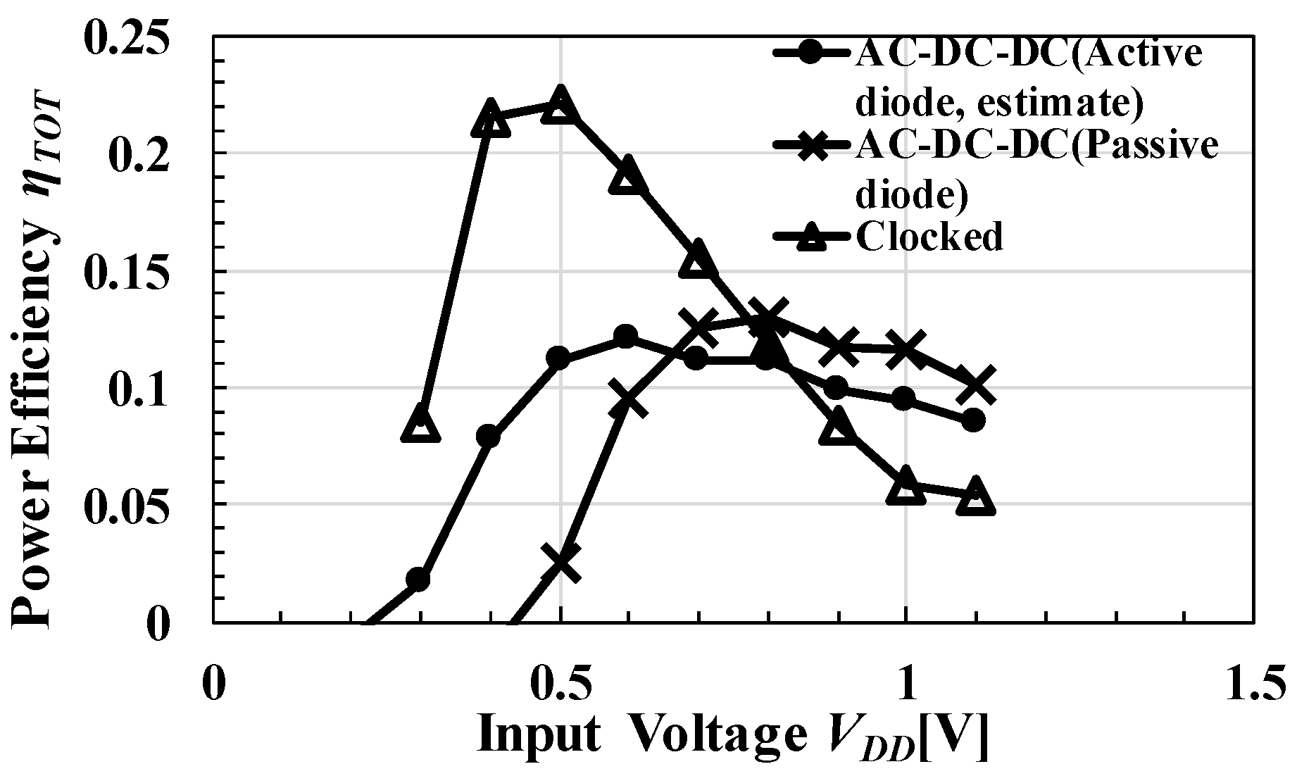
Figure 29 shows simulated ηTOT. The clocked AC-DC CP had the highest ηTOT of 22% at VDD of 0.5 V, while the AC-DC-DC CP had ηTOT of 18% at VDD of 0.8 V. The clocked AC-DC CP had a lower operation voltage than the AC-DC-DC CP did in terms of ηTOT as well as . Previous studies [9,10] have reported AC-DC conversion with active diodes that can reduce the voltage drop due to the diode threshold voltage, as shown in Figure 4b. The comparator compared the magnitude of VREC with that of VDD. When VREC became lower than VDD, PMOS was turned on with the low gate voltage and CREC was charged. Figure 28 and Figure 29 respectively show and ηTOT of the AC-DC-DC CP, which were estimated by assuming VTHD = 0 V when the active diode was used. The input power of the operational amplifier was assumed to be 1 μW. In the range of VDD ≥ 0.5 V, AC-DC-DC CP with active diodes provided higher than the proposed circuit. Because the input power of the operational amplifier was required, ηTOT became lower in the circuits with active diodes. In order to operate the operational amplifier, it is necessary to provide a power source. If VREC is used as the power source for the operational amplifier, a passive diode must be connected in parallel with the active diode for cold start. Thus, the proposed AC-DC CP can have a lower cold start voltage than AC-DC-DC CPs with a lower number of discrete components.
4.3. Comparison with Previous Researche
Table 2 shows a comparison of the proposed circuit with existing voltage boosting circuits for vibration energy harvesting in the literature.
Existence of external elements, integrated circuit area, input/output condition, power efficiency, and technology used are shown. The maximum fIN is defined by the highest frequency at which the output power is reduced by 10% from the nominal value. The proposed clocked AC-DC charge pump allows ET to operate at a frequency at least as high as 100 kHz. Due to the limitation of the measurement tool, we performed the experiment at 100 kHz or lower. Note that each paper used either ηTOT or ηSYS defined by Equations (15) and (17), respectively, for the definition of power efficiency. Compared with the previously reported circuits, the proposed circuit is only the circuit capable of obtaining an output power of an order of μW at 2 V without discrete elements. It has the smallest integrated circuit area. The authors have no appropriate way to compare power efficiency in different conditions at this point. Although the power efficiency is lower than those of the other circuits, the proposed one can be the best option when the highest priority is to generate a microwatt output power with the lowest cost and the smallest form factor. ηSYS of this work is higher than that of [10]. This could simply be because PEH of this work was smaller due to 2 × larger REH. Technology is not a significant contributor to better performance. The threshold voltage of switching transistors is critical to have a low operating voltage.
5. Future Work
In this study, only a continuous wave at a resonant frequency of the transducer was considered. Under a realistic environment, both acceleration and operating frequency vary in time. Modeling of the proposed circuit and measurement will be required to design a clocked AC-DC CP for actual use. In addition, the output voltage was not regulated internally in this work. For actual use, a control circuit must be designed to stabilize VOUT in the circuit system as shown in [23]. Furthermore, optimum design methodology needs to be established to design an optimum clocked AC-DC CP under a given condition, taking power matching at the interface between EH and CP into account. A maximum power point tracking was not considered for the clocked AC-DC CP either. It should be considered in the future.
6. Conclusions
A fully integrated clocked AC-DC charge pump circuit system was proposed, designed, and verified for vibration energy harvesting. The frequency of the clock to drive an AC-DC charge pump was upconverted with an on-chip oscillator to increase output power of the charge pump without significantly increasing the circuit area. Even with an energy transducer with REH of 500 Ω and an open circuit voltage amplitude of 0.5 V, one can obtain 4.2 μW power at 2 V with a minimal area overhead of 0.11 mm2 without using large discrete capacitors when the input frequency of 1 kHz is increased to 4.8 MHz by the on-chip oscillator. As a result, it is possible to integrate the voltage multipliers in IoT chips for vEH. In addition, the proposed circuit has negligibly small dependency of POUT on fIN. A universal design can be applied to various energy transducers with different resonant frequencies. The fabricated clocked AC-DC CP was measured with a magnetostrictive transducer. POUT of 2 μW–30 μW was obtained with α of 0.2 G to 0.7 G at VOUT of 2 V. Compared with the previously reported circuits, the proposed circuit is only the circuit capable of obtaining an output power of a microwatt order at 2 V without discrete elements.
Author Contributions
Conceptualization, T.T.; methodology, H.K. and T.T.; software, H.K.; validation, H.K. and T.T.; formal analysis, H.K. and T.T.; investigation, H.K. and T.T.; writing—original draft preparation, H.K.; writing—review and editing, T.T.; funding acquisition, T.T. All authors have read and agreed to the published version of the manuscript.
Funding
This research was partially funded by Micron Foundation.
Acknowledgments
This work was supported by VDEC; Synopsys, Inc.; Cadence Design Systems, Inc.; Rohm Corp.; and Micron Foundation. The authors wish to thank T. Ueno for sharing a magnetostrictive transducer for our experiments and M. Futagawa, H. Hirano, and S. Ota for technical discussion.
Conflicts of Interest
The authors declare no conflict of interest.
Nomenclature
| C | Capacitance per stage | POUT | Output power of the charge pump |
| fCLK | Frequency of a clock generated by ring oscillator | PRE | Reactive power |
| fIN | Frequency of harvester’s output power | PTOT | Power of the system |
| Input current of the charge pump | REH | Output impedance of energy harvester | |
| IOSC | Current driving the oscillator | RTOT | Total output impedance of the system |
| Output current of the charge pump | VDD | AC input voltage amplitude | |
| IS | Diode saturation current | VOUT | Output voltage of the charge pump |
| N | Stage number of the charge pump | VREC | Rectified voltage |
| PCP | Input power of the charge pump | VSS | Ground |
| PEH | Power generated by energy harvesting | VTHEFF | Effective threshold voltage of diode |
| PLOSS | Power loss in the charge pump | VT | Thermal voltage |
| POSC | Power of the oscillator | β | Ratio of parasitic capacitance to C |
| CINV | Load capacitance of the oscillator | θS | Phase at which the output current begins to flow |
| α | Vibration acceleration |
References
- Mitcheson, P.D.; Rao, G.K.; Green, T.C. Energy Harvesting from Human and Machine Motion for Wireless Electronic Devices. Proc. IEEE 2008, 96, 1457–1486. [Google Scholar] [CrossRef] [Green Version]
- Manoli, Y. Energy harvesting from devices to systems. In Proceedings of the 2010 Proceedings of ESSCIRC, Institute of Electrical and Electronics Engineers (IEEE), Seville, Spain, 14–16 September 2010; pp. 27–36. [Google Scholar]
- Chao, L.; Tsui, C.-Y.; Ki, W.-H. A Batteryless Vibration-based Energy Harvesting System for Ultra Low Power Ubiquitous Applications. In Proceedings of the 2007 IEEE International Symposium on Circuits and Systems, Institute of Electrical and Electronics Engineers (IEEE), New Orleans, LA, USA, 27–30 May 2007; pp. 1349–1352. [Google Scholar]
- Arakawa, Y.; Suzuki, Y.; Kasagi, N. Micro Seismic Power Generator Using Electret Polymer Film. Proc. Natl. Symp. Power Energy Syst. 2004, 2005, 37–38. [Google Scholar] [CrossRef]
- Ueno, T. Magnetostrictive vibrational power generator for battery-free IoT application. AIP Adv. 2019, 9, 35018. [Google Scholar] [CrossRef] [Green Version]
- Stanzlone, S.; Liempd, C.; Schaijk, R. A Self-Biased 5-to-60V Input Voltage and 25-to- 1600μW Integrated DC-DC Buck Converter with Fully Analog MPPT Algorithm Reaching up to 88% End-to-End Efficiency. IEEE Int. Solid-State Circuits Conf. 2013, 2, 74–76. [Google Scholar]
- Tom, J.; Kaźmiersuki, S.B. Energy Harvesting Systems: Principles, Modeling and Applications; Springer: Berlin/Heidelberg, Germany, 2010; Chapter 1. [Google Scholar]
- Rahimi, A.; Zorlu, O.; Külah, H.; Muhtaroglu, A. An interface circuit prototype for a vibration-based electromagnetic energy harvester. In Proceedings of the 2010 International Conference on Energy Aware Computing, Institute of Electrical and Electronics Engineers (IEEE), Cairo, Egypt, 16–18 December 2010; pp. 1–4. [Google Scholar]
- Maurath, D.; Becker, P.F.; Spreemann, D.; Manoli, Y. Efficient Energy Harvesting with Electromagnetic Energy Transducers Using Active Low-Voltage Rectification and Maximum Power Point Tracking. IEEE J. Solid-State Circuits 2012, 47, 1369–1380. [Google Scholar] [CrossRef]
- Ulusan, H.; Gharehbaghi, K.; Zorlu, O.; Muhtaroglu, A.; Külah, H. A Fully Integrated and Battery-Free Interface for Low-Voltage Electromagnetic Energy Harvesters. IEEE Trans. Power Electron. 2014, 30, 3712–3719. [Google Scholar] [CrossRef]
- Wang, S.-W.; Ke, Y.-W.; Huang, P.-C.; Hsieh, P.-H. Electromagnetic Energy Harvester Interface Design for Wearable Applications. IEEE Trans. Circuits Syst. II Express Briefs 2018, 65, 667–671. [Google Scholar] [CrossRef]
- Karthaus, U.; Fischer, M. Fully integrated passive uhf rfid transponder ic with 16.7-μ minimum rf input power. IEEE J. Solid-State Circuits 2003, 38, 1602–1608. [Google Scholar] [CrossRef]
- Papotto, G.; Carrara, F.; Palmisano, G. A 90-nm CMOS Threshold-Compensated RF Energy Harvester. IEEE J. Solid-State Circuits 2011, 46, 1985–1997. [Google Scholar] [CrossRef]
- Kawauchi, H.; Tanzawa, T. A clocked AC-DC voltage multiplier for increasing the power conversion efficiency in vibration energy harvesting. In Proceedings of the IEICE General Conference, Tokyo, Japan, 20–23 March 2018; Available online: http://hdl.handle.net/10297/00025812 (accessed on 20 March 2018).
- Kawauchi, H.; Tanzawa, T. A 2V 3.8 µW Fully-Integrated Clocked AC-DC Charge Pump with 0.5 V 500 Ω Vibration Energy Harvester. In Proceedings of the IEEE Asia Pacific Conference on Circuits and Systems, Bangkok, Thailand, 11–14 November 2019; pp. 329–332. [Google Scholar]
- Tanzawa, T. An Analytical Model of Charge Pump DC-DC Voltage Multiplier Using Diodes. IEICE Trans. Fundam. Electron. Commun. Comput. Sci. 2017, 1137–1144. [Google Scholar] [CrossRef]
- Tanzawa, T. Design of DC-DC Switched-Capacitor Voltage Multiplier driven by DC Energy Harvester. In Proceedings of the IEEE International Conference on Electronics Circuits and Systems, Marseille, France, 7–10 December 2014; pp. 327–330. [Google Scholar]
- Tanzawa, T. An Optimum Design for Integrated Switched-Capacitor Dickson Charge Pump Multipliers with Area Power Balance. IEEE Trans. Power Electron. 2014, 29, 534–538. [Google Scholar] [CrossRef]
- Peters, C.; Kessling, O.; Henrici, F.; Ortmanns, M.; Manoli, Y. CMOS Integrated Highly Efficient Full Wave Rectifier. IEEE Int. Symp. Circuits Syst. 2007, 2415–2418. [Google Scholar] [CrossRef]
- Haddad, P.; Gosset, G.; Raskin, J.; Flandre, D. Automated Design of a 13.56 MHz 19 μW Passive Rectifier with 72% Efficiency Under 10 μA load. IEEE J. Solid-State Circuits 2016, 51, 5. [Google Scholar] [CrossRef]
- Tokuda, S.; Tanzawa, T. Toward a Minimum-Operating-Voltage Design of DC-DC Charge Pump Circuits for Energy Harvesting. IEEE Int. Symp. Circuits Syst. (ISCAS) 2019, 1–4. [Google Scholar] [CrossRef]
- Leicht, J. CMOS Circuits for Electromagnetic Vibration Energy Harvesters: System Modeling, Interface Design and Implementation. Ph.D. Thesis, University of Freiburg, Fahnenbergplatz, Germany, July 2019. Chapter 2. [Google Scholar] [CrossRef]
- Tanzawa, T. A Behavior Model of an On-Chip High Voltage Generator for Fast, System-Level Simulation. IEEE Trans. Very Large Scale Integr. (VLSI) Syst. 2011, 20, 2351–2355. [Google Scholar] [CrossRef]
Figure 1.
AC-DC charge pump (CP) [8].
Figure 1.
AC-DC charge pump (CP) [8].
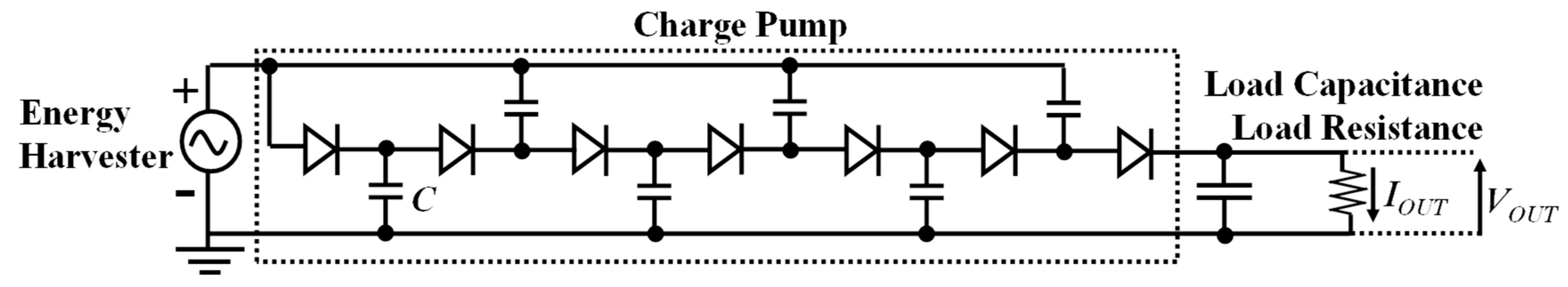
Figure 2.
Simulated POUT as a function of C (AC-DC CP, VDD = 0.5 V, VOUT = 2 V, N = 9, fIN = 1 kHz).
Figure 2.
Simulated POUT as a function of C (AC-DC CP, VDD = 0.5 V, VOUT = 2 V, N = 9, fIN = 1 kHz).
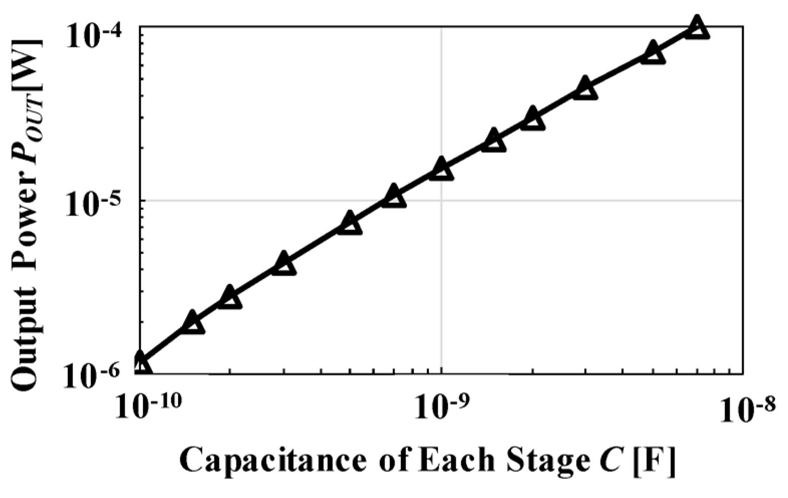
Figure 3.
AC-DC-DC CP (FBR: full bridge rectifier, OSC: oscillator).
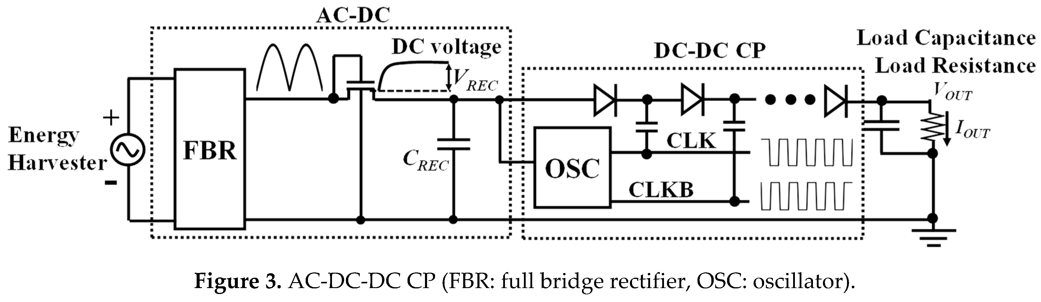
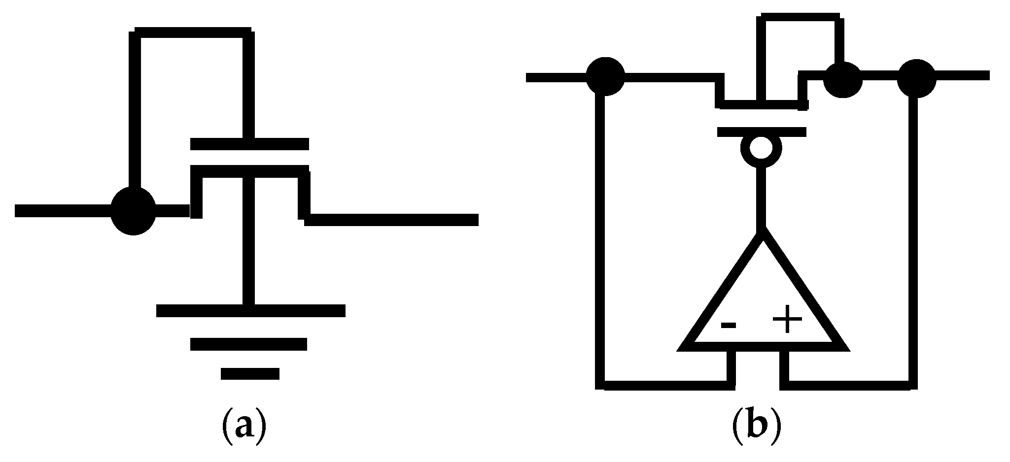
Figure 5.
Clocked AC-DC CP.
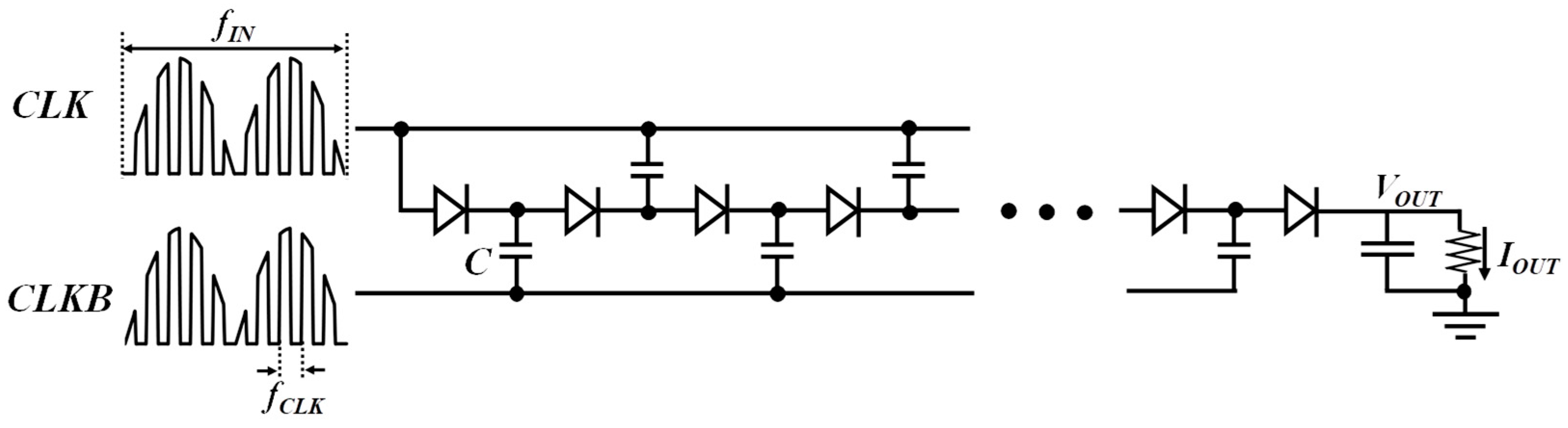
Figure 6.
Waveform of the clocked AC-DC CP: (a) VREC, (b) CLK, (c) IOUT.
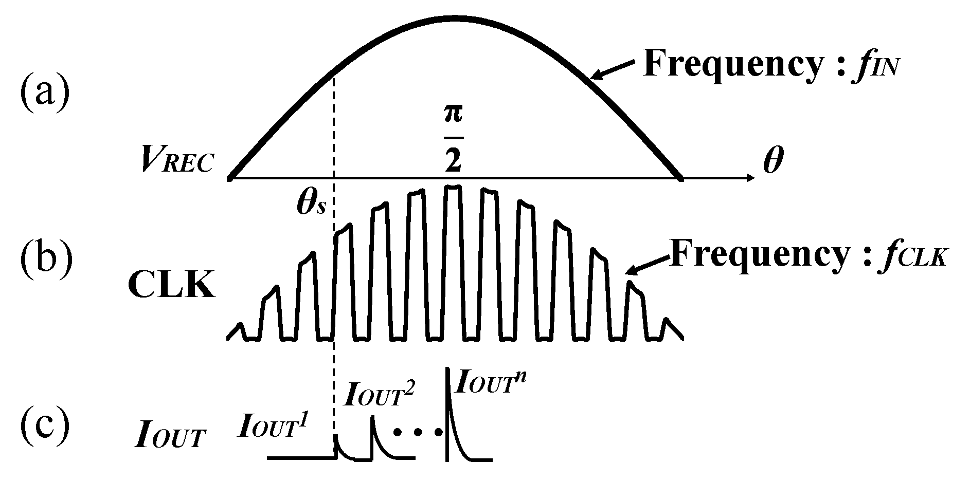
Figure 7.
Equivalent circuit for the system including AC energy transducer and CP based on [15] for DC energy transducer. (a) can be transformed into (b).
Figure 7.
Equivalent circuit for the system including AC energy transducer and CP based on [15] for DC energy transducer. (a) can be transformed into (b).
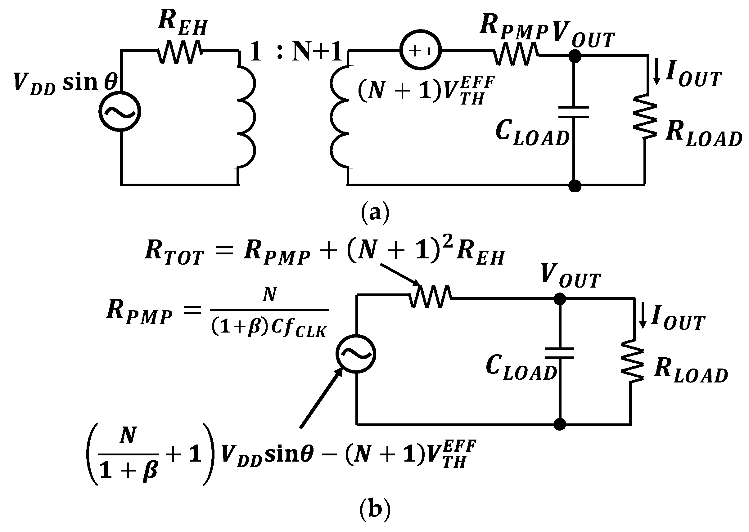
Figure 8.
System diagram of the clocked AC-DC CP.
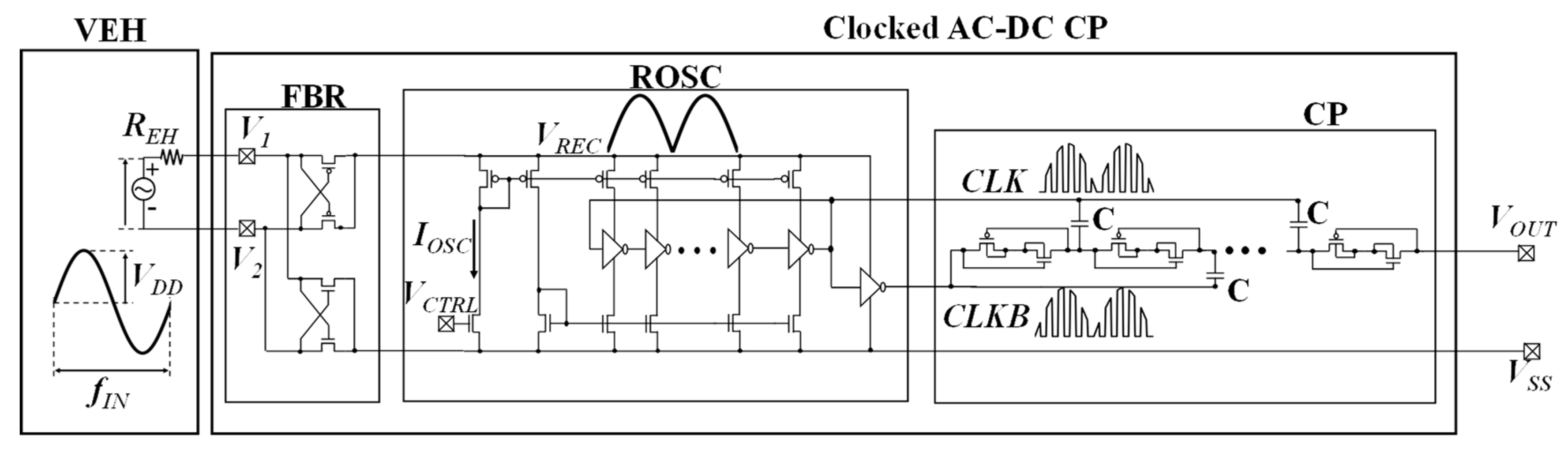
Figure 9.
Measurement circuit.
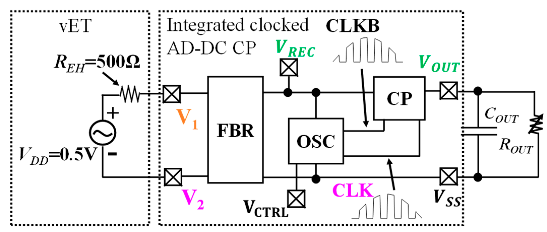
Figure 10.
Die photo of the proposed system.
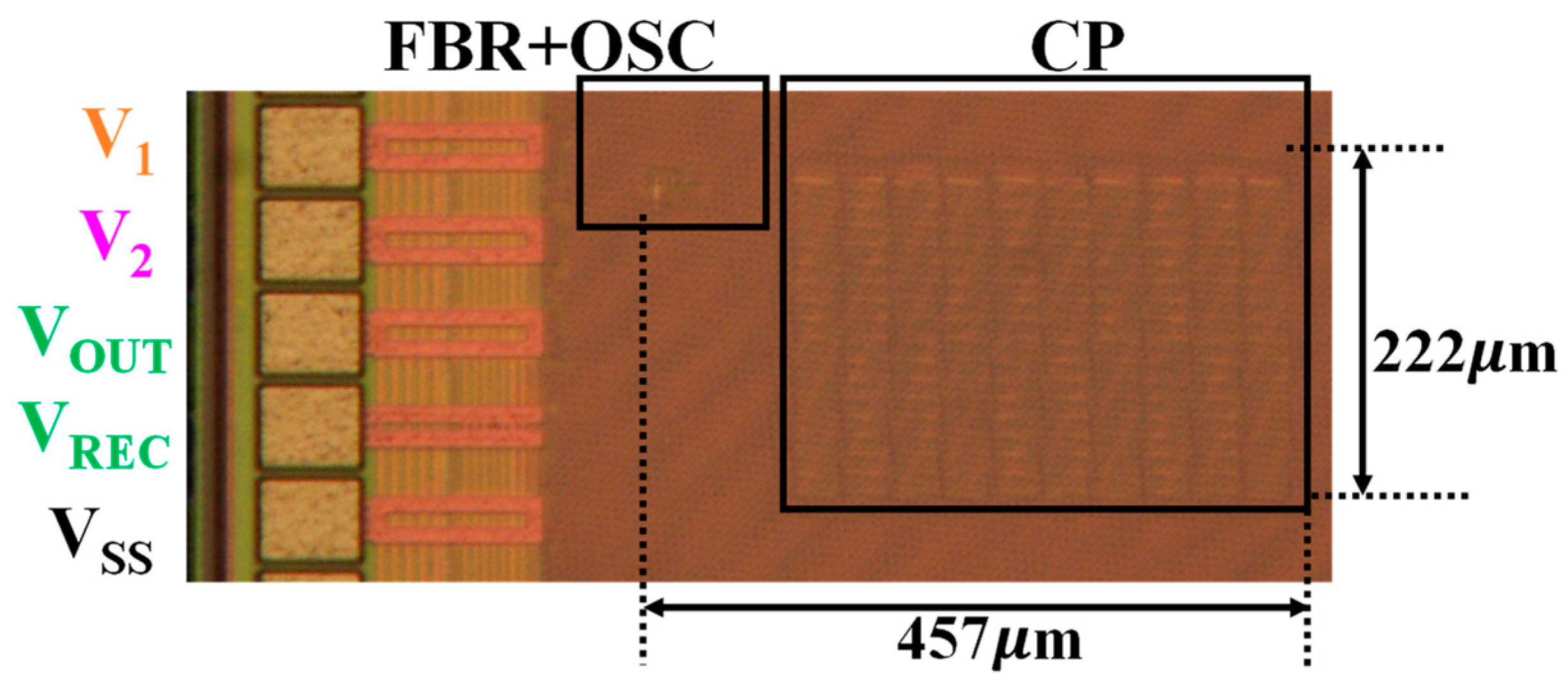
Figure 11.
Measured waveforms (a) V1–V2, VREC and CLK, (b) CLK and VREC, (c) V1−V2 and VOUT.

Figure 12.
as a function of fCLK (VDD = 0.5 V, VOUT = 2 V, fIN = 1 kHz).
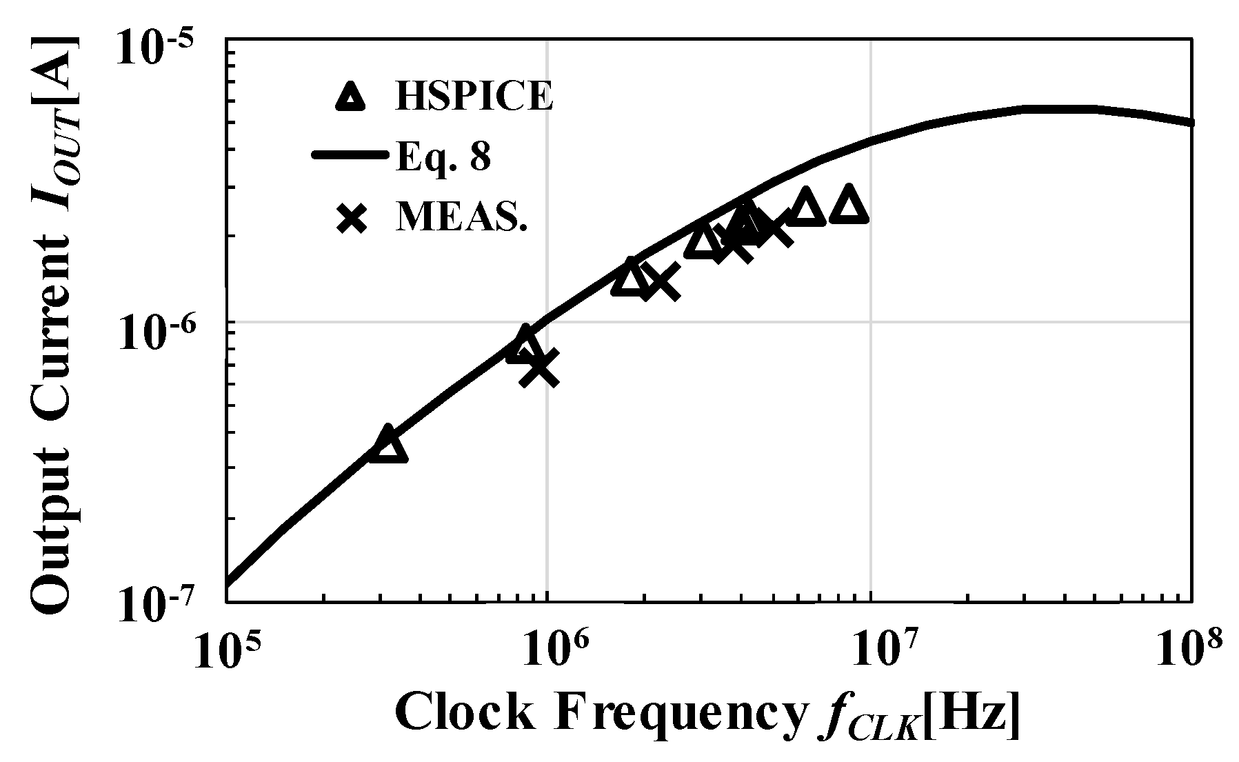
Figure 13.
PTOT as a function of fCLK (VDD = 0.5 V, VOUT = 2 V, fIN = 1 kHz).
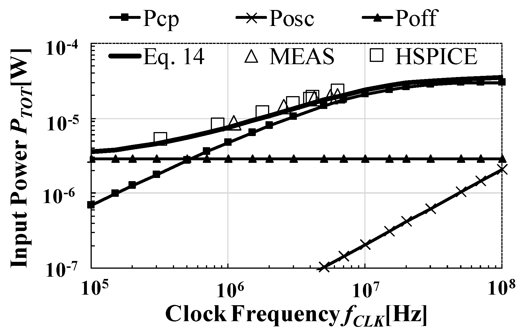
Figure 14.
ηTOT as a function of fCLK (VDD = 0.5 V, VOUT = 2 V, fIN = 1 kHz).
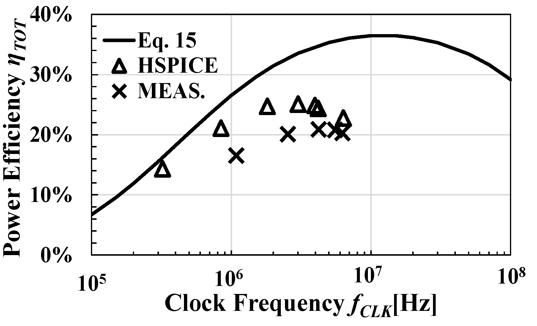
Figure 15.
Measured as a function of VOUT (fIN = 1 kHz, fCLK = 5 MHz).
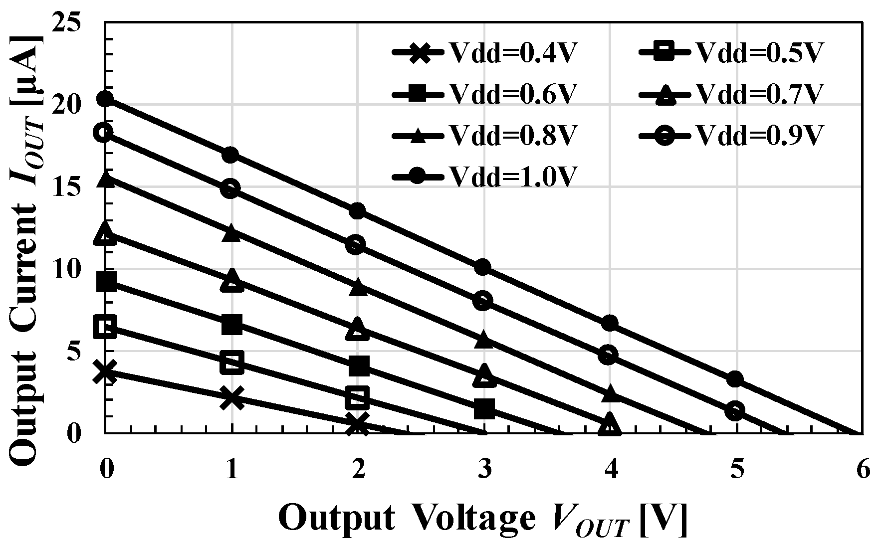
Figure 16.
(a)–VDD, (b) ηSYS–PEH (fIN = 1 kHz, fCLK = 5 MHz, VOUT = 2 V).

Figure 17.
Measured IOUT as a function of fIN (VDD = 0.5 V, VOUT = 2 V, fCLK = 5 MHz).
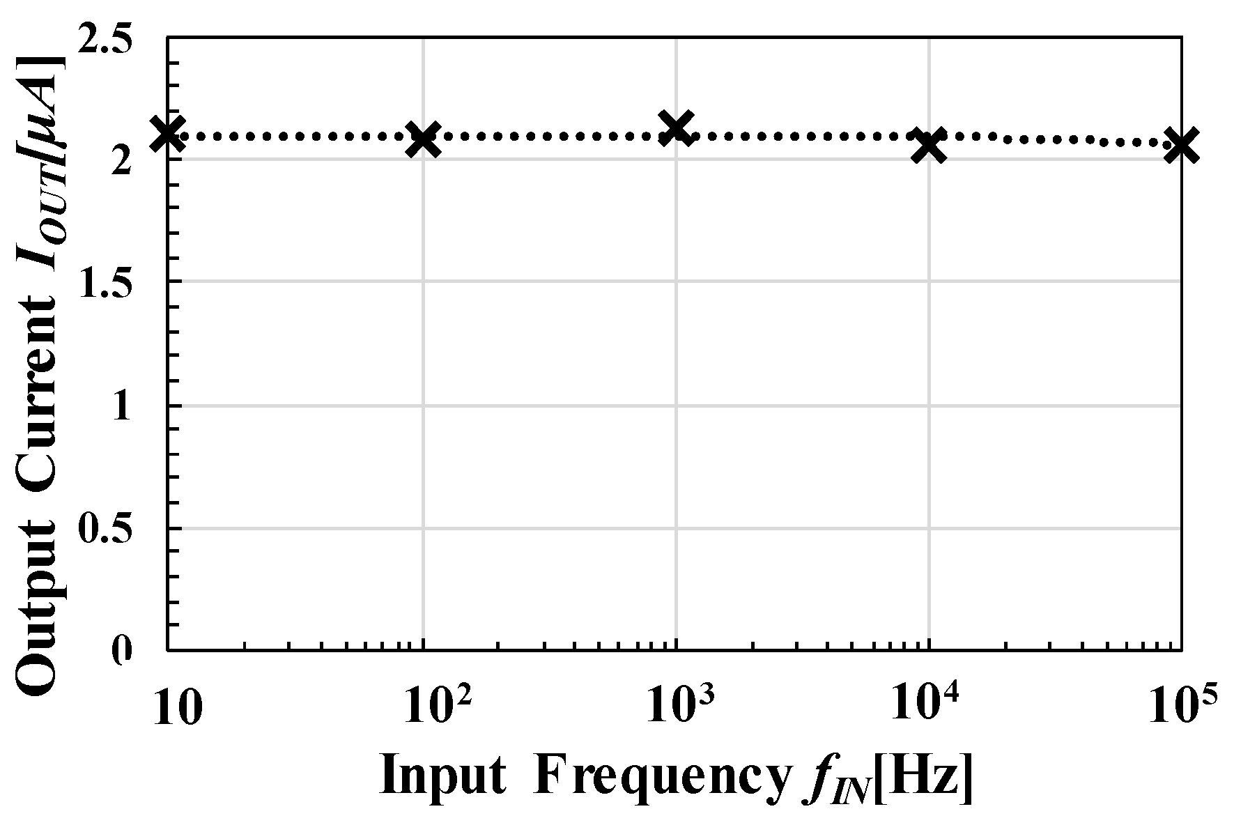
Figure 18.
Measurement set-up: photograph (a) and block diagram (b).

Figure 19.
Measured VDD as a function of α (RL = ∞, α = 0.5 G).
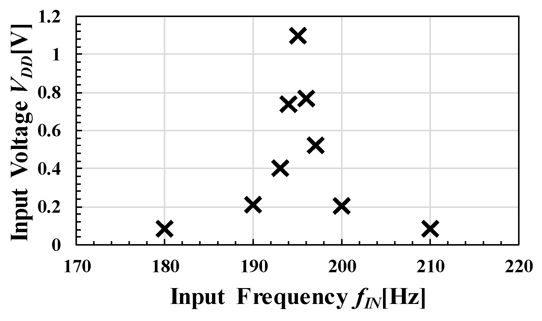
Figure 20.
Measured VDD as a function of α (RL = ∞, fIN = 195 Hz).

Figure 21.
Output voltage of power generating element (fIN = 195 Hz): (a) α = 0.28 G, (b) α = 0.5 G.
Figure 21.
Output voltage of power generating element (fIN = 195 Hz): (a) α = 0.28 G, (b) α = 0.5 G.
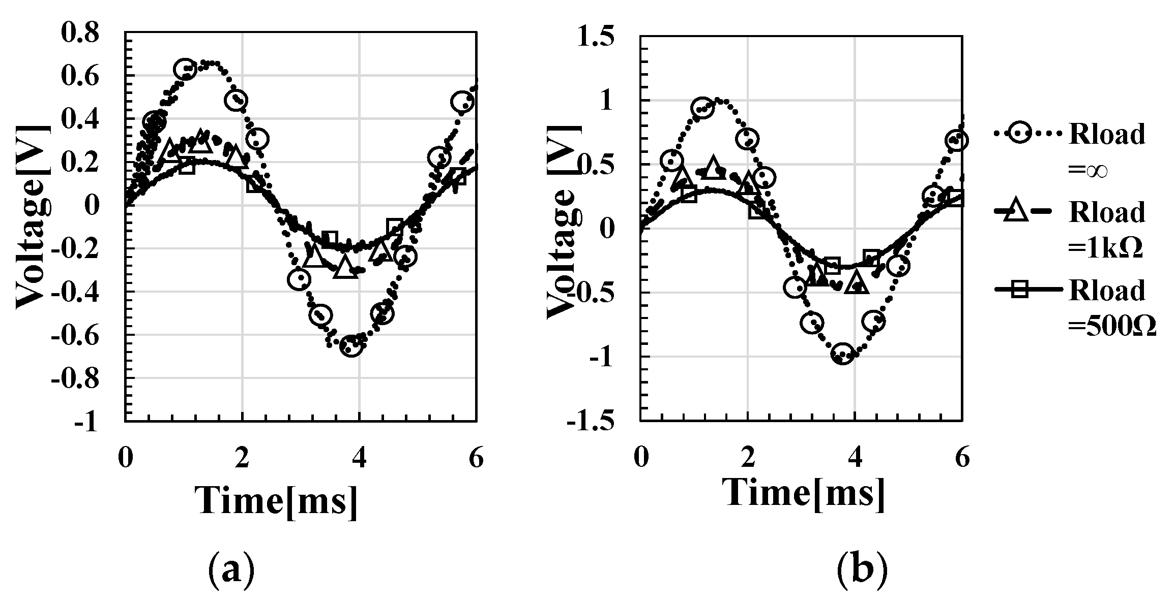
Figure 22.
as a function of fCLK (VOUT = 2 V, fIN = 195 Hz): (a) α = 2.7 m/s2, (b) α = 4.9 m/s2.
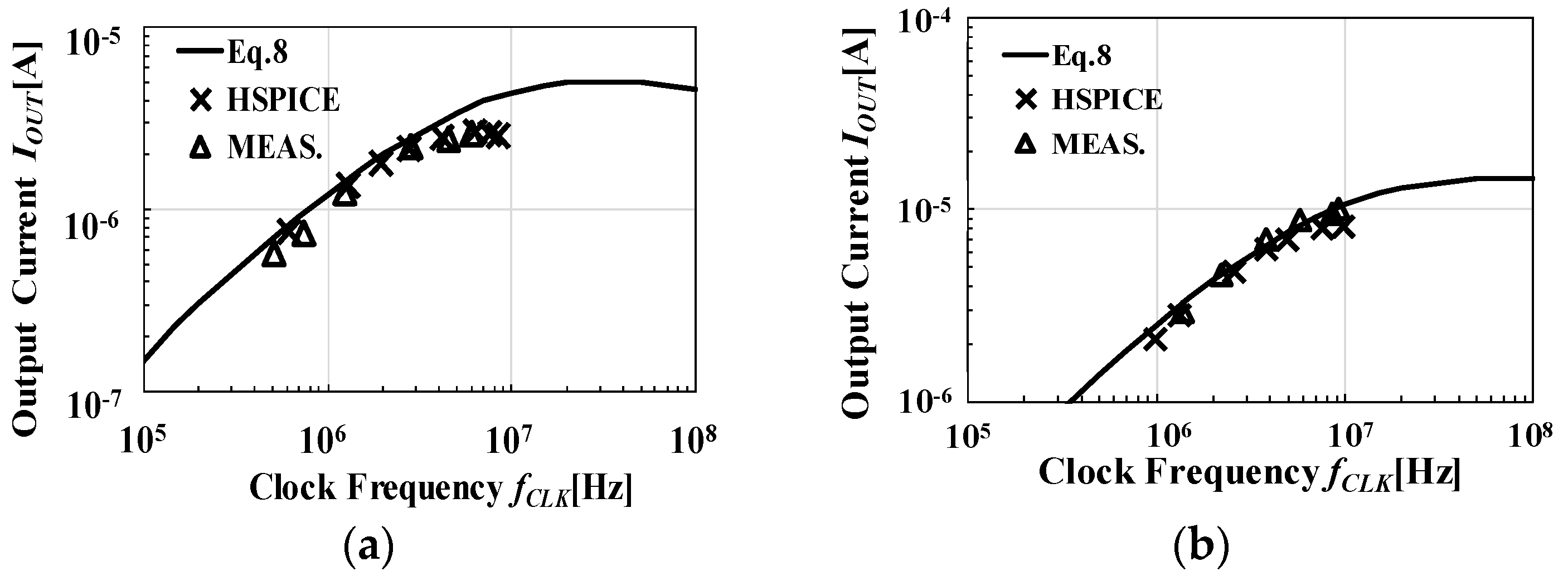
Figure 23.
Measured VDD as a function of α (VOUT = 2 V, fIN = 195 Hz, fCLK = 5 MHz).

Figure 24.
Measured as a function of α (VOUT = 2 V, fIN = 195 Hz, fCLK = 5 MHz).
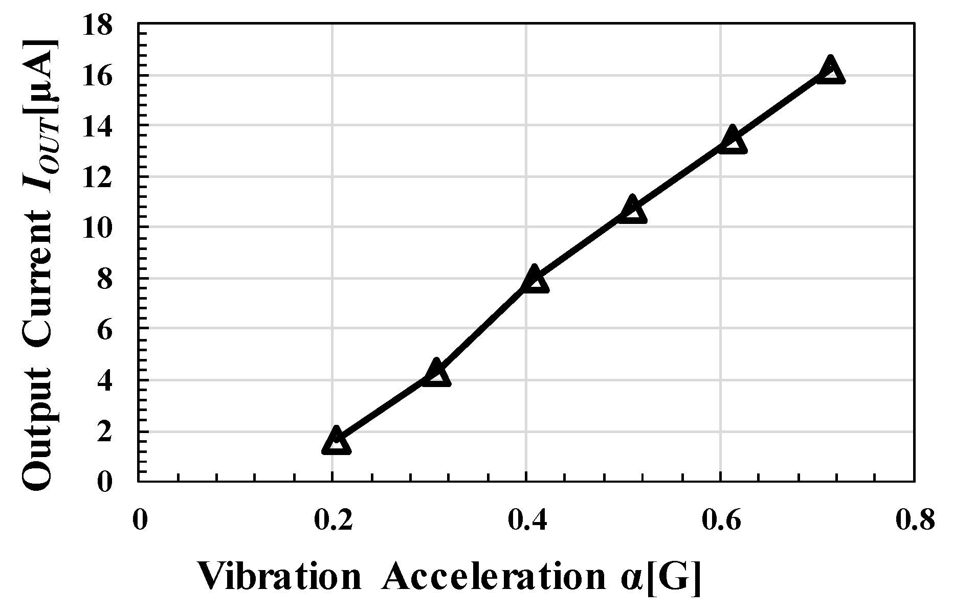
Figure 25.
as a function of VOUT (AC-DC CP, fIN = 1 kHz, VDD = 0.5 V, REH = 500 Ω).
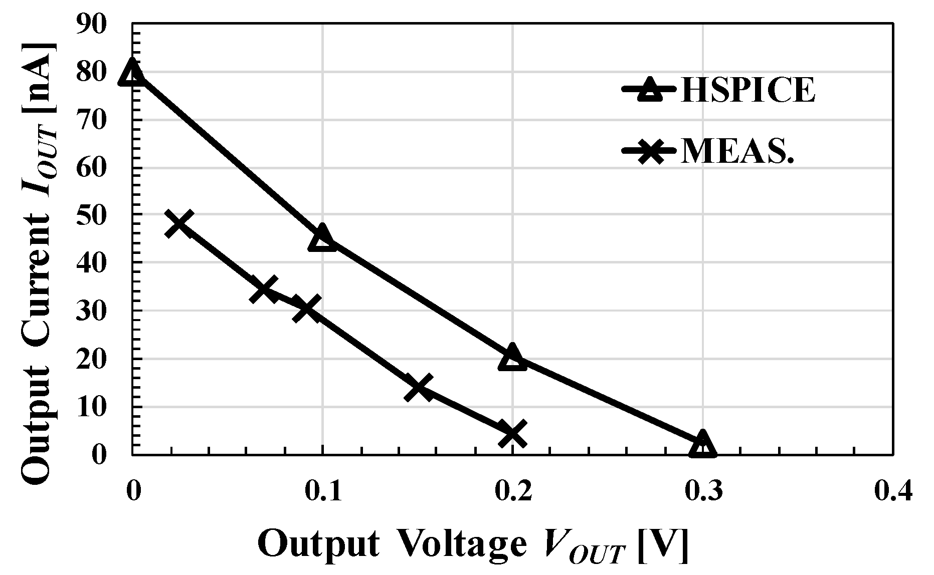
Figure 26.
Comparison of power distribution.
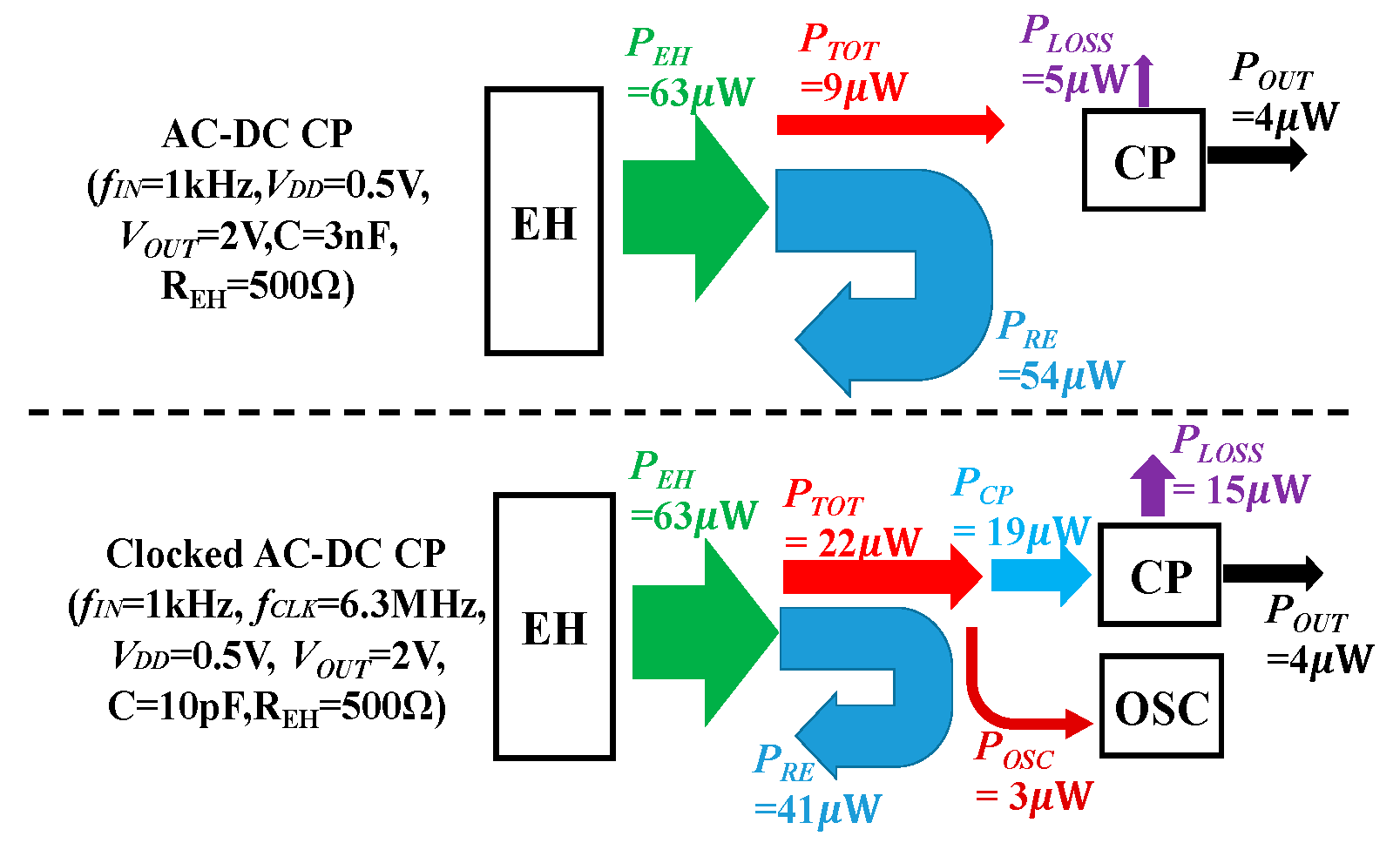
Figure 27.
Simulated as a function of VOUT (fIN = 1 kHz, fCLK = 1 MHz, VDD = 0.5 V, REH = 500 Ω).

Figure 28.
Simulated as a function of VDD (fIN = 1 kHz, fCLK = 1 MHz, VDD = 0.5 V, REH = 500 Ω).
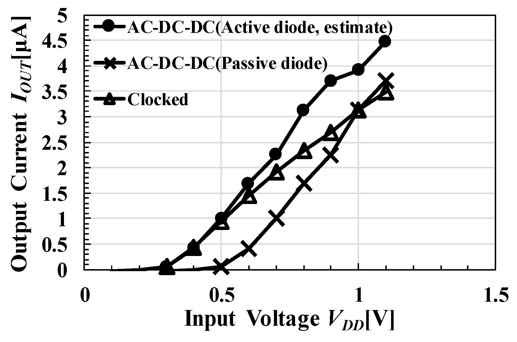
Figure 29.
Simulated ηTOT as a function of VDD (fIN = 1 kHz, fCLK = 1 MHz, VDD = 0.5 V, REH = 500 Ω).
Figure 29.
Simulated ηTOT as a function of VDD (fIN = 1 kHz, fCLK = 1 MHz, VDD = 0.5 V, REH = 500 Ω).

Table 1.
Characteristics of vibration energy transducer.
| Piezoelectric [3] | Electrostatic [4] | Magnetostrictive [5] | |
|---|---|---|---|
| Nominal output impedance | 100 kΩ–1 MΩ | 100 MΩ–1 GΩ | 100 Ω–1 kΩ |
| Nominal output voltage | 1 V–10 V | 10 V–100 V | 0.1 V–1 V |
| Output power (mW/cm3) | 0.74–3 [7] | 0.08–0.6 [7] | 20 [5] |
Table 2.
Comparison on the characteristics.
| ET * | Boosting Method | Discrete Element (Values) * | Circuit Area | Maximum fIN | Power Efficiency | CMOS | ||||
|---|---|---|---|---|---|---|---|---|---|---|
| VDD | VOUT | POUT | REH | |||||||
| [8] | EM | AC-DC CP | 3C + 4D (N.A.) | Discrete | N.A. | 25% (ηTOT) | - | |||
| N.A. | 2 V | 30 μW | N.A. | |||||||
| [9] | EM | AC-DC-DC CP | 1C (10 nF) | 0.58 mm2 + 4.84 mm2 | 10 kHz (Est.) | 37% (ηSYS) | 0.35 μm | |||
| 1.2 V | 2 V | 33 μW | 2k Ω | |||||||
| [10] | EM | AC-DC-DC CP | 1C (1 μF) | N.A. | 30kHz | 13% (ηTOT) | 90 nm | |||
| 0.5 V | 1.8 V | 3.2 μW | 180 Ω | |||||||
| [11] | EM | Rectifier + switching regulator | 1L (N.A.) | 1.6 × 1.6 mm2 | N.A. | 67% (ηSYS) | 0.18 μm | |||
| 0.6 V | 1 V | 1 mW | 120 Ω | |||||||
| This work | MS | Clocked AC-DC CP | None | 0.11 mm2 | 100 kHz or higher | 23% (ηTOT), 6% (ηSYS) | 65 nm | |||
| 0.5 V | 2 V | 4.2 μW | 500 Ω | |||||||
* ET: energy transducer, EM: electromagnetic, MS: magnetostrictive, C: chip capacitor, D: chip diode, L: chip inductor.
Publisher’s Note: MDPI stays neutral with regard to jurisdictional claims in published maps and institutional affiliations. |
© 2020 by the authors. Licensee MDPI, Basel, Switzerland. This article is an open access article distributed under the terms and conditions of the Creative Commons Attribution (CC BY) license (http://creativecommons.org/licenses/by/4.0/).
Share and Cite
MDPI and ACS Style
Kawauchi, H.; Tanzawa, T. A Fully Integrated Clocked AC-DC Charge Pump for Mignetostrictive Vibration Energy Harvesting. Electronics 2020, 9, 2194. https://doi.org/10.3390/electronics9122194
AMA Style
Kawauchi H, Tanzawa T. A Fully Integrated Clocked AC-DC Charge Pump for Mignetostrictive Vibration Energy Harvesting. Electronics. 2020; 9(12):2194. https://doi.org/10.3390/electronics9122194
Chicago/Turabian StyleKawauchi, Hayato, and Toru Tanzawa. 2020. "A Fully Integrated Clocked AC-DC Charge Pump for Mignetostrictive Vibration Energy Harvesting" Electronics 9, no. 12: 2194. https://doi.org/10.3390/electronics9122194
Note that from the first issue of 2016, this journal uses article numbers instead of page numbers. See further details here.