1. Introduction
Modern telecommunication systems, such as full-duplex architectures, are increasingly evolving toward integrated designs that combine both transmit (Tx) and receive (Rx) functionalities within compact terminals. In these configurations, certain components—particularly the phase shifter in a phased array antenna—are often shared between the Tx and Rx signal paths [
1,
2,
3]. However, a significant challenge in such integration is the leakage of nonlinear distortion generated by the phase shifter into the Rx path when high-power Tx signals pass through it. Since the Tx and Rx frequencies are typically closely spaced, this distortion can fall within the receiver’s operating band and interfere with the desired signal, thereby degrading receiver sensitivity and overall system performance. While the design in this work targets the 2 GHz band to address the stringent linearity demands of 4G cellular network phased arrays, the concepts are broadly applicable to other phased array systems such as radar and satellite communications, with appropriate frequency scaling.
A digital phase shifter typically consists of two main parts: switch part and phase-shifting section [
3,
4,
5,
6,
7,
8,
9]. Among these, the switching part often imposes a limitation on the overall linearity of the phase shifter. Various RF switch technologies have been explored in the literature to address this challenge, including micro-electromechanical systems (MEMS) [
10], phase change materials [
11], plasma [
12], graphene flakes [
13], and Field-Effect Transistors (FETs) [
14,
15,
16,
17,
18]. Despite these alternatives, PIN diodes [
2,
3,
9,
19,
20] have demonstrated superior linearity performance, along with reasonably fast switching speeds and high power-handling capability, making them a preferred choice for many high-performance applications.
Previous studies have proposed various techniques to enhance the linearity of PIN diode-based RF switches, which are commonly used in switched-line phase shifters. In [
3,
19,
21], the impact of impedance on the linearity of these switches was analyzed, demonstrating that reducing the impedance seen by the PIN diode can significantly improve its linearity performance. Applying this technique to a 3-bit switched-line phase shifter resulted in an IIP3 of 90 dBm. In another line of work [
2,
9], the linearity of different switch topologies using PIN diodes was explored. These studies showed that incorporating a quarter-wavelength transmission line between two PIN diodes in a hybrid configuration can enhance the linearity of the switch, achieving an IIP3 of up to 95 dBm.
In this paper, a novel design for a highly linear digital phase shifter is proposed, combining coupler-based impedance transformers and loaded-line phase shifters. The proposed architecture is both simulated and fabricated to validate its effectiveness. The measured results demonstrate an IIP3 of 100 dBm under a 25 W (44 dBm) input power condition.
Section 2 of this paper provides a brief discussion on the distortion characteristics of PIN diodes, as well as the influence of impedance and circuit topology on linearity.
Section 3 details the loaded-line phase shifter configuration and the implementation of the proposed design. Measurement results and a performance comparison table are presented in
Section 4.
2. Distortion in PIN Diodes
PIN diodes introduce distortion in both their ON and OFF states, with noticeably worse linearity in the OFF state. Particular emphasis is placed on improving the OFF-state linearity of the PIN diodes, which typically governs the overall IIP3 performance due to their inherently lower linearity [
3,
22,
23,
24,
25,
26,
27,
28]. Digital phase shifters employing PIN diodes as switching elements can be implemented using various topologies, including switched-line, reflective, and loaded-line techniques. Phase shifting is achieved by toggling the states of the PIN diodes. Several studies have examined the factors affecting the linearity of PIN diode-based RF switches. In [
2,
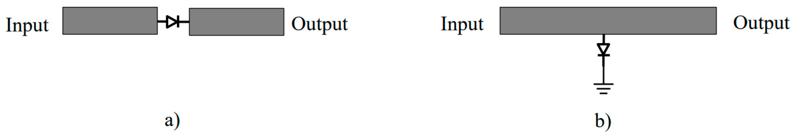
9], it was demonstrated that the switch topology—illustrated in
Figure 1—is a critical factor influencing linearity performance. It is worth noting that in the parallel topology (
Figure 1b), the OFF state is achieved by turning the PIN diode ON, thereby presenting a low-impedance shunt path to ground that reflects the incoming signal, effectively blocking transmission to the output. The comparative analysis in [
2,
9] showed that in the parallel topology, the IIP3 in the OFF state was significantly higher than in the series topology, indicating better linearity. However, the main drawback of the parallel topology is its poor isolation, as it does not effectively block signals in the OFF state. This limitation makes it less suitable for applications requiring high isolation. Nonetheless, in a loaded-line phase shifter, the switching element does not need to fully block the signal. Instead, it is used to connect or disconnect an impedance element from the main transmission line. Therefore, the parallel topology becomes a practical choice for loaded-line architectures, where the switch only needs to insert or remove a segment without affecting signal loss, while still enabling the desired phase shift.
In [
3,
19,
21], the impact of the impedance seen by the PIN diode on its linearity was examined in detail. The studies revealed that the IIP3 in the ON state increases with higher impedance, whereas the IIP3 in the OFF state decreases. Conversely, lowering the impedance leads to a reduction in IIP3 (ON) but an improvement in IIP3 (OFF). Although 50 Ω is commonly used as the characteristic impedance (
), these findings suggest a potential strategy for enhancing the linearity of PIN diodes in the OFF state by deliberately reducing the impedance they see. By doing so, the IIP3 (OFF)—often the limiting factor in overall phase shifter linearity—can be significantly improved, even if it comes at the expense of a slightly lower IIP3 (ON). This trade-off ultimately benefits the total linearity performance of the phase shifter [
3,
19,
21]. This impedance optimization inevitably involves a trade-off: reducing the impedance improves the OFF-state IIP3 by minimizing voltage swings, while slightly reducing ON-state IIP3 by limiting RF current. Since the ON-state linearity is intrinsically better, this trade-off is acceptable and ensures the overall phase shifter performance is governed by an improved, higher OFF-state IIP3, as detailed in [
3,
19].
The combination of a parallel-loaded-line phase shifter with a coupler-based impedance transformer directly mitigates nonlinear distortion leakage—a key challenge in shared Tx/Rx phased array systems—by reducing voltage swings across the PIN diodes.
3. Loaded-Line Phase Shifter
The fundamentals and various implementations of loaded-line phase shifters are discussed in detail in [
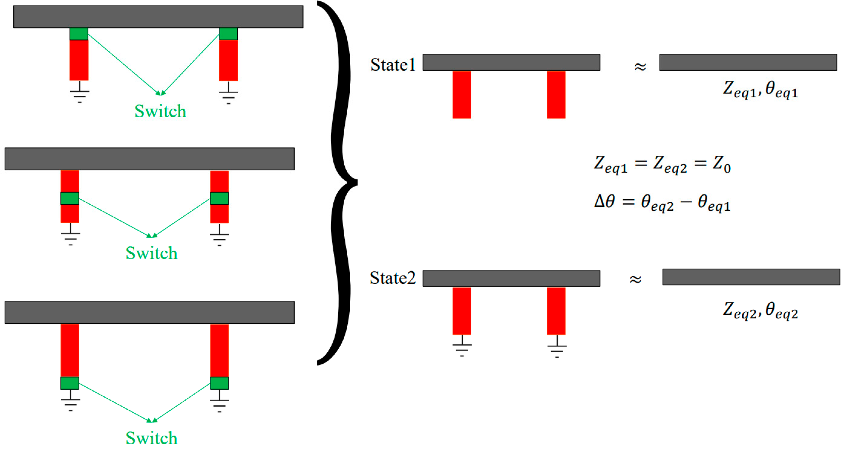
26]. In this type of phase shifter, the desired phase shift is achieved by selectively controlling stubs or lumped elements connected to the main transmission line. Regardless of the specific implementation, the core concept for achieving a target phase shift,
, is illustrated in
Figure 2. In each switching state, the phase shifter can be modeled as an equivalent transmission line with a characteristic impedance of
and length of
. To achieve a well-matched and effective phase shift, the design must ensure that
, and that the differential phase shift satisfies
.
In addition to the dimensions of the stubs—such as their width, length, and position relative to the main line—the parasitic parameters of the switching elements also play a critical role in determining the resulting phase shift and insertion loss (IL). These effects must be carefully accounted for during the design process. A comprehensive mathematical framework for calculating the required stub dimensions to achieve a specified phase shift is provided in [
26,
29].
Although the loaded-line phase shifter offers linearity advantages by utilizing PIN diodes in a parallel configuration, its maximum achievable IIP3 can be even better by using impedance transformer. As reported in [
8], an RF switch employing the BAR64-02V PIN diode in a parallel configuration demonstrated an IIP3 of approximately 90 dBm at 2.05 GHz.
To further enhance the IIP3, the impedance optimization technique presented in [
3] can be employed. This approach suggests that connecting the PIN diode to a lower impedance improves the overall IIP3 of the switch including the IIP3 (ON) and IIP3 (OFF). Our measurement results, shown in
Figure 3, support this observation. In these experiments, a BAR64-02V PIN diode configured in a series topology was evaluated under varying impedance conditions. The results confirm that both ON- and OFF-state linearity are strongly influenced by the impedance seen by the diode. This finding reinforces the effectiveness of impedance transformation in enhancing the overall linearity performance of PIN diode-based switches.
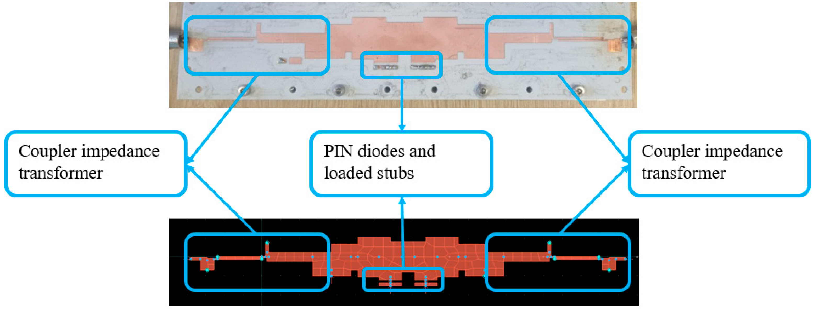
To adjust the impedance seen by the PIN diodes, impedance transformers are incorporated on both sides of the loaded-line phase shifter. The coupler-based impedance transformers at the input and output serve to present a reduced impedance to the PIN diodes—thereby improving linearity—while simultaneously matching the overall phase shifter to standard 50 Ω ports. This dual transformation ensures both optimal PIN diode operation and seamless integration into typical RF systems. The structure of the proposed highly linear loaded-line phase shifter is illustrated in
Figure 4. In this configuration, each switching element consists of a single PIN diode connected in a parallel-to-ground arrangement. Despite the addition of impedance transformers, the input and output impedance of the overall phase shifter is maintained at 50 Ω to ensure compatibility with standard RF systems. The reduced impedance presented by the coupler minimizes voltage swings across the reverse-biased diodes, thereby directly enhancing the OFF-state IIP3, as validated by our measurements and analyses in [
3,
19].
4. Measurement Results and Discussion
To demonstrate the effectiveness of the proposed concept, a one-bit loaded-line phase shifter was designed and fabricated with two added stubs. Each stub is grounded through a pair of PIN diodes, enabling controlled switching between phase states. The final dimensions of the circuit were determined using the optimization tools available in Advanced Design System (ADS). The schematic and the fabricated prototype of the one-bit phase shifter are presented in
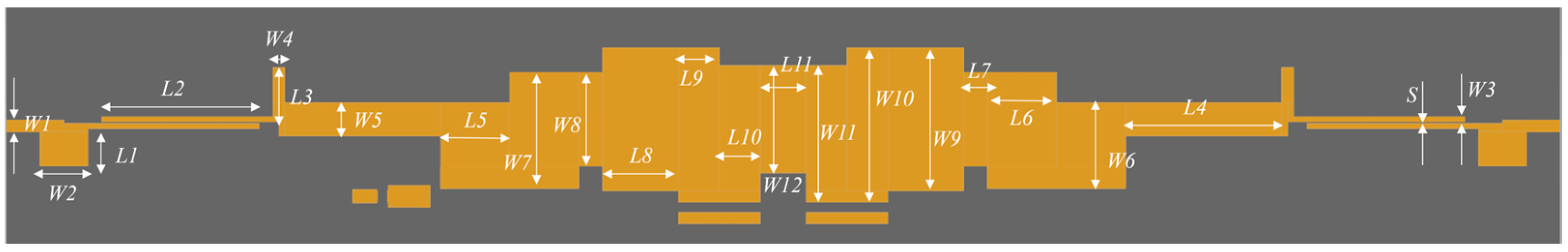
Figure 5. A detailed layout of the implemented switch, including all critical dimensions, is shown in
Figure 6, with exact values summarized in
Table 1. The design is fabricated on Rogers RO4534 (
≈ 3.4, tanδ ≈ 0.0027) with a thickness of 60 mil (1.524 mm), ensuring both low PIM and stable dielectric performance.
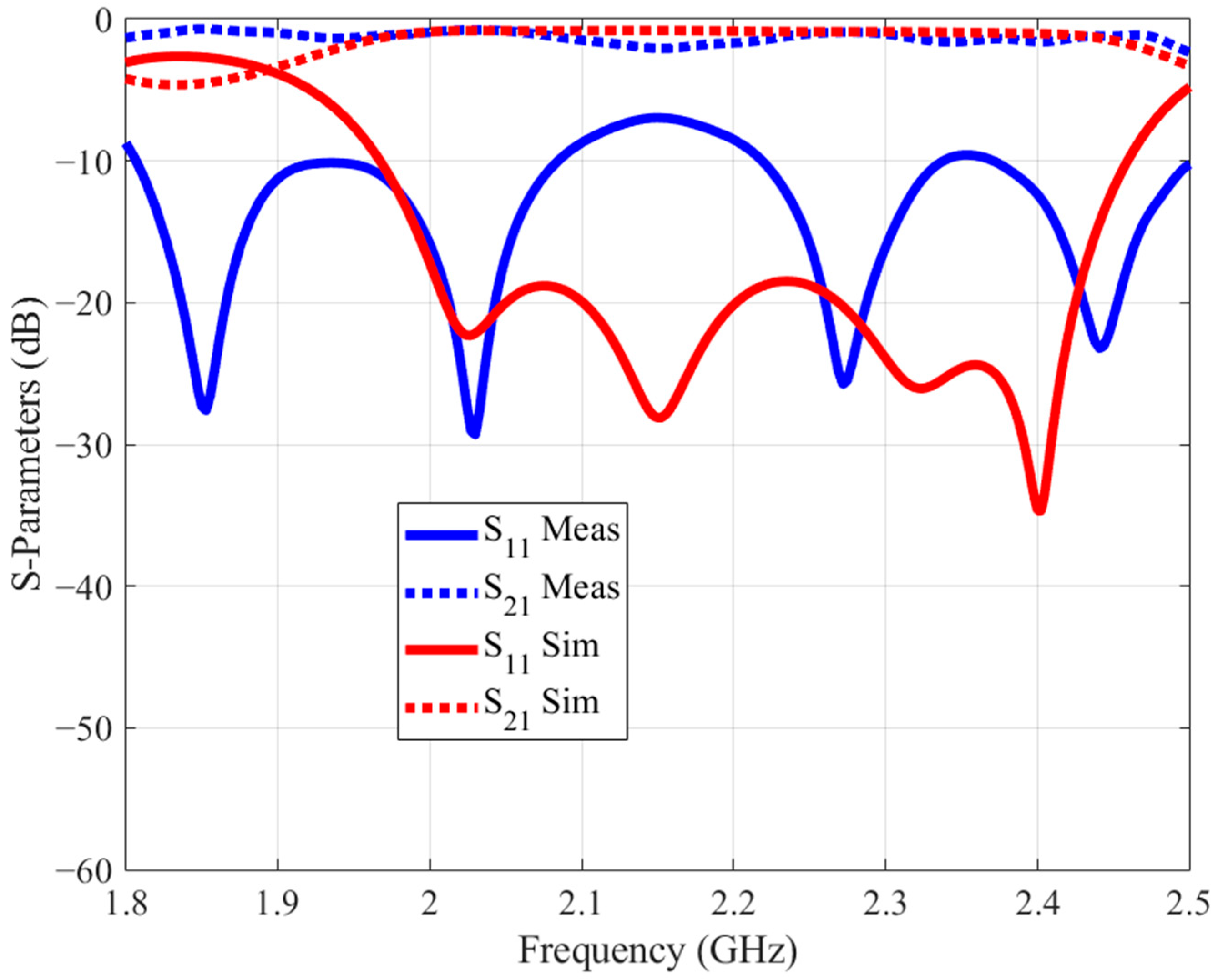
To evaluate the performance of the proposed design, the phase shift in the proposed structure was both simulated and measured, as shown in
Figure 7. The target phase shift of 45 degrees was successfully achieved, as confirmed by both simulation and measurement results. Additionally, the return loss (S
11) and insertion loss (S
21) were analyzed for both switching states of the PIN diodes. The corresponding simulated and measured results are presented in
Figure 8 for the OFF state and
Figure 9 for the ON state.
The provided results of the S-parameters show a discrepancy between simulation and measurement. During standalone measurements of the PIN diodes on a simple 50 Ω microstrip line, we observed that different samples of the same PIN diode model exhibited slight variations in their parasitic parameters. On the other hand, slight variations in the parasitic elements of different PIN diode samples become more pronounced in our design due to the intentionally reduced impedance seen by the diodes. This effect partly explains the minor discrepancies observed between simulations and measurements.
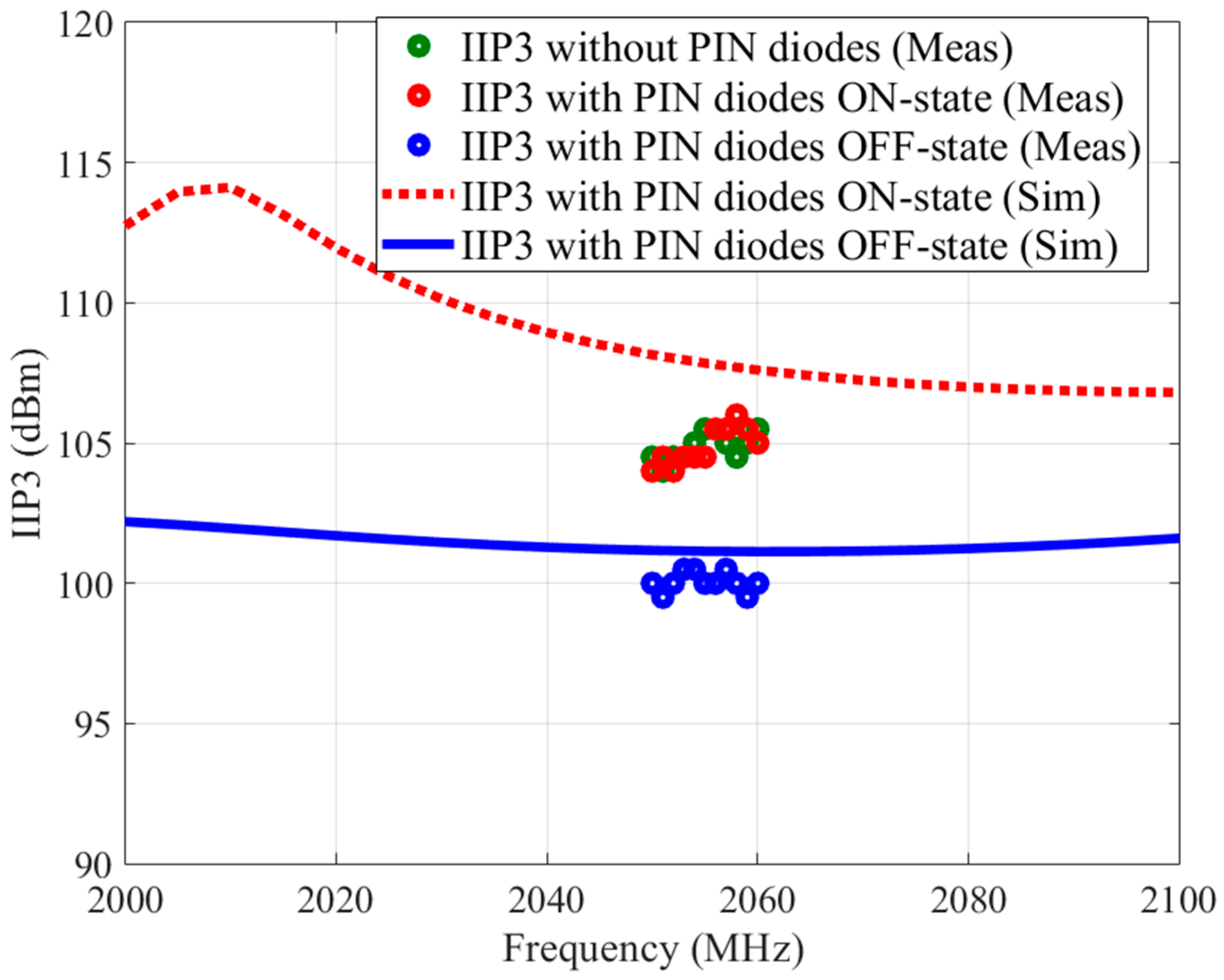
The linearity performance of the proposed design was evaluated under three different scenarios: (i) without PIN diodes, (ii) with PIN diodes in the ON state, and (iii) with PIN diodes in the OFF state. The corresponding simulated and measured results are presented in
Figure 10. All IIP3 measurements were conducted at an input power level of 25 W.
In the first scenario, the structure without PIN diodes exhibited a measured IIP3 of 106 dBm, primarily limited by the measurement setup. With the PIN diodes in the ON state, the simulated IIP3 was 108 dBm, while the measured value was 106 dBm—again constrained by the linearity of the test equipment. When the PIN diodes were in the OFF state, the simulated IIP3 was 101 dBm, and the measured result was 100 dBm, demonstrating strong agreement with simulation and confirming the effectiveness of the impedance-transformed parallel topology in improving linearity.
5. Discussion
A comparison of the key parameters of the proposed design with existing state-of-the-art solutions is summarized in
Table 2. The results clearly demonstrate that the proposed phase shifter achieves superior linearity performance.
Beyond the comparison, this work highlights important design trade-offs inherent in optimizing phase shifters for shared high-power Tx/Rx systems. Additionally, small parasitic variations among PIN diode samples were found to have a magnified impact under reduced impedance, emphasizing the value of precise diode characterization. The proposed methodology, though demonstrated here around 2 GHz for cellular phased arrays, is directly scalable to higher-frequency systems such as C-band radar or 5G mm wave arrays with appropriate coupler scaling and diode selection. Future work could explore integration with multi-bit phase controls or advanced switching elements like GaN PINs to further enhance linearity and power handling. Scaling to multi-bit implementations can be achieved by cascading additional loaded-line sections along the main transmission line, each independently biased to enable discrete phase control. Careful DC network isolation and impedance tuning are required to preserve linearity and minimize insertion loss.
The measured IIP3 exceeded +100 dBm, constrained by the test setup linearity. This practical limitation suggests that the actual device linearity may be even higher. Such extremely high IIP3 ensures ample margin for integration into phased array systems, where typical system-level requirements are significantly lower.
Future investigations could extend this work by characterizing the design under temperature variations, which affect PIN diode carrier dynamics and can impact both insertion loss and linearity. Similarly, adapting the design for wideband applications would involve optimizing the impedance transformers and accounting for frequency-dependent parasitic effects through broadband modeling and simulation.
6. Conclusions
This paper presented the design and implementation of a highly linear loaded-line digital phase shifter. The proposed architecture combines the use of PIN diodes in a parallel-to-ground configuration with impedance transformers to enhance linearity performance. This approach enabled the development of a one-bit phase shifter achieving an IIP3 exceeding 100 dBm. A prototype was designed, fabricated, and experimentally validated, with both simulation and measurement results confirming the intended 45-degree phase shift. The findings demonstrate that the integration of parallel PIN diodes with optimized impedance matching and layout design yields a compact, low-loss, and highly linear phase shifter—well-suited for modern RF and full-duplex communication systems. Future work may involve translating these high-linearity phase shifter designs to mm-wave frequencies to support advanced 5G and radar phased array applications.
Author Contributions
Conceptualization, F.G.; methodology, F.G. and A.D.; software, F.G.; validation, F.G. and A.D.; formal analysis, F.G. and J.Z.; investigation, F.G.; resources, F.G. and A.D.; data curation, F.G.; writing—original draft preparation, F.G.; writing—review and editing, J.Z. and Y.H.; visualization, F.G.; supervision, J.Z. and Y.H.; project administration, J.Z.; funding acquisition, J.Z. and Y.H. All authors have read and agreed to the published version of the manuscript.
Funding
This research received no external funding.
Institutional Review Board Statement
Not applicable.
Informed Consent Statement
Not applicable.
Data Availability Statement
The original contributions presented in this study are included in the article.
Conflicts of Interest
The authors declare no conflict of interest.
References
- Katanbaf, M.; Chu, K.-D.; Zhang, T.; Su, C.; Rudell, J.C. Two-Way Traffic Ahead: RF\/Analog Self-Interference Cancellation Techniques and the Challenges for Future Integrated Full-Duplex Transceivers. IEEE Microw. Mag. 2019, 20, 22–35. [Google Scholar] [CrossRef]
- Ghorbani, F.; Dayan, A.; Zhou, J.; Huang, Y.; Schuchinsky, A.; Gustafsson, M. Linearity Enhancement in PIN-Diode-Based Switches. IEEE Trans. Microw. Theory Tech. 2024, 73, 789–800. [Google Scholar] [CrossRef]
- Ghorbani, F.; Zhou, J.; Huang, Y.; Gustafsson, M. Impedance-Oriented Approach for Maximizing Linearity in pin-Diode-Based Phase Shifters. IEEE Trans. Microw. Theory Tech. 2025, 99, 1–10. [Google Scholar] [CrossRef]
- Liu, F.; Xu, J.; Duan, Y.-W.; Wan, H.; Zhang, H.; Zhu, L. A 5-Bit Digital Phase Shifter Using Phase-Tuning Property of Open-/Short-Circuit Microstrip Line-Loaded Slot Line Structure. IEEE Trans. Microw. Theory Tech. 2022, 71, 2605–2615. [Google Scholar] [CrossRef]
- Louati, S.; Boutayeb, H.; Hettak, K.; Talbi, L. New reconfigurable SIW phase shifter with transverse CPW-based stubs and PIN Diodes. In Proceedings of the 2022 IEEE International Symposium on Antennas and Propagation and USNC-URSI Radio Science Meeting (AP-S/URSI), Denver, CO, USA, 10–15 July 2022; pp. 850–851. [Google Scholar]
- Louati, S.; Talbi, L.; Hettak, K.; Boutayeb, H. 28 GHz Digital SIW Phase Shifter Using Embedded PIN Diodes. In Proceedings of the 2022 IEEE International Symposium on Antennas and Propagation and USNC-URSI Radio Science Meeting (AP-S/URSI), Denver, CO, USA, 10–15 July 2022; pp. 848–849. [Google Scholar]
- Franky Dakam Wappi, B.M.; Boutayeb, H.; Talbi, L. Reconfigurable Half Mode Substrate Integrated Waveguide Phase Shifter. In Proceedings of the EuCap, Florence, Italy, 26–31 March 2023. [Google Scholar]
- Longhi, P.E.; Colangeli, S.; Ciccognani, W.; Das, A.; Sharma, S.; Sharma, S.S.; Limiti, E. 32 dBm IP1dB/46 dBm IIP3 GaN Phase-Amplitude Setting Circuit at Ku-Band. IEEE Trans. Circuits Syst. II Express Briefs 2023, 71, 1849–1853. [Google Scholar] [CrossRef]
- Ghorbani, F.; Zhou, J.; Gustafsson, M.; Huang, Y. Highly Linear Phase Shifter with L-Topology PIN Diode-Based Switch. In Proceedings of the 2024 54th European Microwave Conference (EuMC), Paris, France, 24–26 September 2024; pp. 1012–1015. [Google Scholar]
- Kumar, R. A review on RF micro-electro-mechanical-systems (MEMS) switch for radio frequency applications. Microsyst. Technol. 2021, 27, 2525–2542. [Google Scholar]
- Wainstein, N.; Ankonina, G.; Swoboda, T.; Rojo, M.M.; Kvatinsky, S.; Yalon, E. Indirectly Heated Switch as a Platform for Nanosecond Probing of Phase Transition Properties in Chalcogenides. IEEE Trans. Electron Devices 2021, 68, 1298–1303. [Google Scholar] [CrossRef]
- Vander Missen, Z.; Macheret, S.; Semnani, A.; Peroulis, D. Plasma Switch-Based Technology for High-Speed and High-Power Impedance Tuning. In Proceedings of the 2021 IEEE 21st Annu. Wireless and Microwave Technology Conf. (WAMICON), Sand Key, FL, USA, 28–29 April 2021; pp. 1–4. [Google Scholar]
- Yasir, M.; Bistarelli, S.; Cataldo, A.; Bozzi, M.; Perregrini, L.; Bellucci, S. Tunable phase shifter based on few-layer graphene flakes. IEEE Microw. Wirel. Compon. Lett. 2018, 29, 47–49. [Google Scholar] [CrossRef]
- Caverly, R.H. Microwave and RF Semiconductor Control Device Modeling; Artech House: Norwood, MA, USA, 2016. [Google Scholar]
- Seo, W.; Kim, S.; Ko, B.; Jhon, H.; Kim, J. High-powered RF SOI switch with fast switching time for TDD mobile applications. IEEE Access 2023, 11, 7277–7282. [Google Scholar] [CrossRef]
- Mattsson, M. Intermodulation Distortion in Active and Passive Components; Chalmers Tekniska Hogskola: Gothenburg, Sweden, 2023. [Google Scholar]
- Eliasson, G. Performance of 2-18 GHz RF Switches Implemented in Chip & Wire Technology: Analysis of Switch Topologies, Bias Networks and an In-Depth EM Analysis of Bondwires. 2023. Available online: https://kth.diva-portal.org/smash/get/diva2:1834176/FULLTEXT01.pdf (accessed on 22 July 2025).
- Rikan, B.S.; Kim, D.; Choi, K.-D.; Hejazi, A.; Yoo, J.-M.; Pu, Y.; Kim, S.; Huh, H.; Jung, Y.; Lee, K.-Y. T/R RF switch with 150 ns switching time and over 100 dBc IMD for wideband mobile applications in thick oxide SOI process. Sensors 2022, 22, 507. [Google Scholar] [CrossRef] [PubMed]
- Ghorbani, F.; Zhou, J.; Gustafsson, M.; Huang, Y. Linearity of PIN Diode Switch in Both ON-state and OFF-state. In Proceedings of the 53rd European Microwave Conference, Berlin, Germany, 19–21 September 2023. [Google Scholar]
- Stephanson, B.; Caverly, R.H. Impact of Surface Effects on RF Switching PIN Diodes. In Proceedings of the 2021 IEEE Radio and Wireless Symposium (RWS), San Diego, CA, USA, 17–22 January 2021; pp. 144–146. [Google Scholar]
- Dayan, A.; Ghorbani, F.; Huang, Y.; Zhou, J.; Gustafsson, M.; Schuchinsky, A. Intermodulation Mitigation through Surrounding Impedance Manipulation. In Proceedings of the 2024 18th European Conference on Antennas and Propagation (EuCAP), Glascow, UK, 17–22 March 2024. [Google Scholar]
- Caverly, R.H.; Hiller, G. Distortion in microwave and RF switches by reverse biased PIN diodes. In Proceedings of the IEEE MTT-S International Microwave Symposium Digest, Long Beach, CA, USA, 13–15 June 1989; pp. 1073–1076. [Google Scholar]
- Drozdovskaia, L. RF frequency properties of a reverse biased thick switching PIN-diode. In Proceedings of the RAWCON 2000. 2000 IEEE Radio and Wireless Conference (Cat. No. 00EX404), Denver, CO, USA, 13 September 2000; pp. 147–150. [Google Scholar]
- Drozdovskaia, L. RF and microwave frequency properties of a reverse-biased thick switching PIN diode. IEEE Trans. Microw. Theory Tech. 2001, 49, 1370–1373. [Google Scholar] [CrossRef]
- Sze, S.M.; Li, Y.; Ng, K.K. Physics of Semiconductor Devices; John Wiley & Sons: Hoboken, NJ, USA, 2021. [Google Scholar]
- Bahl, I.; Gupta, K. Design of loaded-line pin diode phase shifter circuits. IEEE Trans. Microw. Theory Tech. 1980, 28, 219–224. [Google Scholar] [CrossRef]
- Stauss, G.H. Intrinsic Sources of IM Generation; NRL Memorandum Report 4233; Naval Research Lab: Washington, DC, USA, 7 July 1980.
- Reiss, W. Volterra series representation of a forward-biased pin diode. IEEE Trans. Electron Devices 1981, 28, 1495–1500. [Google Scholar] [CrossRef]
- Amin, F.; Liu, Y.; Zhao, Y.; Hu, S. Compact and low-loss phase shifters and multibit phase shifters based on inverted-E topology. IEEE Trans. Microw. Theory Tech. 2021, 69, 2120–2129. [Google Scholar] [CrossRef]
| Disclaimer/Publisher’s Note: The statements, opinions and data contained in all publications are solely those of the individual author(s) and contributor(s) and not of MDPI and/or the editor(s). MDPI and/or the editor(s) disclaim responsibility for any injury to people or property resulting from any ideas, methods, instructions or products referred to in the content. |
© 2025 by the authors. Licensee MDPI, Basel, Switzerland. This article is an open access article distributed under the terms and conditions of the Creative Commons Attribution (CC BY) license (https://creativecommons.org/licenses/by/4.0/).


