Abstract
For Convolutional Neural Networks (CNNs), Depthwise Separable CNN (DSCNN) is the preferred architecture for Application Specific Integrated Circuit (ASIC) implementation on edge devices. It benefits from a multi-mode approximate multiplier proposed in this work. The proposed approximate multiplier uses two 4-bit multiplication operations to implement a 12-bit multiplication operation by reusing the same multiplier array. With this approximate multiplier, sequential multiplication operations are pipelined in a modified DSCNN to fully utilize the Processing Element (PE) array in the convolutional layer. Two versions of Approximate-DSCNN (A-DSCNN) accelerators were implemented on TSMC 40 nm CMOS process with a supply voltage of 0.9 V. At a clock frequency of 200 MHz, the designs achieve 4.78 GOPs/mW and 4.89 GOP/mW power efficiency while occupying 1.16 mm and 0.398 mm area, respectively.
1. Introduction
In today’s age of technological development, Artificial Intelligence (AI) has become seamlessly integrated into society. In the past, AI computing relied on high-performance cloud computing, in which data is transmitted to a high-performance server for remote processing before being returned to their origin. Multiple penalties are incurred with this process; latency is a major concern and affects the ability of the local device to make timely decisions.
Therefore, the current development of the IC industry in AI is gradually moving toward the direction in which edge devices can operate independently. The design development of such devices is moving towards lower power consumption, higher throughput, and a smaller area. Amongst various reasons for this development are portable devices; higher power dissipation impacts the longevity of battery-operated devices, further limiting practical applications. This is why low-power chips are significant.
To address these issues, the improvement of the design of the PE as one of the basic elements in a CNN accelerator needs to be considered. This centers around the utilization of a configurable systolic array [1]. Although dataflow efficiency is enhanced through this approach, the fundamental computations within the PE remain unchanged. The dominant aspect in the PE’s basic computations is the multiplication operation, affecting area, latency, and power. This is where the incorporation of approximate computation methods using approximate multipliers becomes crucial for enhancing the PE design. However, the utilization of approximate multipliers may introduce other drawbacks to the overall network, including accuracy degradation and increased delay. This is where the contributions of this work come into play. A novel A-DSCNN architecture is proposed, integrating a new approximate multiplier, which seamlessly integrates into a modified DSCNN. In the implemented A-DSCNN, accuracy is maintained while efficiency is improved.
This paper is mainly motivated by the above and implements a new hardware architecture dedicated to the CNN model. The method of further optimizing the circuit in this paper is to reduce the circuit’s power consumption while limiting precision loss by simplifying and improving the architecture using approximate calculation methods.
Section 2 summarizes the background of CNN and DSCNN. Section 3 discusses the proposed DSCNN. The main contribution of this work is to propose a DSCNN employing a multi-mode approximate multiplier to reduce the number of computations and parameters. Then, through data scheduling and optimizing computations, the timing of the proposed A-DSCNN is further improved. Section 4 introduces this paper’s experimental method and performance results. Upon completion of the hardware implementation, it is benchmarked against other CNN hardware designs. Analysis of the results is detailed towards the end of this Section. Finally, Section 5 reviews the architecture and ideas proposed in this paper.
2. Related Works
2.1. Convolutional Neural Network (CNN)
A CNN consists of convolution layers, pooling layers, fully connected layers, and flattened layers. Compared with multi-layers neural networks, also known as multilayer perceptrons, CNN has fewer parameters. Another prominent feature of a CNN is that it can retain the location information of the image. In general, an image will have a certain degree of correlation between adjacent pixels.
2.2. Approximate Neural Networks
In this section, the focus is on introducing approximate arithmetic circuits employed in neural networks. The main objective is to explore the application of various approximate circuits or algorithms within neural network models. By utilizing these approximate circuits, it is anticipated that overall performance can be optimized while minimizing hardware requirements. This research direction holds significant growth potential, as it aims to reduce hardware complexity and associated costs while ensuring the integrity of the Neural Network remains intact.
Karnaugh map simplification is utilized by [2,3,4] for the implementation of digital circuitry that performs approximate arithmetic within a tolerable range. Using newer logic units or adders with improved architectures is proposed by [5,6]. The former proposes a Lower-Part-OR Adder architecture, while the latter reorganizes different adders through re-grouping modules coupled with design changes to optimize dataflow. Approximate arithmetic operators for Multiply-Accumulate (MAC) operators, which encompass the critical path of CNN models, are introduced by [7]. The high speed of N-way paths is leveraged by the proposed accelerator architecture. An approximation is implemented through hardware architecture improvements by [8,9].
The data flow of CNN processing and the energy efficiency achieved using a 2D systolic array architecture were discussed in [10]. An accelerator named Eyeriss for CNN was proposed in this paper, which optimized the data flow between each PE. However, the data flow of Eyeriss restricted the PE of diagonal input data feature sharing and the lateral way of weight kernel sharing.
Additionally, the Run Length Compression proposed in [10] also resulted in additional power consumption. Next, a priority-driven CNN accelerator optimized for a weight kernel was proposed in [11], where the modules were designed to work in parallel, fully utilizing the kernel and input image data. In this work, there was no need to design additional specific circuits, since weight sharing was unnecessary. As a result, power consumption and the chip area were reduced.
In [12], a unique approximation operation method was proposed. The approximate operation was initially performed through sampling to determine the location of the value that the pooling layer may retain. Selective convolution was performed by merging the pooling and convolutional layers, reducing redundant convolution operations. However, since this method required pre-processing the data, it was necessary to consider the penalties incurred from the additional encoder.
2.3. Depthwise Separable Convolution (DSC)
Another type of architecture that improves upon a CNN is Depthwise Separable Convolution (DSC). To reduce the high computational complexity required by CNN, Google utilizes a novel computational structure in MobileNet, aiming to decrease the computational cost of a CNN model [13].
MobileNet is a faster CNN architecture and a smaller model incorporating a new convolutional layer known as DSC. Due to their compact size, these models are particularly suitable for implementation in mobile and embedded devices. This approach primarily divides the original convolution into two separate parts: Depthwise Convolution (DWC) and Pointwise Convolution (PWC), enabling a reduction in computational requirements without compromising the underlying structure.
The difference between DSCNN and conventional CNN lies in the approach of the DWC. In DWC, the convolution kernel is split into a single-channel form, as illustrated in Figure 1. For each channel of the input data, a filter of size k is established, and separate convolution operations are performed on each channel without altering the depth of the input feature image. However, this process imposes a limitation on the expansion of the feature map’s size, thereby restricting the dimensionality of the feature map. Consequently, using PWC becomes necessary to combine the outputs of the DWC and generate a new feature map.
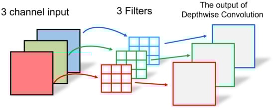
Figure 1.
Illustration of Depthwise Convolution (DWC).
PWC essentially represents a convolution, as illustrated in Figure 2, and its operational method is similar to traditional convolution. The kernel size in PWC is , where the parameter M corresponds to the number of channels in the previous layer of the DWC.
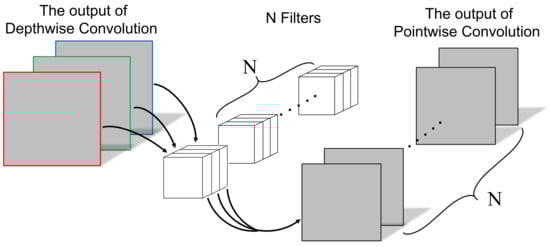
Figure 2.
Illustration of Pointwise Convolution (PWC).
Subsequently, PWC combines the feature maps from the previous step along the depth dimension, generating new feature maps based on the number of kernels. The output of both operations is equivalent to that of a conventional convolutional layer.
PWC serves two primary purposes: firstly, it enables DSCNN to adjust the number of output channels, and secondly, it consolidates the output feature maps from DWC. The preference for DSCNN over conventional CNN arises from its significant reduction in computational requirements and parameters, resulting in improved computational efficiency. While a slight decrease in accuracy can be expected with DSCNN, the deviation remains within an acceptable margin.
As shown in Figure 3, the number of parameters and calculations of conventional CNN is and , respectively. Meanwhile, the number of computations and parameters in a DSCNN, which comprises both depthwise convolution and pointwise convolution, is and . By simplifying the aforementioned equations, the ratio of parameters and computations in a DSCNN compared to a conventional CNN can be estimated in Equation (1).
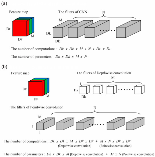
Figure 3.
The parameter and computation in (a) Conventional Convolutional Neural Network, and (b) Depthwise Separable CNN.
The main objective of this work is to have conventional CNN replaced by DSCNN as the primary architecture to reduce the number of computations and parameters, thereby significantly decreasing power consumption.
Subsequently, introductions to some related papers are provided. In [14], an accelerator design for reconfigurable DSCNN is proposed. However, it is plagued by low hardware utilization rates and timing delays encountered during each feature map reconstruction.
In [15], an adaptive row-based dataflow of a unified reconfigurable engine for DSC is proposed. However, due to its reconfigurable nature, it suffers from low hardware utilization and energy efficiency.
An architecture for energy-efficient convolutional units for DSC is presented in [16]. This architecture implements array-based PE to optimize the workloads of PWC and DWC. The paper also introduces a reconfigurable multiplier array with a coefficient to optimize data reads. Nevertheless, challenges are encountered regarding low hardware utilization and energy efficiency due to the proposed configurable multiplier array. Furthermore, the paper primarily focuses on optimizing PWC, resulting in a lower utilization rate of the PE during DWC and leading to timing and hardware reuse issues.
The framework known as DSCNN is utilized in most of the aforementioned reviewed papers, aiming to enhance overall performance compared to conventional CNN. However, in some papers, the original characteristics of DSCNN are disregarded due to the complex design of layer optimization in neural networks. As a result, a new DSCNN architecture is proposed in this work for neural network image recognition. It involves the combination of DSCNN with the approximate operation method and implementing a complete hardware architecture on the ASIC.
3. Proposed Method
The proposed method, A-DSCNN, will be discussed in this section.
3.1. Multi-Mode Approximate Multiplier
The multi-mode approximate multiplier proposed in this paper is depicted in Figure 4. The original multiplier circuit is divided into two blocks using a control signal alternating between two operation modes. This paper’s image and weight input data are partitioned into two parts: the MSB part and the LSB part. Mode-0 is employed to compute the LSB, while Mode-1 is utilized for the MSB.
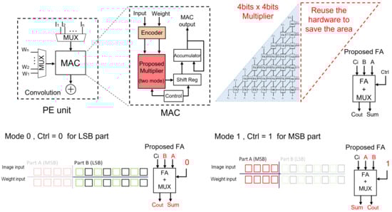
Figure 4.
Approximate multiplier’s operation.
The MSB portion takes precedence in this work, as it plays a more critical role in the computation. Conventional multiplication is employed for this part, ensuring that no subsequent errors are introduced. On the other hand, the LSB portion utilizes an encoder to calculate the LSBs and divides the value into two-digit groups. Considering only the larger even-numbered bits as the new value reduces the computational complexity from 8-bit to 4-bit. Since the proposed approximate multiplier matches this 4-bit computation, the existing hardware can be repurposed by adding control signals. This results in a reduction in chip area and power dissipation, thereby achieving lower power consumption.
The operation of the approximate multiplier involves dividing it into the MSB and LSB parts using a control signal. For the LSB part, the control signal is set to 0, activating Mode-0 of the multiplier for calculations. Conversely, for the MSB part, the control signal is set to 1, initiating Mode-1 for calculations. Since the same internal circuitry is utilized, the same multiplier hardware array can be reused. A shift register is employed to output the bits correctly to perform two consecutive 4-bit × 4-bit multiplications. Consequently, compared to a conventional multiplier, the proposed multiplier offers reduced power consumption and occupies less area.
To ensure the functionality and identify potential errors in the multipliers, the designs of both the approximate and standard multipliers undergo synthesis and mapping to the specific process technology, namely TSMC CMOS. This allows for gate-level simulations to be conducted.
To verify the performance of the multipliers, random numbers are generated and used to test both the approximate and standard multipliers. The results of these multiplications are compared to the ideal multiplication results, as expressed in Equation (2) [17]. This comparison helps evaluate the accuracy and reliability of the multipliers under consideration.
where k random numbers are used, with m multiplicands and n multipliers generating products through the approximate or standard multiplier circuits, compared to the ideal product . The multiplication operations are carried out using signed integers 12 bits to match the truncation performed by the approximate multiplier. For this specific evaluation, k is set to 10,000, and it has been observed that the errors do not significantly increase for higher values of k, but a large computation resource is required for the circuit simulation.
Table 1 summarizes the comparison between the approximate multiplier and the standard multiplier. Under the random number test, the multiplication error for the approximate multiplier is found to be 1.2% higher than that of the standard multiplier. These results confirm that the approximate multiplier can be successfully integrated into the CNN architecture.

Table 1.
Comparison of Approximate Multiplier and Standard Multiplier.
3.2. DSCNN with Multi-Mode Approximate Multiplier
The proposed approach involves scheduling Mode-1 and Mode-0 to operate sequentially, utilizing the same multiplier, thereby creating a multi-mode approximate multiplier. This multiplier is then integrated into a DSCNN, leading to novel hardware architecture known as A-DSCNN. The implemented hardware incorporates the approximate computations mentioned earlier and employs a pipelined scheduling strategy, which is illustrated in Figure 5 for a typical convolutional layer implemented in A-DSCNN.
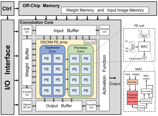
Figure 5.
Hardware structure of a convolutional layer in A-DSCNN (PE: Processing Element).
The operation of the convolution core is given as follows:
- Initially, the image input and weight inputs are loaded from an off-chip memory by the control unit and stored in the input buffer and weight buffer, respectively.
- The encoder control determines whether the input buffer and weight buffer data should undergo encoding, and accordingly, the reformatted data are obtained.
- The reformatted data are then supplied to the convolution core in the A-DSCNN PE array for computation.
- The convolution control unit within the A-DSCNN PE array decides whether to perform depthwise convolution and pointwise convolution, generating a new job.
- The newly created job comprises a set of instructions pipelined for processing.
- After scheduling, individual instructions are sent to the multi-mode approximate multiplier for computation. Control signals determine if the computed data need to be shifted.
- Once the computations are complete, the computed results are accumulated and sent back to the output buffer to finalize the convolution operation.
Timing is often not considered in conventional DSCNN, as observed in [16]. As a result, the operation process follows the same approach as conventional CNN, where the system waits for the input to be read before proceeding to the next convolution step. To address this timing issue, the computational steps are rescheduled to align with the new pipelined strategy, in addition to splitting the original convolution operation into the DWC and the PWC.
The timing sequence of the convolution operation is demonstrated with an example in Figure 6, considering one convolution operation. In this example, since the kernel size is 3 × 3, it is necessary to read in nine values for each convolution operation. In reference to [16], the MAC operation is not performed until the input is loaded onto the buffer. This approach leads to a sequential execution, where each step waits for the completion of the previous step before proceeding to the subsequent MAC step. Consequently, the overall runtime performance is adversely affected.
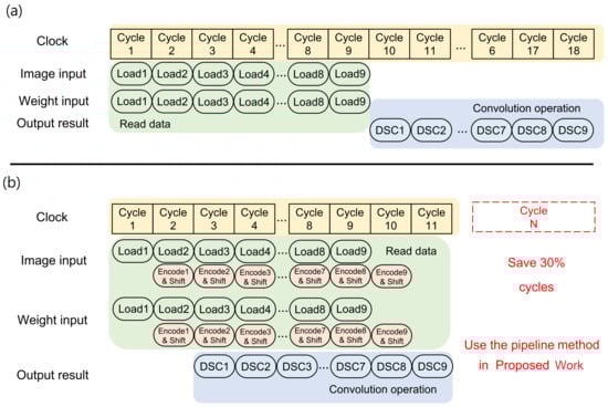
Figure 6.
Convolutional layer’s timing schematic of (a) Conventional DSCNN, and (b) Proposed A-DSCNN.
To overcome this limitation, jobs are scheduled to pipeline instructions in the proposed A-DSCNN approach, with the same MAC operation. With this method, computations can commence as soon as the first input is read, reducing the number of clock cycles required to complete the operation. As depicted in Figure 6, the number of cycles is reduced from 18 to 11 in comparison to conventional DSCNN [16]. Additionally, reusing hardware logic units further reduces the area required for implementation.
Before discussing the performance in the next section (Section 4), it is important to mention the design trade-off associated with the proposed A-DSCNN. Implementing the multi-mode approximate multiplier introduces overheads in the A-DSCNN, such as including control blocks (‘Control’ in Figure 4) and dedicated scheduling. Therefore, it is crucial to consider the timing of the A-DSCNN, as illustrated in Figure 6, when designing the scheduling scheme. This is followed by determining the operation of control blocks. The two-mode approximate multiplier offers a good compromise between accuracy, area and timing, although it is also possible to have a three-mode approximate multiplier.
4. Performance Results
Considering the relatively large size of the VGG16 model [18], a modified version of VGG (referred to as “VGGnet”) is employed as the initial hardware implementation for performance analysis. The image classification task will be performed using the CIFAR-10 dataset [19]. This modification is required to relax the requirement to perform the simulations, especially the circuit-level simulations.
The hardware architecture is designed using structured Verilog HDL. The operating frequency is set to 200 MHz during timing simulation, and the design is implemented during the TSMC 40-nm CMOS process. The operating frequency and technology are chosen to perform a compatible comparison with the existing work for benchmarking, Table 2, although it can be implemented at a lower technology node and higher operating frequency if desired. The table presents data on power consumption, area, and energy efficiency from various reference papers. According to the summarized information in Table 2, the proposed Approximate-DSCNN accelerators achieve approximately 20% higher power efficiency compared to the works recently reported in papers [20,21]. Additionally, the proposed accelerators occupy only 13% of the area of the design presented in [20]. It is worth mentioning that the design described in [21] also utilizes the VGG16 model. The entire hardware architecture is illustrated in the architecture diagram shown in Figure 7.
Table 2.
Comparison of A-DSCNN with Recent Accelerators.
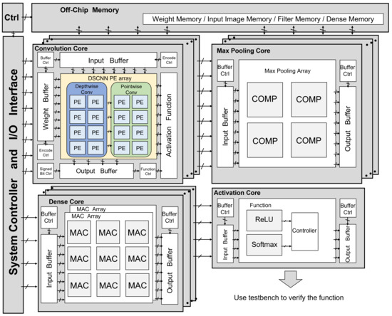
Figure 7.
The overall hardware architecture of A-DSCNN.
Table 3 provides additional details about the modified VGGnet model for the hardware implementation. With 7997 parameters, it is a smaller network with a slight accuracy penalty that is used primarily for verification. With its parameters quantized to 12-Bit, the total memory footprint of the network is 11.7 kB. Additionally, the VGG16 model presented here is the same model found in [18] with the conventional convolutional layers replaced with depthwise separable convolutional layers. This reduces the number of parameters to 20,595,585. The total memory footprint of the network is 29.46 MBs.
Table 3.
Model Architecture of VGG16 and Modified VGGnet.
In CNN architectures, the primary components of the PE are the multipliers and adders. This work focuses on key design considerations, including the proposed multiplier, latency, hardware reuse, and reduction of redundant computations.
To facilitate low latency dataflow, both internal and external buffers must be employed. Figure 7 highlights the necessary on/off chip buffers included in the design. When taking into consideration the size of the input/output feature maps, the primary constraint on the off-chip memory are the network parameters, as shown in Table 4. And as such, the size of the network employed would be the key consideration.
Table 4.
Size of Registers required for Internal Buffers.
The different on-chip buffers serve to reduce latency amongst the various cores. Table 4 contains a breakdown of the buffers used by the different cores, which is dictated by the largest layers within the network that employ the specific cores.
By addressing these design considerations, the proposed A-DSCNN (VGGnet) achieves significant savings in hardware resources, with a 53% reduction compared to conventional DSCNN [16]. The area reported in [16] is only for its convolutional layer, Table 2. Furthermore, the energy efficiency is improved by 1.56 times, resulting in an accelerator design with a smaller area and higher performance.
For the physical implementation of the chip, the Innovus software from Cadence [22] is utilized to perform the Place and Route (PnR) process, generating the layout file of the circuit. Other Electronic Design Automation (EDA) tools, such as VCS from Synopsys [23], are employed for chip simulation and functional verification.
Figure 8 showcases the completed A-DSCNN (VGG16) accelerator layout, while Table 5 outlines the specifications. With an operating frequency of 200 MHz, the accelerator core area is 1.16 mm. It operates at a 0.9 V supply voltage, resulting in power consumption of 486.81 mW.
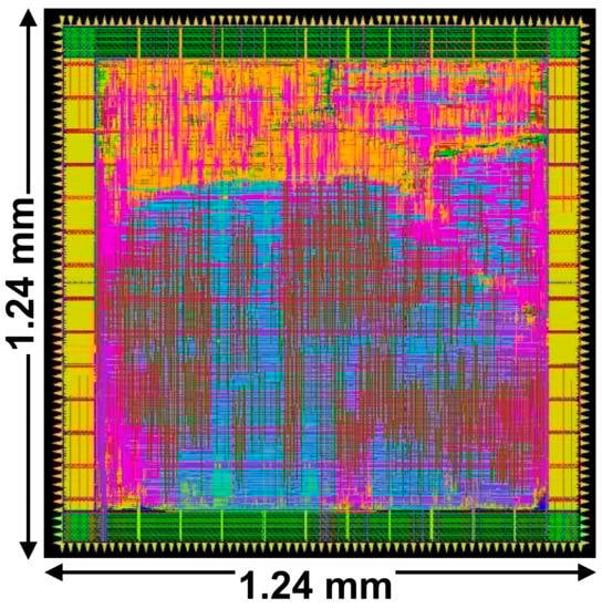
Figure 8.
A-DSCNN (VGG16) accelerator layout.
Table 5.
Proposed A-DSCNN (VGG16) Acceletor Specification.
The main components (convolutional, pooling, and dense layers) account for approximately 78% of the total area, while other components (registers and control units) make up the remaining 22%. The main components contribute to around 90% of the total power consumption, whereas other components (registers and control units) are responsible for the remaining 10%. The breakdowns are also summarized in Table 5.
5. Conclusions
This paper introduces a novel architecture called A-DSCNN, which aims to enhance the performance of CNN accelerators. The design’s key focus is replacing the conventional multiplier with a newly proposed approximate multiplier. This multiplier employs a mixed-precision algorithm to mitigate the negative effects of redundant computations. It is integrated into the A-DSCNN architecture using a unique pipeline scheduling method.
To validate the effectiveness of the proposed A-DSCNN, VGG16 is employed as the model, and the CIFAR-10 dataset is used for evaluation. The proposed design is implemented on the TSMC 40-nm CMOS process, operating at a supply voltage of 0.9 V.
From Table 2, it can be concluded that both of the proposed A-DSCNN (VGG16, VGGnet) accelerators have achieved superior power efficiency (GOPs/mW) and occupy less area compared to the recently reported accelerators.
Author Contributions
Conceptualization, J.-J.S., N.P. and T.H.T.; methodology, J.-J.S. and T.H.T.; software, J.-J.S. and T.H.T.; validation, N.P., J.-J.S., T.H.T. and I.-C.W.; formal analysis, J.-J.S. and T.H.T.; investigation, J.-J.S., T.H.T. and I.-C.W.; resources, T.H.T.; data curation, J.-J.S., N.P. and T.H.T.; writing—original draft preparation, J.-J.S., N.P. and T.H.T.; writing—review and editing, N.P., J.-J.S., T.H.T. and I.-C.W.; visualization, N.P. and J.-J.S.; supervision, T.H.T. and I.-C.W.; project administration, T.H.T.; funding acquisition, T.H.T. All authors have read and agreed to the published version of the manuscript.
Funding
This research received no external funding.
Data Availability Statement
Evaluation of this work was performed using the CIFAR-10 Dataset, which can be found at: https://www.cs.toronto.edu/~kriz/cifar.html (accessed on 2 February 2023).
Acknowledgments
The authors thank Lai I-Hong for his continuous technical support and for giving some suggestions through discussion to overcome the bottleneck encountered and make this study possible.
Conflicts of Interest
The authors declare no conflict of interest.
Abbreviations
The following abbreviations are used in this manuscript:
| A-DSCNN | Approximate-DSCNN. |
| AI | Artificial Intelligence. |
| ASIC | Application Specific Integrated Circuit. |
| CIFAR | Canadian Institute for Advanced Research. |
| CMOS | Complimentary Metal Oxide Semiconductor. |
| CNN | Convolutional Neural Network. |
| DSC | Depthwise Separable Convolution. |
| DSCNN | Depthwise Separable CNN. |
| DWC | Depthwise Convolution. |
| EDA | Electronic Design Automation. |
| HDL | Hardware Descriptor Language. |
| IC | Integrated Circuits. |
| LSB | Least Significant Bit. |
| MAC | Multiply-Accumulate. |
| MSB | Most Significant Bit. |
| PE | Processing Element. |
| PnR | Place and Route. |
| PWC | Pointwise Convolution. |
| ReLU | Rectified Linear Unit. |
| TSMC | Taiwan Semiconductor Manufacturing Company. |
| VGG | Visual Geometry Group. |
References
- Chua, S.H.; Teo, T.H.; Tiruye, M.A.; Wey, I.C. Systolic Array Based Convolutional Neural Network Inference on FPGA. In Proceedings of the 2022 IEEE 15th International Symposium on Embedded Multicore/Many-core Systems-on-Chip (MCSoC), Penang, Malaysia, 19–22 December 2022; pp. 128–133. [Google Scholar] [CrossRef]
- Kulkarni, P.; Gupta, P.; Ercegovac, M. Trading Accuracy for Power with an Underdesigned Multiplier Architecture. In Proceedings of the 2011 24th Internatioal Conference on VLSI Design, Chennai, India, 2–7 January 2011; pp. 346–351. [Google Scholar] [CrossRef]
- Shin, D.; Gupta, S.K. Approximate logic synthesis for error tolerant applications. In Proceedings of the 2010 Design, Automation and Test in Europe Conference and Exhibition (DATE 2010), Dresden, Germany, 8–12 March 2010; pp. 957–960. [Google Scholar] [CrossRef]
- Gupta, V.; Mohapatra, D.; Raghunathan, A.; Roy, K. Low-Power Digital Signal Processing Using Approximate Adders. IEEE Trans. Comput.-Aided Des. Integr. Circuits Syst. 2013, 32, 124–137. [Google Scholar] [CrossRef]
- Mahdiani, H.R.; Ahmadi, A.; Fakhraie, S.M.; Lucas, C. Bio-Inspired Imprecise Computational Blocks for Efficient VLSI Implementation of Soft-Computing Applications. IEEE Trans. Circuits Syst. I Regul. Pap. 2010, 57, 850–862. [Google Scholar] [CrossRef]
- Shin, D.; Gupta, S.K. A Re-design Technique for Datapath Modules in Error Tolerant Applications. In Proceedings of the 2008 17th Asian Test Symposium, Hokkaido, Japan, 24–27 November 2008; pp. 431–437. [Google Scholar] [CrossRef]
- Elbtity, M.E.; Son, H.W.; Lee, D.Y.; Kim, H. High Speed, Approximate Arithmetic Based Convolutional Neural Network Accelerator. In Proceedings of the 2020 International SoC Design Conference (ISOCC), Yeosu, Republic of Korea, 21–24 October 2020; pp. 71–72. [Google Scholar] [CrossRef]
- Jou, J.M.; Kuang, S.R.; Chen, R.D. Design of low-error fixed-width multipliers for DSP applications. IEEE Trans. Circuits Syst. II Analog. Digit. Signal Process. 1999, 46, 836–842. [Google Scholar] [CrossRef]
- Guo, C.; Zhang, L.; Zhou, X.; Qian, W.; Zhuo, C. A Reconfigurable Approximate Multiplier for Quantized CNN Applications. In Proceedings of the 2020 25th Asia and South Pacific Design Automation Conference (ASP-DAC), Beijing, China, 13–16 January 2020; pp. 235–240. [Google Scholar] [CrossRef]
- Chen, Y.H.; Krishna, T.; Emer, J.S.; Sze, V. Eyeriss: An Energy-Efficient Reconfigurable Accelerator for Deep Convolutional Neural Networks. IEEE J. Solid-State Circuits 2017, 52, 127–138. [Google Scholar] [CrossRef]
- Yue, J.; Liu, Y.; Yuan, Z.; Wang, Z.; Guo, Q.; Li, J.; Yang, C.; Yang, H. A 3.77TOPS/W Convolutional Neural Network Processor With Priority-Driven Kernel Optimization. IEEE Trans. Circuits Syst. II Express Briefs 2019, 66, 277–281. [Google Scholar] [CrossRef]
- Spagnolo, F.; Perri, S.; Corsonello, P. Approximate Down-Sampling Strategy for Power-Constrained Intelligent Systems. IEEE Access 2022, 10, 7073–7081. [Google Scholar] [CrossRef]
- Howard, A.G.; Zhu, M.; Chen, B.; Kalenichenko, D.; Wang, W.; Weyand, T.; Andreetto, M.; Adam, H. MobileNets: Efficient Convolutional Neural Networks for Mobile Vision Applications. arXiv 2017, arXiv:1704.04861. [Google Scholar] [CrossRef]
- Chen, Y.G.; Chiang, H.Y.; Hsu, C.W.; Hsieh, T.H.; Jou, J.Y. A Reconfigurable Accelerator Design for Quantized Depthwise Separable Convolutions. In Proceedings of the 2021 18th International SoC Design Conference (ISOCC), Jeju Island, Republic of Korea, 6–9 October 2021; pp. 290–291. [Google Scholar] [CrossRef]
- Li, B.; Wang, H.; Zhang, X.; Ren, J.; Liu, L.; Sun, H.; Zheng, N. Dynamic Dataflow Scheduling and Computation Mapping Techniques for Efficient Depthwise Separable Convolution Acceleration. IEEE Trans. Circuits Syst. I Regul. Pap. 2021, 68, 3279–3292. [Google Scholar] [CrossRef]
- Chong, Y.S.; Goh, W.L.; Ong, Y.S.; Nambiar, V.P.; Do, A.T. An Energy-Efficient Convolution Unit for Depthwise Separable Convolutional Neural Networks. In Proceedings of the 2021 IEEE International Symposium on Circuits and Systems (ISCAS), Daegu, Republic of Korea, 22–28 May 2021; pp. 1–5. [Google Scholar] [CrossRef]
- Balasubramanian, P.; Nayar, R.; Maskell, D.L. Approximate Array Multipliers. Electronics 2021, 10, 630. [Google Scholar] [CrossRef]
- Simonyan, K.; Zisserman, A. Very deep convolutional networks for large-scale image recognition. arXiv 2014, arXiv:1409.1556. [Google Scholar]
- Krizhevsky, A.; Hinton, G. Convolutional Deep Belief Networks on CIFAR-10. Master’s Thesis, University of Toronto, Toronto, ON, Canada, 2010. [Google Scholar]
- Lin, K.P.; Liu, J.H.; Wu, J.Y.; Liao, H.C.; Huang, C.T. VISTA: A 704mW 4K-UHD CNN Processor for Video and Image Spatial/Temporal Interpolation Acceleration. In Proceedings of the 2023 IEEE International Solid- State Circuits Conference (ISSCC), San Francisco, CA, USA, 19–23 February 2023; pp. 48–50. [Google Scholar] [CrossRef]
- Liu, X.; Cao, C.; Duan, S. A Low-Power Hardware Architecture for Real-Time CNN Computing. Sensors 2023, 23, 2045. [Google Scholar] [CrossRef] [PubMed]
- Cadence: Computational Software for Intelligent System Design. Available online: https://www.cadence.com/en_US/home.html (accessed on 30 March 2023).
- Synopsys: EDA Tools, Semiconductor IP and Application Security Solutions. Available online: https://www.synopsys.com/ (accessed on 30 March 2023).


Disclaimer/Publisher’s Note: The statements, opinions and data contained in all publications are solely those of the individual author(s) and contributor(s) and not of MDPI and/or the editor(s). MDPI and/or the editor(s) disclaim responsibility for any injury to people or property resulting from any ideas, methods, instructions or products referred to in the content. |
© 2023 by the authors. Licensee MDPI, Basel, Switzerland. This article is an open access article distributed under the terms and conditions of the Creative Commons Attribution (CC BY) license (https://creativecommons.org/licenses/by/4.0/).