Article

Standard-Cell-Based Comparators for Ultra-Low Voltage Applications: Analysis and Comparisons

by
Riccardo Della Sala
1,
Francesco Centurelli
1,
Giuseppe Scotti
1,* and
Gaetano Palumbo
2
1
Dipartimento di Ingegneria dell’Informazione, Elettronica e Telecomunicazioni (DIET), Università degli Studi di Roma “La Sapienza”, 00184 Rome, Italy
2
Dipartimento di Ingegneria Elettrica, Elettronica e Informatica (DIEEI), Università degli Studi di Catania, 95123 Catania, Italy
*
Author to whom correspondence should be addressed.
Chips 2023, 2(3), 173-194; https://doi.org/10.3390/chips2030011
Submission received: 18 April 2023 / Revised: 13 July 2023 / Accepted: 16 August 2023 / Published: 18 August 2023

Abstract

:
This work is focused on the performance of three different standard-cell-based comparator topologies, considering ultra-low-voltage (ULV) operation. The main application scenarios in which standard-cell-based comparators can be exploited are considered, and a set of figures of merit (FoM) to allow an in-depth comparison among the different topologies is introduced. Then, a set of simulation testbenches are defined in order to simulate and compare the considered topologies implemented in both a 130 nm technology and a 28 nm FDSOI CMOS process. Propagation delay, power consumption and power–delay product are evaluated for different values of the input common mode voltage, as a function of input differential amplitude, and in different supply voltage and temperature conditions. Monte Carlo simulations to evaluate the input offset voltage under mismatch variations are also provided. Simulation results show that the performances of the different comparator topologies are strongly dependent on the input common mode voltage, and that the best values for all the performance figures of merit are achieved by the comparator based on three-input NAND gates, with the only limitation being its non-rail-to-rail input common mode range (ICMR). The performances of the considered comparator topologies have also been simulated for different values of the supply voltage, ranging from 0.3 V to 1.2 V, showing that, even if standard-cell-based comparators can be operated at higher supply voltages by scaling their performances accordingly, the best values of the FoMs are achieved for V D D = 0.3 V.

1. Introduction

A latched comparator is a circuit element that interfaces the analog to the digital world: its output is either a low or high logic level, according to the relationship between the input signal, sampled by the latching clock, and a reference threshold. Often, a differential input signal with an implicit zero reference level is used, but fully differential comparators that have explicit differential inputs both for the signal and for the reference are also used [1,2,3,4,5,6].
The latched comparator is a key building block for many mixed-signal applications, and finds wide diffusion in systems such as analog-to-digital converters (ADCs), wireline receivers, memory bit-line detectors and digital low-dropout regulators (DLDOs) [3,7,8,9,10,11]. The comparator is usually composed of an input preamplifier followed by a latch, often combined in the StrongARM topology [12,13,14], where a clocked transconductor drives a pair of cross-coupled inverters by their sources or, in the double-tail topology [15,16,17,18], where the clocked preamplifier and the latch use separate tail current branches. It is worth noting that, for high frequency applications, Current-Mode Logic (CML) latches are also used [11,19,20,21,22].
From a designer’s point of view, the comparator is an analog block, and is typically designed according to the standard analog design flow. Indeed, both the schematic and the layout design phases are carried out manually, iterating each step until specifications are met with a suitable robustness under process, supply voltage and temperature (PVT) variations and mismatches. The overall design effort, however, is highly time-consuming when compared to the typical semi-automatic digital design flow, so that the design of analog blocks requires a large fraction of the overall effort, even if they constitute a small portion of the overall system. There is, therefore, a strong drive to innovate the analog design flow, making it compatible with the automatic place-and-route CAD tools and possibly also allowing automatic sizing of the devices [23,24,25,26,27,28].
Following the above-described context, research trends are towards designing analog blocks using digital standard cells, either to mimic the behavior of analog building blocks [29,30,31,32,33,34] or by implementing analog functions in the digital domain [7,9,10,35,36,37,38,39,40,41,42,43,44,45,46,47,48,49]. A standard-cell-based implementation of analog functions simplifies the portability of designs among different technologies, and the speed vs. supply voltage reconfigurability. In particular, the standard-cell-based approach is well suited to a ultra-low voltage (ULV) context, where stacking of several devices becomes very difficult, thus limiting the use of typical analog design techniques such as cascoding.
The usual approach to design standard-cell-based latched comparators starts from a NAND-based [3,6,7,8,46] or NOR-based latch [50,51], and several designs have been presented in the literature to optimize different performances for applications in ADCs and LDOs [9,10,49,52,53,54,55,56,57]. However, such applications typically focus on different performance parameters, hence proposed designs are not always easy to compare. In this work, we analyze the main application scenarios for latched comparators to derive the performance parameters of interest and, hence, some suitably tailored figures of merit to evaluate and compare designs. We then review the main topologies for standard-cell-based latched comparators presented in the literature from these different viewpoints, defining a standardized characterization setup. This allows evaluating the suitability of the different topologies to the different application scenarios, and devising design guidelines for the optimization of comparators.
The paper is structured as follows: performance parameters and application scenarios are presented in Section 2, a review of the main standard-cell-based comparator topologies is reported in Section 3, whereas the simulation testbench and the figures of merit defined in this work to compare the different topologies in the different application scenarios are presented in Section 4. The results of the simulations and a comparative analysis are reported in Section 5 and Section 6, respectively. Finally, some conclusions are drawn in Section 7.

2. Latched Comparators: Performance Parameters and Application Scenarios

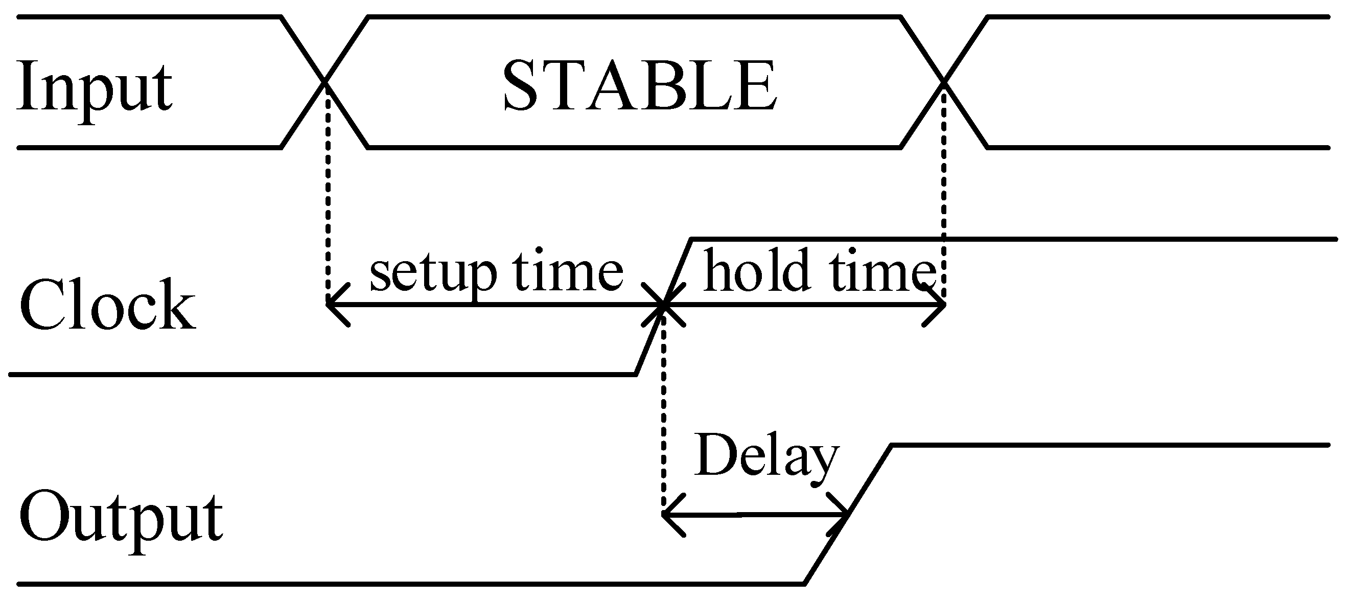
2.1. Performance Parameters of the Latched Comparator

Several performance parameters can be defined to characterize the latched comparator, and they mostly concern its resolution, speed and energy consumption. The clock-to-output propagation time is defined as the comparator delay [16,58,59,60]: it measures the time that intercurs from the latching edge of the clock signal to the time when the output voltage can be identified as one of the logic levels (50% of the transition). The comparator delay sets the maximum speed of the comparator.
Other time-related parameters, shown in Figure 1, are the setup and hold times, defined as the time intervals where the input signal has to keep a stable value (or at least remain constantly above or below the reference), before and after the latching clock edge, respectively.
From the power dissipation point of view, the latched comparators do not typically have a static current. Power ( P D ) is dissipated during latching and reset phases, i.e., in correspondence with positive and negative clock edges, and is usually measured as energy per conversion. Power consumption is often combined with the comparator delay (i.e., P D · D e l a y ) to define the Power–Delay Product (PDP).
The comparator is used to establish if the input signal is above or below a given threshold, hence important performance parameters are related to its resolution, i.e., the minimum difference between signal and threshold that the comparator is able to resolve [61]. Several phenomena affect the comparator resolution. First of all, the time needed to settle the output to a logic level increases when the difference between the input and the reference gets smaller, tending to infinity when such difference goes to zero. Hence, for a finite available decision time, there is a minimum signal that can be resolved, and it is called the comparator sensitivity. For lower inputs, the comparator enters a metastable state [62,63,64,65], i.e., its output is neither a logic 1 nor a logic 0, and is strongly affected by other factors (memory effect, noise, disturbances, etc.).
Comparator resolution is also affected by offset and noise. The comparator offset, due to device mismatches, can be seen as a random signal that adds to the input, altering the comparison with the reference [60,66]. Noise in the comparator is important when the input signal is small and the comparator is near its tripping point, thus resulting in a linear periodically time-varying (LPTV) process [60,67,68].
Further performance parameters refer to the input interface of the comparator. In fact, in applications where the comparator interfaces with a capacitive source, its dynamic input current can alter the value of the charge stored in the capacitors [61,69], and its input capacitance is seen in parallel to the source capacitance, affecting the voltage-to-charge conversion. Moreover, the comparator behavior and performance is generally dependent on its input common-mode voltage, and a parameter of importance in some applications is the comparator input common mode range (ICMR).

2.2. Performance Parameters vs. Latched Comparators Applications

The main application fields of standard-cell-based latched comparators are analog-to-digital converters and digital LDOs. Whereas some performance parameters are important in all those cases, the different application scenarios pose different requirements on the comparator.
Stochastic flash ADCs [3,7,70,71,72] were one of the first architectures considered for standard-cell-based implementation. Basically, a large number of nominally identical comparators (i.e., with the same reference level) are used, and the statistical distribution of the offset is used to map the input voltage level in the output code. In this case, the standard deviation of the offset of the comparators sets the input voltage range of the ADC, hence a large offset dispersion results in an advantage. On the other hand, other performance parameters are of little importance, including the ICMR, since all the comparators use the same reference level (in a single-ended implementation, the common-mode voltage of the comparator is set by the reference level).
For all the other (non-stochastic) ADC architectures, sensitivity, offset and noise levels are very important specifications, and have to be compatible with the required resolution of the overall ADC. Typically specifications on noise and offset are very stringent, whereas the comparator sensitivity results often much lower than practical values of the quantization levels; in this case, since sensitivity reduces in lower comparison times, designers can trade sensitivity for speed.
The requirements on ICMR are, instead, heavily dependent on the architectural details. In particular, flash ADCs use several comparators with different reference levels; hence, a large ICMR is required, unless a fully differential implementation is adopted. Focusing on successive-approximation-register (SAR) ADCs, details of the implementation make the difference. In a single-ended implementation, a solution where the input signal is sampled and compared with the DAC output [9] requires a large ICMR, whereas the implementation exploiting a capacitive DAC that is also used to sample the input signal, so that Vin-Vdac is compared with a fixed reference, has no ICMR requirement. The differential implementation generally features a capacitive DAC also used to sample the input signal, and compares the Vin-Vdac difference with an implicit zero reference level. This typically poses no requirement on the ICMR of the comparator, unless the set-and-down algorithm [73] is exploited. In this case, to minimize power consumption, such an algorithm acts on a single side of the differential capacitive DAC, thus also affecting the input common mode of the comparator, which evolves towards the bottom end of the input range as the conversion of each sample proceeds. If a rail-to-rail input range is considered, with an input common mode of V D D / 2 , an ICMR from 0 to V D D / 2 is required. SAR ADCs with a capacitive DAC are affected by the input capacitance of the comparator, which has to be minimized, and by kickback noise, i.e., the dynamic input current of the comparator in correspondence of clock edges.
Discrete-time sigma-delta ADCs [51,74] are a further architecture where standard-cell-based latched comparators find an application: in this case, a single fixed reference voltage is used in a 1-bit quantizer; thus, requirements on both the comparator resolution and the ICMR are relaxed.
In the case of digital LDOs [10,46,47,48,49], a single comparator is used to compare the output voltage with the reference which, however, could be variable, with the aim of generating an adjustable output voltage. Requirements on the comparator resolution, i.e., offset and noise, are set by the acceptable ripple and error on the output voltage, and are typically less stringent than the requirements found for high-resolution ADCs. The need for a variable reference determines the specification for the ICMR.
Other requirements, such as comparator delay, energy per conversion and area footprint, are strongly dependent on the application, but their minimization can be always considered an important design goal.

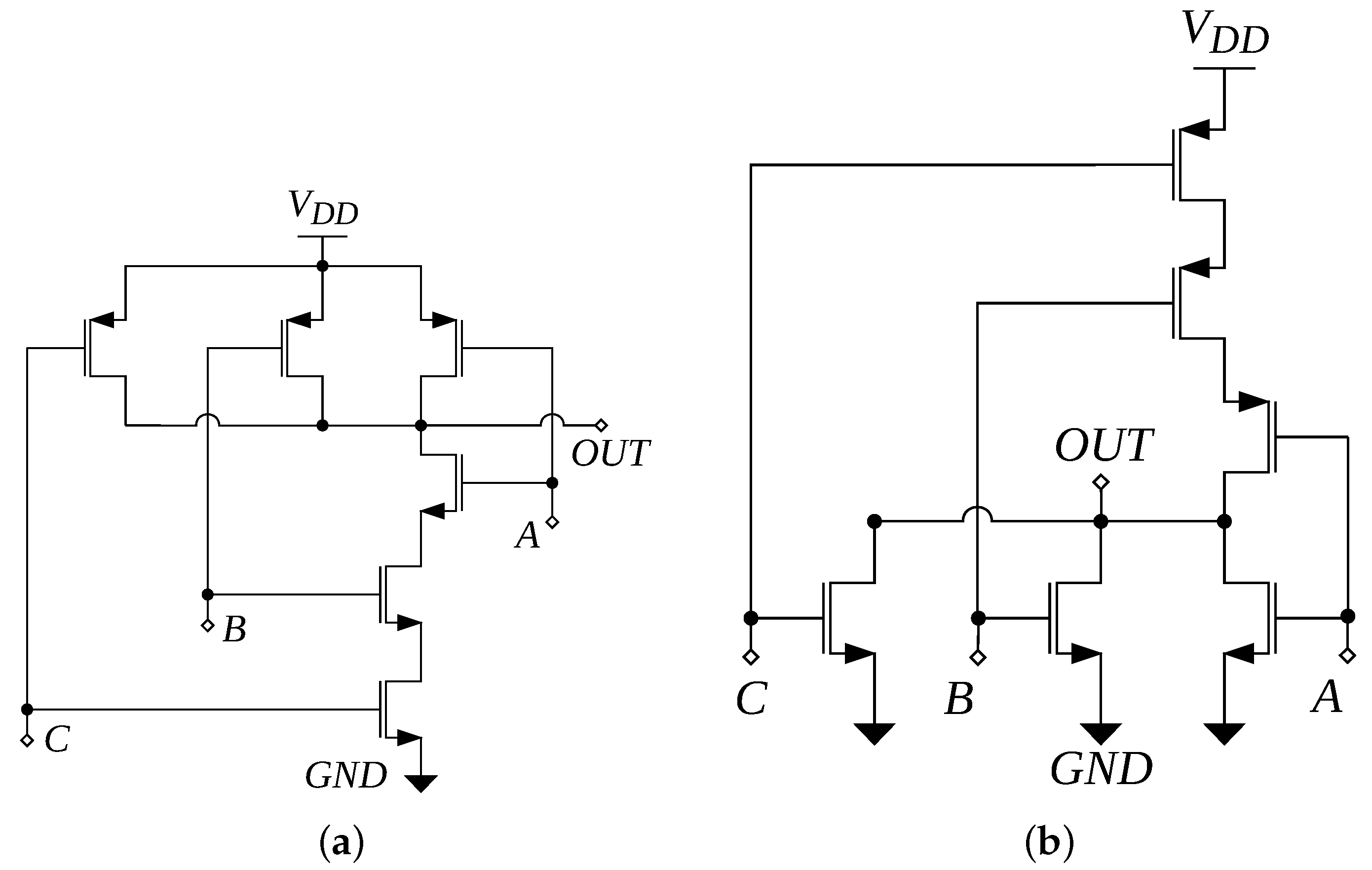
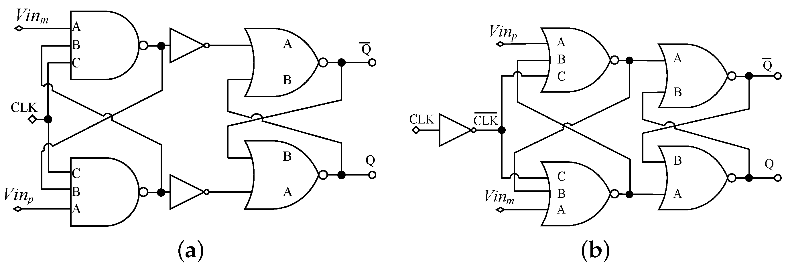
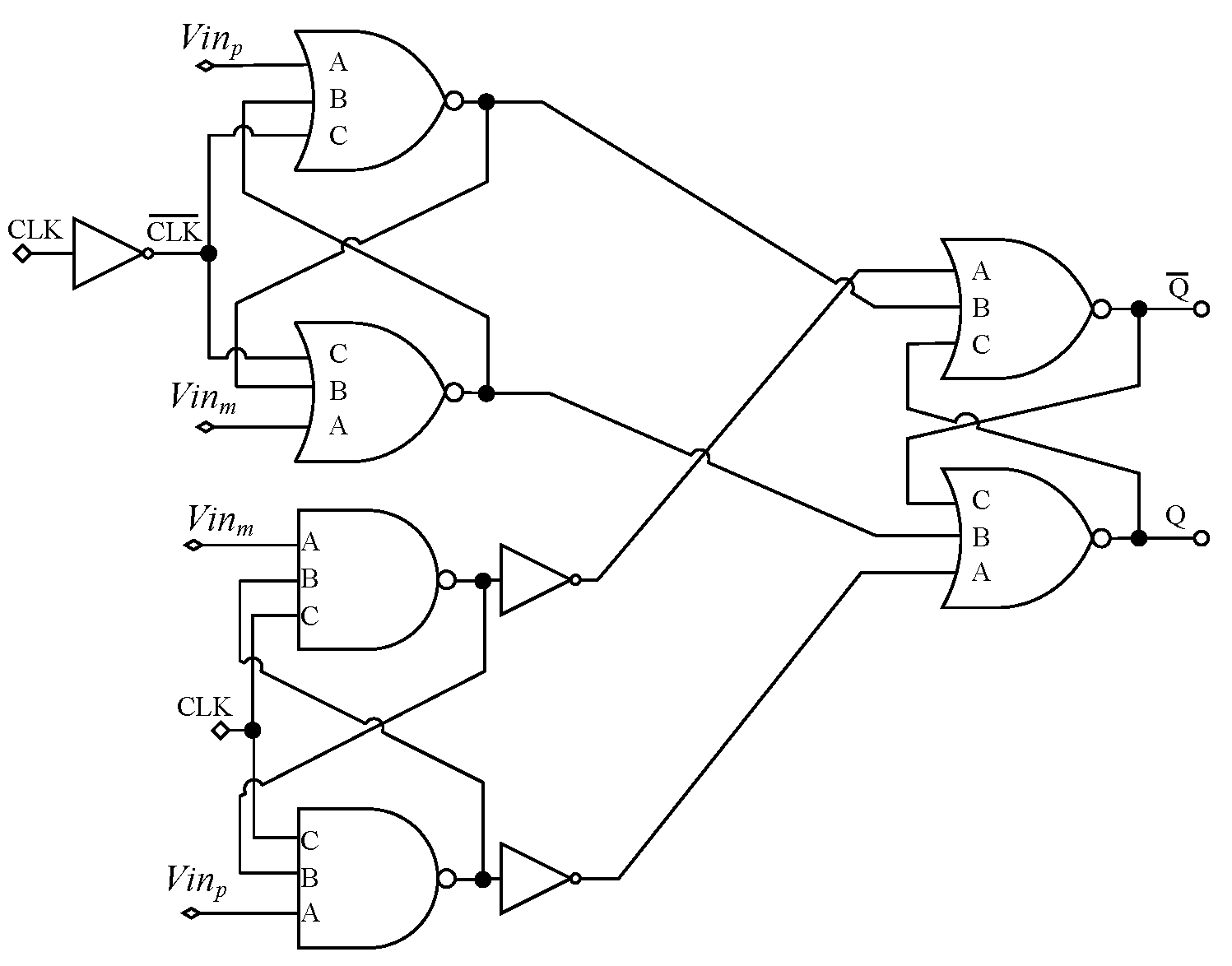
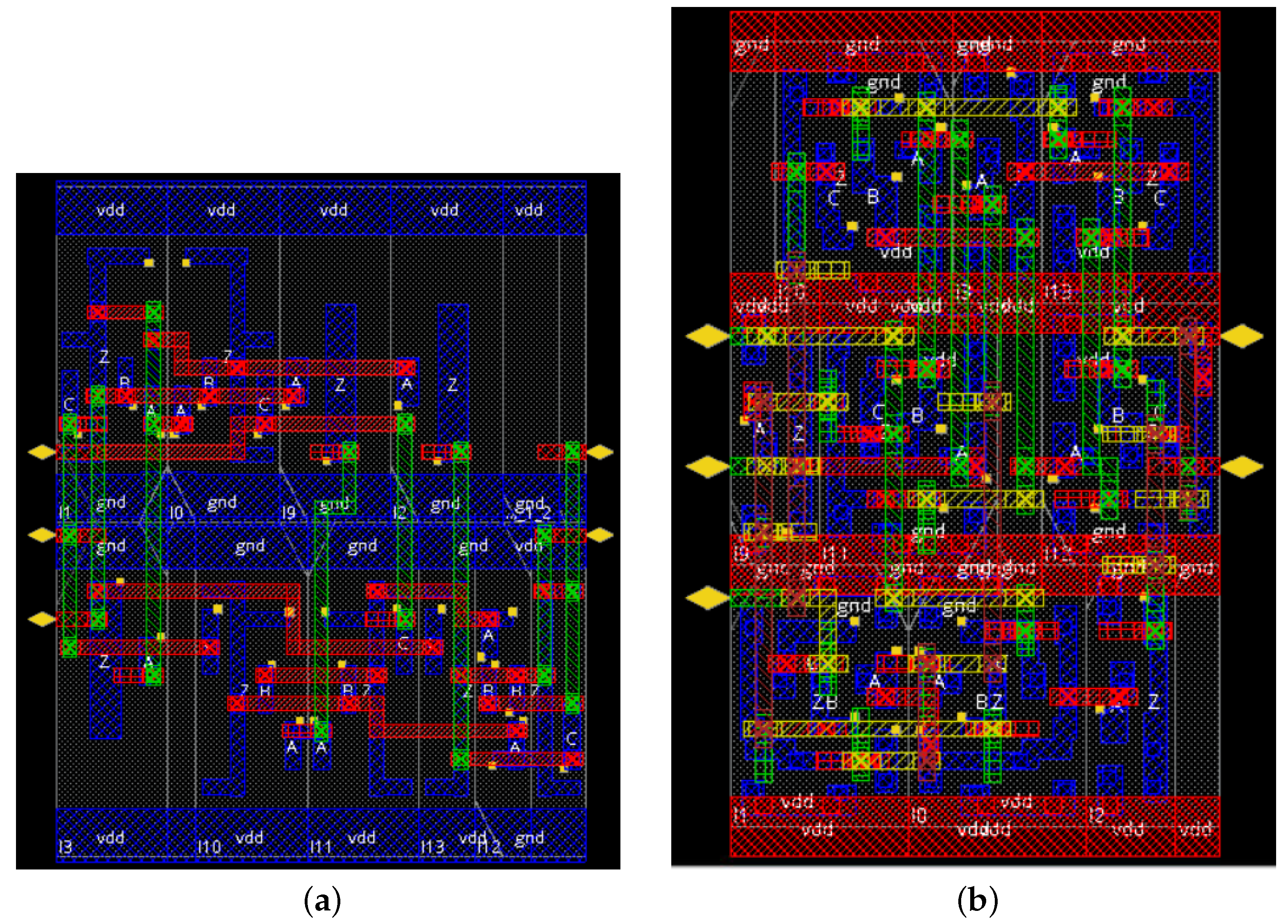
3. A Review of the Main Topologies to Implement Standard-Cell-Based Dynamic Voltage Comparators

The first standard-cell-based comparator was proposed in [7], and is the one depicted in Figure 2a (denoted as a N A N D 3 -based comparator in the following figure). It is composed of a first stage, made up of two N A N D 3 cells, and a second-stage N O R latch that samples and holds the output of the first stage. The two input terminals of the comparator are connected to the A input of the two N A N D 3 gates. The differential input signal results are therefore amplified by the N A N D 3 and by the following N O T gates.
The N O R 3 -based version of the standard-cell-based comparator proposed in [7] is shown in Figure 2b ( N O R 3 -based comparator in the following figure). In this circuit, the two input terminals of the comparator are connected to the A input of the two N O R 3 gates. The differential input signal results amplified only by the N O R 3 gates, resulting in lower gain than in the N A N D 3 -based comparator. The transistor level schematics of the N A N D 3 and N O R 3 gates are reported in Figure 3a,b, respectively, showing the connections of the input, the clock and the feedback signals.
As discussed in [55], the ICMR of the comparator in Figure 2a is limited to voltages larger than V D D / 2 , whereas lower voltages cause the comparator to stop operating. In a similar way, a dual issue occurs for the comparator in Figure 2b, in which the ICMR is limited to voltages lower than V D D / 2 .
The above limitations to the ICMR for the comparators in Figure 2a,b can be overcome by using the rail-to-rail comparator presented in [52,55] and shown in Figure 4 (rail-to-rail comparator in the following figure). The comparator in Figure 4 combines the digital outputs of the N A N D 3 and N O R 3 -based comparators in a complementary way, as in rail-to-rail analog operational amplifiers. It has to be pointed out that this paper focuses on comparators which do not require specific gates, which may have different schematic-level implementations in the different technologies and libraries and, therefore, can be implemented in all the digital standard-cell libraries. In particular, since the comparator proposed in [53] exploits the specific schematic level implementation of the AOI and OAI gates, which is, in general, different in the different standard-cell libraries, we have not included this circuit in the comparisons.

4. Simulation Testbench and Figures of Merit

In order to test the performance of the comparators reported in [7,52,55] we have carried out simulations referring to the standard-cells library of both a 130 nm bulk-CMOS process and a 28 nm fully depleted silicon on insulator (FDSOI) CMOS technology from STMicroelectronics, in the Cadence Virtuoso environment. More specifically, a high-performance library based on a low threshold voltage and high speed transistors has been adopted for the 130 nm technology, whereas and an high-density library based on standard threshold voltage and low leakage transistors has been chosen for the 28 nm technology. Each comparator output has been loaded by a minimum size inverter taken from the standard-cells library, as is typically performed for measuring the propagation delays of digital gates. To carry out a fair comparison, the minimum size standard-cells have been adopted to implement all the comparator topologies. A supply voltage of 0.3 V has been assumed to compare the different topologies working in a ULV regime, as deduced by literature applications of standard-cell-based comparators. Further, to provide more complete information to the reader, a technology comparison for 0.6 V, 0.9 V and 1.2 V (especially this last two values now not represent ULV operation) has been carried out on the 130 nm CMOS.

4.1. Testbench Description

An ad hoc testbench has been designed to characterize the main performance parameters of the standard-cell comparators. In this section, we explain in detail how the main performance parameters have been evaluated.

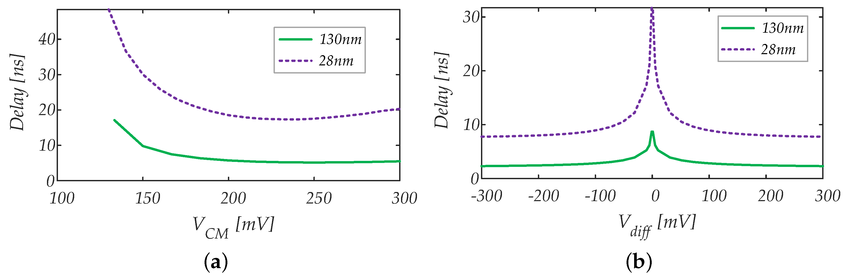
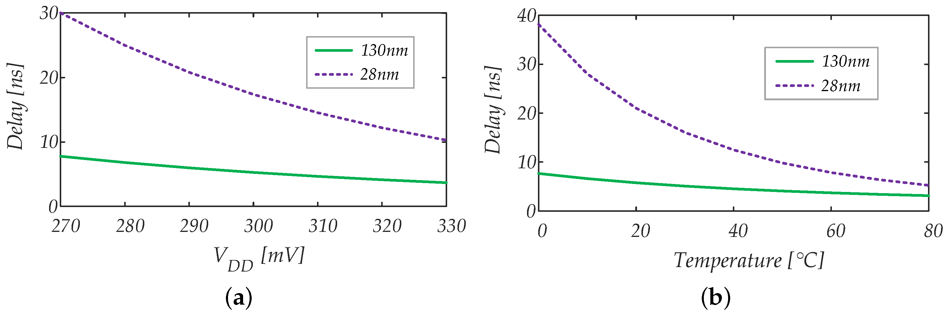
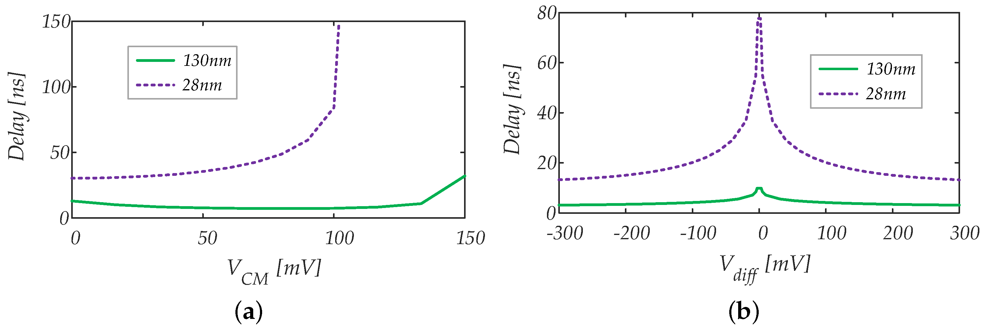
4.1.1. Propagation Delay vs. Input Common Mode Voltage

The clock-to-output propagation delay of the different comparators has been evaluated with considering different input common mode voltages in the following test conditions:
  • Supply voltage V D D = 0.3 V;
  • Input common mode varied in the range between 0 and V D D ;
  • Differential input signal amplitude of 10 mV;
  • Temperature of 27 °C.
The differential input signal amplitude of 10 mV has been assumed as a trade-off between a very small input signal (i.e., high sensitivity) and speed.

4.1.2. Propagation Delay vs. Input Differential Signal Amplitude

The clock-to-output propagation delay characteristic versus the input differential signal amplitude has been carried out with considering the following parameters:
  • V D D = 0.3 V;
  • Input common mode voltage set at V D D 4 , V D D 2 and 3 V D D 4 ;
  • Temperature set at 27 °C.
The three points, V D D 4 , V D D 2 and 3 V D D 4 , have been chosen to sample the ICMR, because they represent the midpoint of the ideal ICMR of the N O R 3 , rail-to-rail and N A N D 3 comparators, respectively.

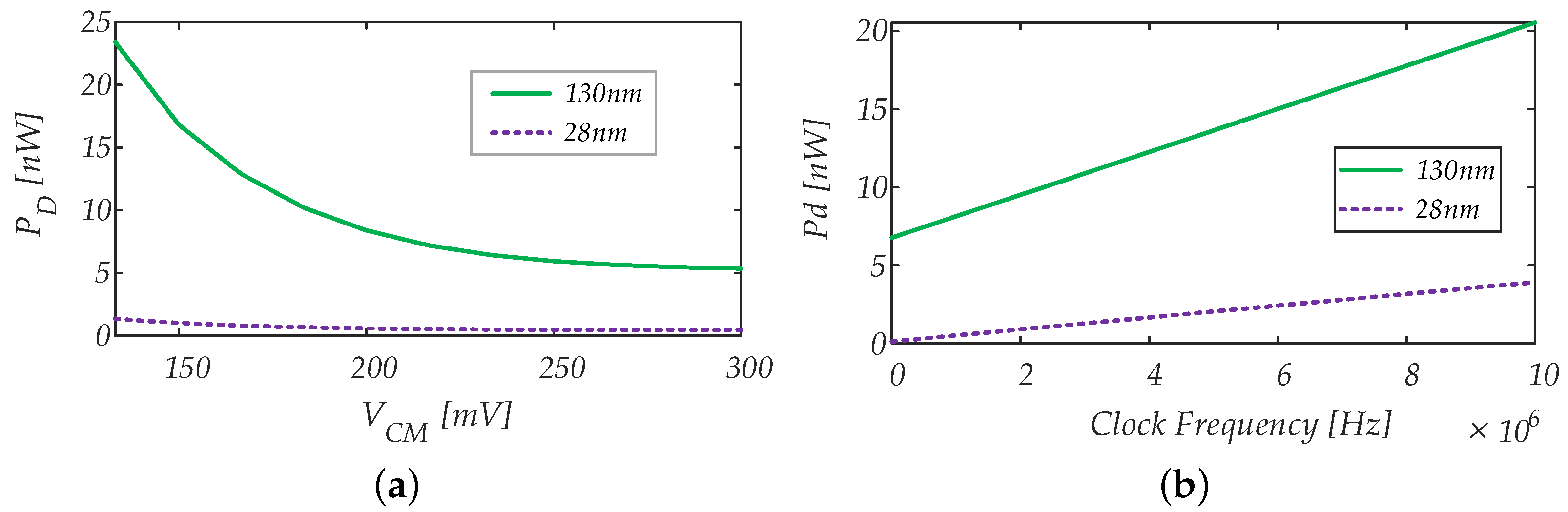
4.1.3. Power Consumption vs. Input Common Mode Voltage, Supply Voltage and Temperature Variations

The power consumption versus the input common mode voltage has been estimated with considering:
  • V D D = 0.3 V ± 10%;
  • A differential input signal amplitude of 10 mV;
  • A clock frequency set at 10 Hz and at 10 MHz;
  • A temperature varying from 0 to 80 °C.
The clock frequency set at 10 Hz is in agreement with previous works dealing with ULV standard-cell-based comparators. Since we have found that for such a low clock frequency, static power is not negligible, to better compare the different topologies, we have also computed power consumption at a frequency of 10 MHz, which has been chosen as a frequency in which power consumption is dominated by dynamic power and at which all comparators can reliably operate. The temperature range has been chosen in agreement with several papers dealing with ULV circuits [75,76,77], as well as the supply voltage variation.

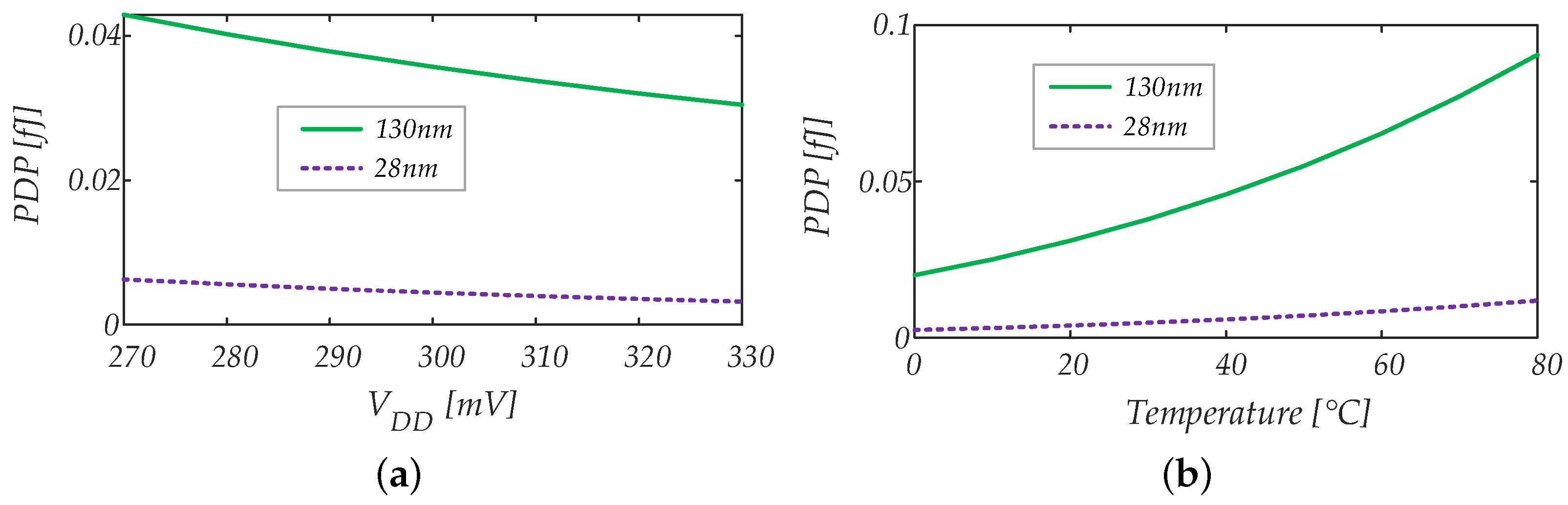
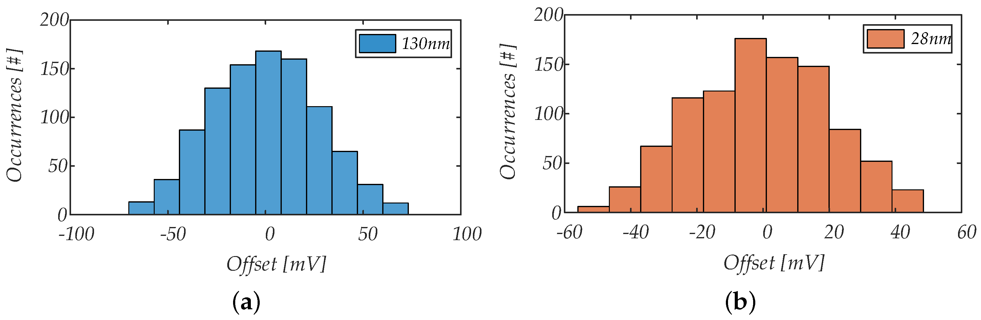
4.1.4. Input Offset Voltage vs. Supply Voltage, Temperature and Mismatch Variations

The input offset voltage of the comparators has been evaluated in the following conditions:
  • V D D = 0.3 V;
  • An input signal varying linearly with time in a transient simulation;
  • A differential input signal amplitude ranging from −70 mV to +70 mV;
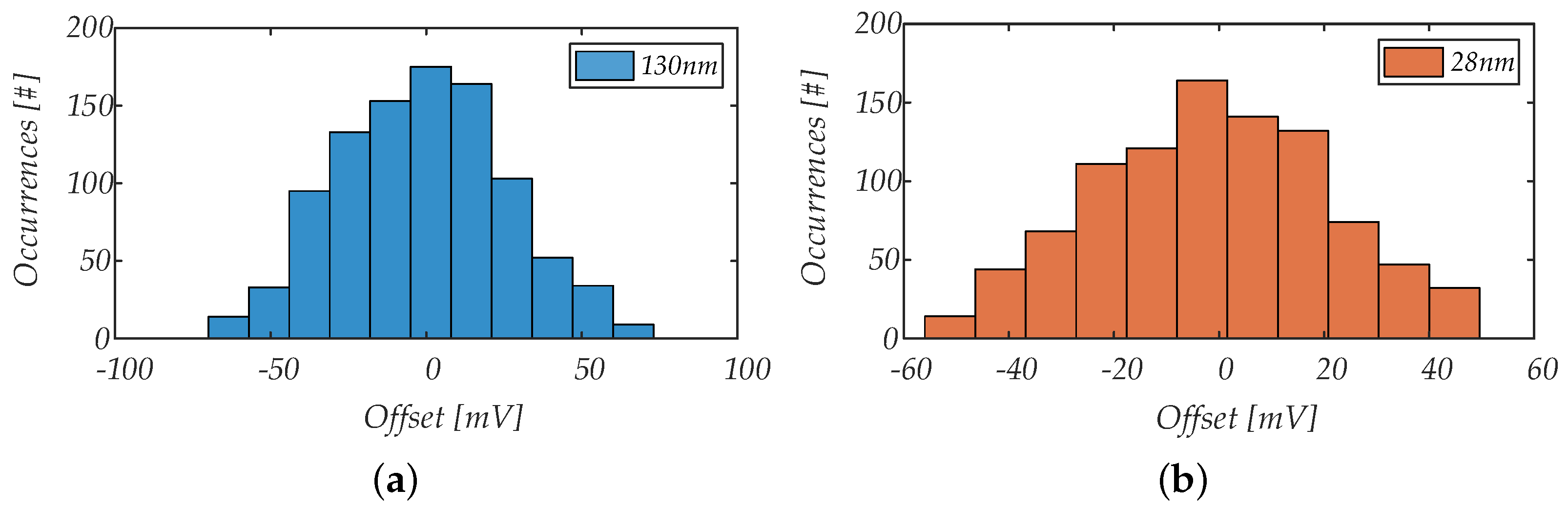
  • Monte Carlo simulations using statistical models provided by IC manufacturers are used to account for technology mismatches;
  • 1000 Monte Carlo runs have been performed on each topology.

4.2. Figures of Merit Definition

The Power–Delay Product (PDP) is a commonly adopted parameter to quantify how good the trade-off between speed performance and power consumption is, and is also used in the context of comparator design. Even if the PDP is useful to quantify the performance of comparators in almost all ADC and LDO applications, it does not take into account other important aspects that, depending on the specific application, should also be considered as primary parameters of interest. For example, the PDP does not account for the standard deviation of the offset under mismatch variations, which is very important in the context of both ADCs and digital low-dropout regulator (DLDO) designs. Thus, in order to allow a more complete characterization and comparison among different comparator topologies in different application scenarios, we introduce the following figures of merit (FoMs), which are suitable for use in the different application scenarios.

F O M o f f

In almost all applications of comparators, the input offset voltage is one of the key parameters that has to be taken into account, especially when one has to consider the design strategies to adopt. Though some applications, such as Σ Δ and S A R , require comparators with high performance in terms of PDP and offset voltage near 0 mV, comparators adopted in stochastic flash ADCs require an offset voltage with high variance in order to cover a dynamic range as wide as possible with respect to the supply voltage range. In detail, when mismatch occurs in CMOS technologies, the offset voltage represents a concern, and its standard deviation depends on the comparator topology, CMOS technology node, adopted design strategy, and sizing of the standard cells. Thus, to evaluate the efficiency of a topology, we have to combine both PDP and offset. However, depending on the application, the offset has to be accounted for in two different ways. In particular, the two following FoMs can be introduced:
F O M o f f = P D · D e l a y · σ o f f 2 + μ o f f 2 V D D for SAR , Σ Δ and LDO ; F O M o f f , S F = P D · D e l a y σ o f f 2 + μ o f f 2 / V D D for Stochastic Flash ADCs ;
where μ o f f and σ o f f denote the mean value and the standard deviation of the offset, and have been normalized to the supply voltage (i.e., the maximum allowed voltage range).
Indeed, for what concerns S A R , Σ Δ and also L D O applications, we consider that, ideally, the standard deviation of the offset should be 0 mV; thus, the greater the standard deviation normalized to the supply voltage is, the greater the F O M o f f would be. For an ideal comparator with no power consumption, no delay and no offset standard deviation, F o M o f f tends to 0 and, in general, the lower the F O M o f f value is, the better the performance of the comparator is. On the other hand, for stochastic flash ADC applications, a larger offset would imply a larger voltage range; thus, a greater normalized standard deviation of the offset should imply a lower F O M o f f , S F and thus better performance.

4.3. F O M c m

Another important parameter which has to be taken into account in the evaluation of comparators’ performance is the ICMR. This is a key parameter which researchers are working on, and several improvements have been proposed in the recent literature [52,53,55]. In this regard, in order to characterize and take into account this performance, F O M c m is introduced:
F O M c m = P D · D e l a y I C M R / V D D
which is a measure of the P D P multiplied by the ICMR normalized to the supply voltage V D D . Hence, the greater the ICMR is, the lower F O M c m will be, denoting better performance.

4.4. A Universal FoM

With the aim of providing a single F O M which takes into account all the key parameters of comparators, the Universal FoM F O M U n i is here defined as:
F O M U n i = P D · D e l a y · σ o f f 2 + μ o f f 2 I C M R for SAR , Σ Δ and LDO ; F O M U n i , S F = P D · D e l a y · V D D 2 σ o f f 2 + μ o f f 2 · I C M R for Stochastic Flash ADCs ;
obtained by combining the I C M R with F O M o f f .
In addition, since in these FoMs the silicon area is not taken into account, a further FoM, F O M U n i n o r m , which also allows accounting for the silicon area normalized to F 2 (i.e., according to the minimum feature size of the technology), is introduced as follows:
F O M U n i n o r m = P D · D e l a y · σ o f f 2 + μ o f f 2 I C M R · A r e a M i n A r e a for SAR , Σ Δ and LDO ; F O M U n i n o r m , S F = P D · D e l a y · V D D 2 σ o f f 2 + μ o f f 2 · I C M R · A r e a M i n A r e a for Stochastic Flash ADCs ;
where A r e a is the silicon area occupation of the comparator and M i n A r e a denotes a scaling factor equal to square of the minimum feature size of the technology (i.e., (0.13 μ m) 2 for a 130 nm technology node). Of course, smaller comparators imply a smaller normalized area, and thus a lower F O M U n i n o r m .

5. Simulation Results

In this section, we compare the different comparator topologies by means of simulations referring both to a well-assessed, commercial 130 nm CMOS, and a more recent, Fully Depleted Silicon on Insulator (FDSOI) 28 nm CMOS. All the simulations have been carried out on post-layout with back-annotated parasitics. The layouts of all the circuits have been generated by an automatic place-and-route flow within the Cadence Innovus tool, and the layout screenshots for the rail-to-rail topology implemented in the 130 nm and 28 nm technologies are reported in Figure 5a,b, respectively. Simulation results evaluating the delay, input offset voltage, power dissipation and Power–Delay Product of the different standard-cell-based comparators are presented, focusing on their performances in ULV conditions. The different topologies are compared for a nominal supply voltage V D D = 0.3 V, according to previous papers dealing with standard-cell-based comparators and ULV circuits [52,55,75,76,77], and performances are analyzed also under supply voltage and temperature variations. Mismatch variations are assessed through Monte Carlo simulations. The comparison is then also extended, for the 130nm CMOS technology, to higher supply voltages, in order to check if main comparison results are maintained.

5.1. N A N D 3 -Based Comparator

This subsection reports the analysis and characterization of the comparator topology depicted in Figure 2a, proposed in [7] ( N A N D 3 -based comparator).

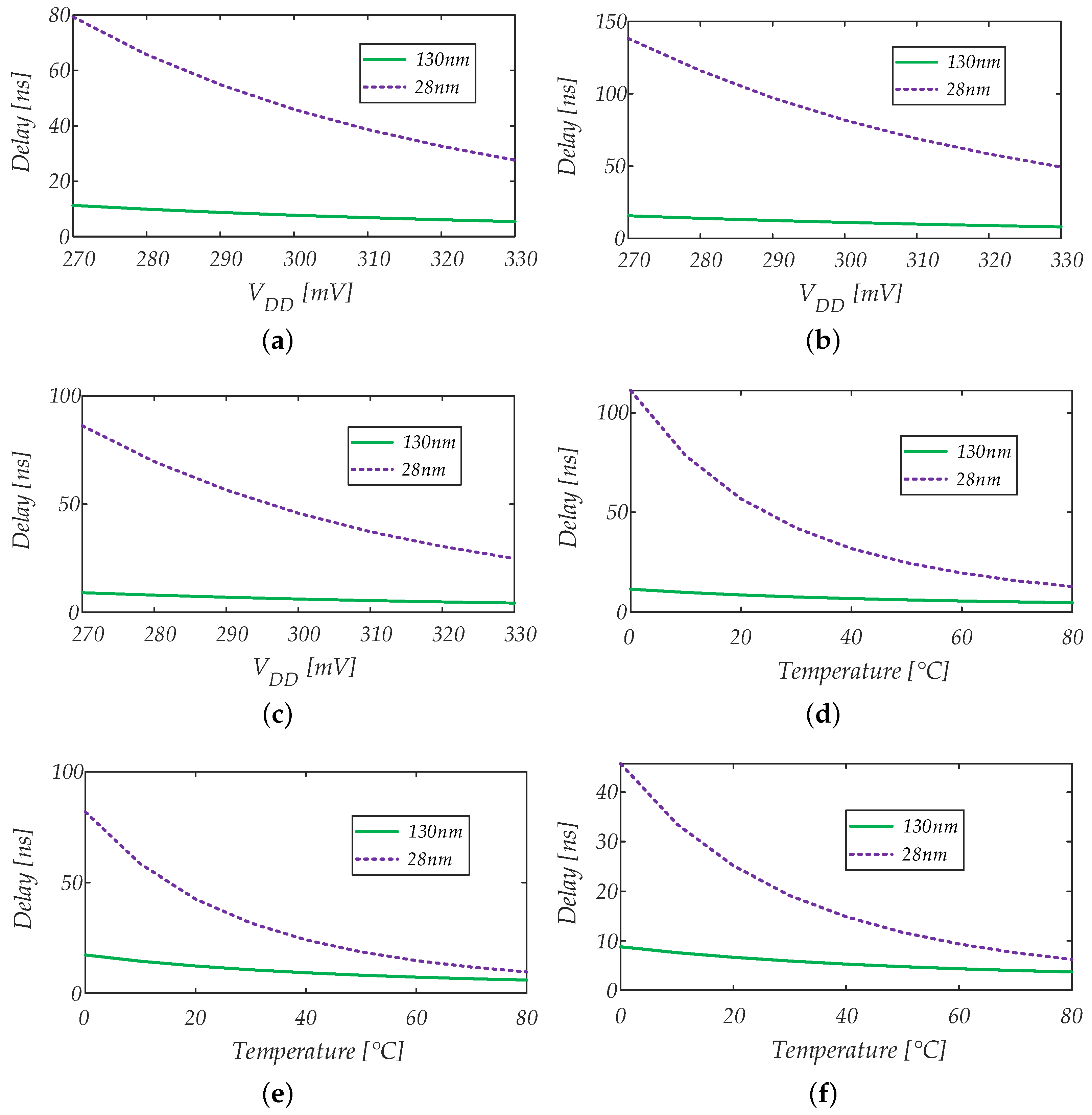
5.1.1. Propagation Delay

The propagation delay of the N A N D 3 -based comparator, measured according to Figure 1 as a function of the input common mode voltage, and considering a clock frequency of 10 Hz and an input differential signal of 10 mV, is reported in Figure 6a. It is evident from Figure 6a that the ICMR is not rail-to-rail; indeed, as expected, the comparator works fine for input common mode voltages V C M higher than V D D / 2 = 150 mV, whereas for V C M lower than 150 mV the delay starts to highly increase with respect to the nominal value. In fact, when the input common mode voltage is increased, the gate-source voltage of the NMOS transistor connected to the input signal (see Figure 3a) is lowered, and the current driving of the transistor is worsened. The abrupt rise in the propagation delay is due to the gate-source voltage of the NMOS transistor connected to the input signal to approach the threshold voltage of the device, thus drastically limiting its current drive capability.
The propagation delay as a function of the input differential signal amplitude for the N A N D 3 -based comparator is reported in Figure 6b for an input common mode voltage of 3 4 · V D D , which, for this comparator topology, is the mid-point of the ideal ICMR, and is therefore close to the V C M , at which delay is minimum. As can be observed, the propagation delay increases as the signal amplitude decreases, and the worst-case propagation delay occurs when the minimum differential input amplitude (1 mV) is considered.
The delay of the comparator as a function of the supply voltage and as a function of the temperature is reported in Figure 7a,b, respectively, showing the delay dependence on environmental conditions: propagation delay decreases at higher supply voltages and temperatures.
It is interesting to note that the propagation delay of the N A N D 3 -based comparator implemented in the 130 nm technology is faster than the N A N D 3 -based comparator implemented in the 28 nm technology. This is mainly due to the different threshold voltages of MOS devices in the two digital libraries adopted for the design. Considering the supply voltage of only 0.3 V since, for the 130 nm technology, low threshold voltage transistors are used, they are able to drive a higher current with respect to the high threshold voltage transistors adopted for the 28 nm library, resulting in faster operation. Obviously, this leads to higher power consumption of the comparator in 130 nm with respect to the comparator in 28 nm, as will be shown in the next section.

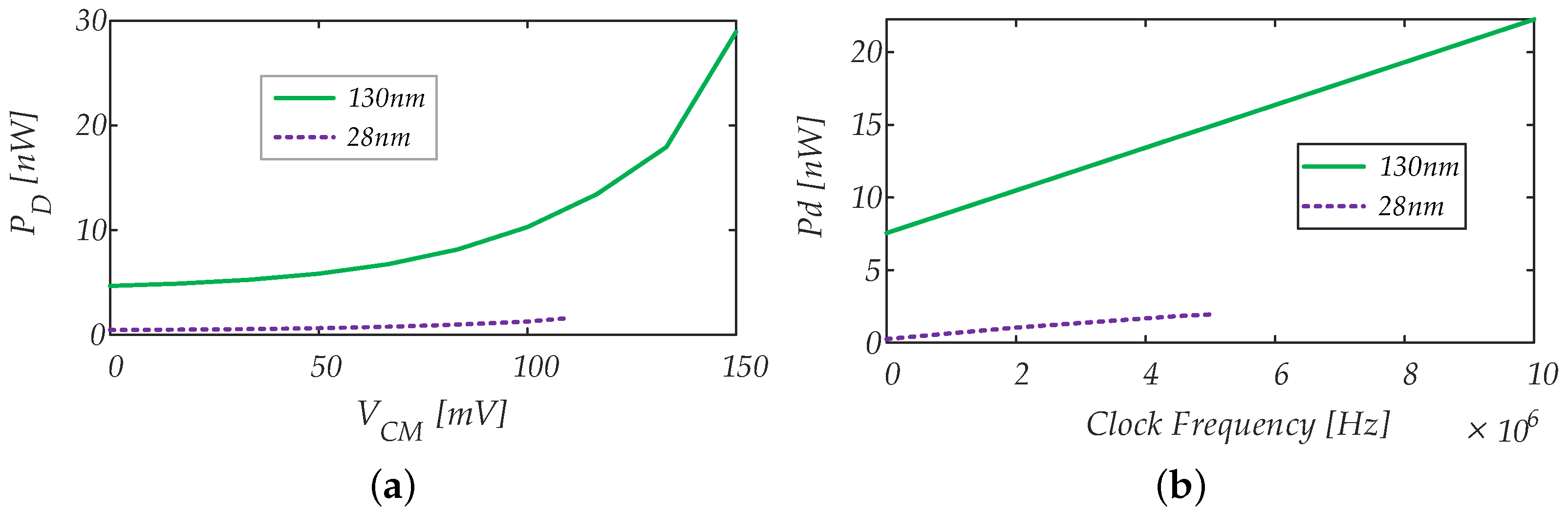
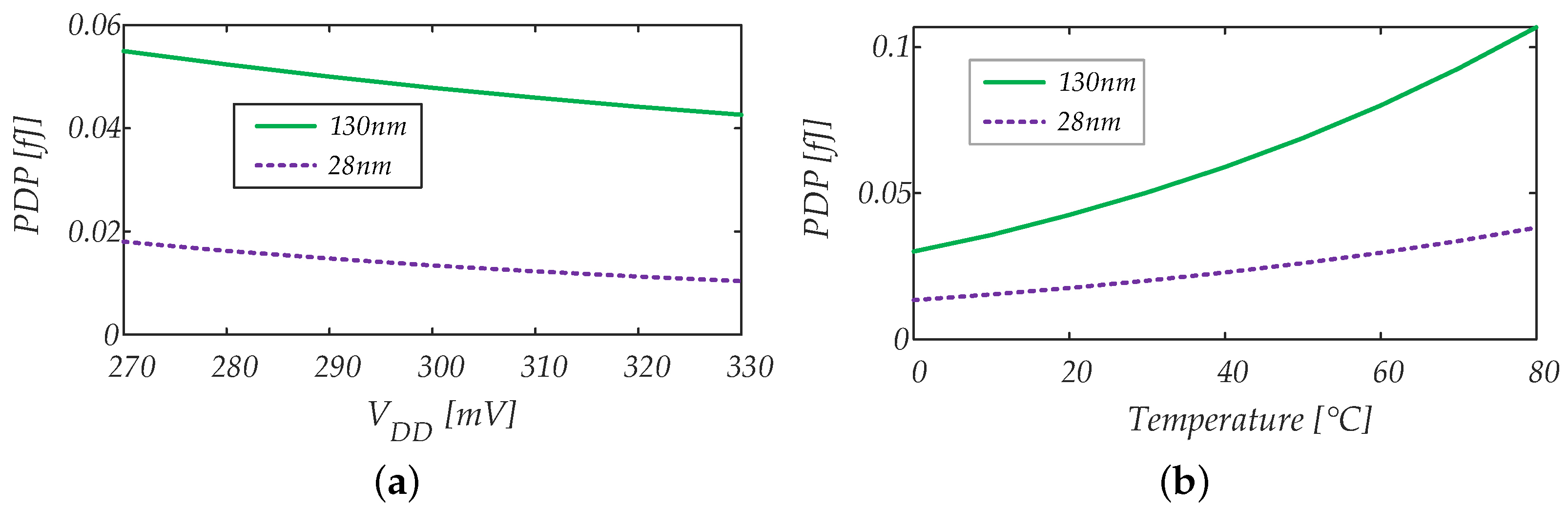
5.1.2. Power Consumption and Power–Delay Product

The power consumption versus the input common mode voltage of the N A N D 3 -based comparator measured at an operating frequency of 10 Hz is reported in Figure 8a, whereas Figure 8b shows the power dissipation of the N A N D 3 -based comparator as a function of the clock frequency for an input common mode voltage of 3 4 · V D D . Power consumption at 10 Hz is dominated by static power (which is particularly high for the 130 nm bulk CMOS technology) whereas, at higher frequencies, the dynamic power is the most relevant. In both figures, it is evident that power consumption in 28 nm is much lower than power consumption in 130 nm. This result was expected and is due to two main reasons:
  • The minimum-sized gates in 28 nm exhibit a much lower parasitic capacitance than the minimum-sized gates in 130 nm, thus resulting in much lower dynamic power;
  • The transistors of the considered 130 nm technology exhibit a lower threshold voltage compared to the transistors of the considered 28 nm FDSOI technology, and this results in deeper subthreshold operation for the 28 nm transistors at V D D = 0.3 V, resulting in much lower static power consumption for the 28 nm technology.
The Power–Delay Product (PDP) of the N A N D 3 -based comparator has been simulated under supply voltage and temperature variations, and the results are reported in Figure 9a,b, respectively. Of course, it is evident that the 28 nm technology allows the achieving a much lower PDP.

5.1.3. Offset

The input offset voltage of the N A N D 3 -based comparator has been evaluated considering an input common mode voltage equal to 3 4 · V D D . In order to account for the effect of mismatch, 1000 Monte Carlo simulations have been carried out, and results are reported for the 130 nm technology in Figure 10a and for the 28 nm technology in Figure 10b, showing that the input offset voltage can be described with a Gaussian distribution with mean value and standard deviation equal to μ 0.27 mV, σ 27.4 mV for the 130 nm technology, and μ 0.41 mV, σ 20.2 mV for the 28 nm technology.

5.2. N O R 3 -Based Comparator

This section reports the analysis and performance characterization of the comparator topology depicted in Figure 2b, proposed in [7] ( N O R 3 -based comparator).

5.2.1. Propagation Delay

The propagation delay as a function of the input common mode voltage for the N O R 3 -based comparator is reported in Figure 11a. It is evident from Figure 11a that the ICMR is not rail-to-rail; indeed, the N O R 3 -based comparator works fine for input common mode voltages V C M lower than V D D / 2 = 150 mV, as expected, whereas, for V C M approaching 150 mV, the delay results drastically increased with respect to the nominal value. In the case of the 28 nm technology, the ICMR is limited to a range from 0 to 110 mV.
The propagation delay as a function of the input differential signal amplitude for the N O R 3 -based comparator is reported in Figure 11b for an input common mode voltage of V D D / 4 . As can be observed, the delay increases when the differential input amplitude is lowered. At this purpose, it has to be pointed out that the N O R 3 -based comparator is not able to properly work for input differential signal amplitudes below 2.2 mV, and this is probably due to its lower gain with respect to the N A N D 3 -based comparator, where the input signal is further amplified by a N O T gate, which is not present in the N O R 3 -based comparator topology (see Figure 2b).
The delay of the comparator as a function of the supply voltage and as a function of the temperature is reported in Figure 12a,b, respectively, showing the delay dependence on environmental conditions. Furthermore, in this case, it is interesting to note that the propagation delay of the N O R 3 -based comparator implemented in the 130 nm technology is smaller than for the N O R r 3 -based comparator implemented in the 28 nm technology. This is mainly due to the different threshold voltages of MOS devices in the two digital libraries adopted for the design.

5.2.2. Power Consumption and Power–Delay Product

The power consumption versus the input common mode voltage of the N O R 3 -based comparator measured at an operating frequency of 10 Hz is reported in Figure 13a, whereas Figure 13b shows the power dissipation of the N O R 3 -based comparator as a function of the clock frequency for an input common mode voltage of V D D / 4 . The same considerations for the N A N D 3 -based comparator in terms of static and dynamic power components also apply in this case.
The Power–Delay Product (PDP) of the N O R 3 -based comparator has been simulated under supply voltage and temperature variations, and results are reported in Figure 14a,b, respectively.

5.2.3. Offset

The input offset voltage of the N O R 3 -based comparator has been evaluated considering an input common mode voltage equal to 1 4 · V D D . In order to consider the effect of the mismatch, 1000 Monte Carlo simulations have been carried out, and the results are reported for the 130 nm technology in Figure 15a and for the 28 nm technology in Figure 15b, showing that the input offset voltage can be described with a Gaussian distribution with mean value and standard deviation equal to μ 1.24 mV, σ 27.2 mV for the 130 nm technology, and μ 1.3 mV, σ 22.1 mV for the 28 nm technology.

5.3. Rail-to-Rail ICMR Standard-Cell Comparator

This section reports the analysis and performance characterization of the comparator topology depicted in Figure 4, proposed in [52,55] (rail-to-rail ICMR standard-cell comparator).

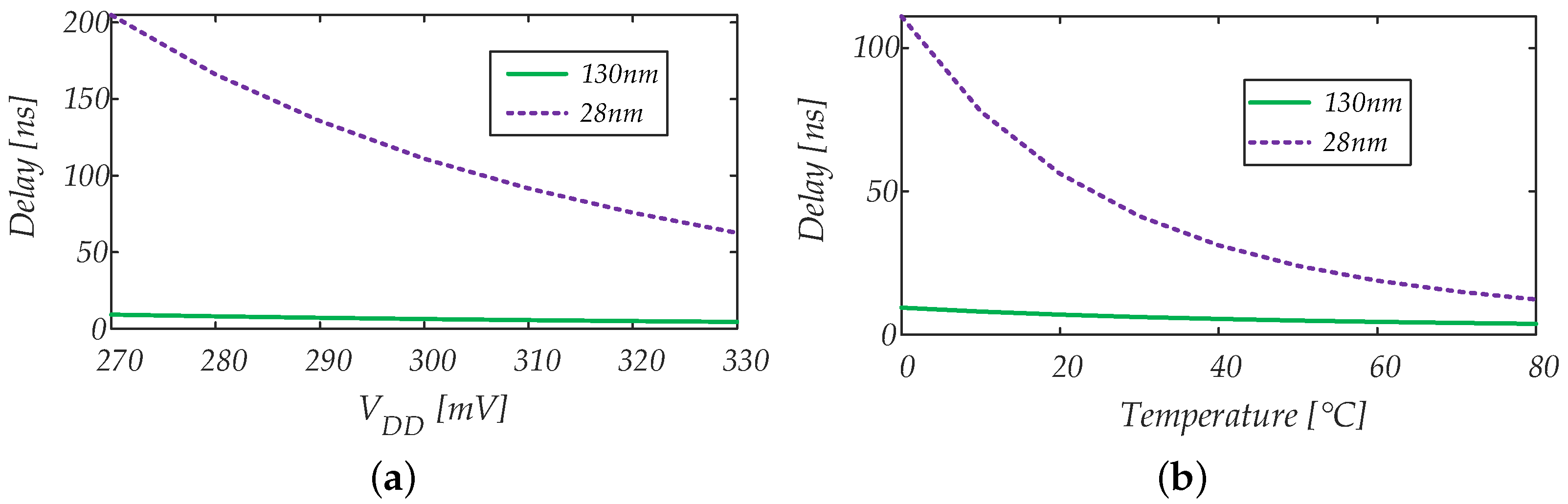
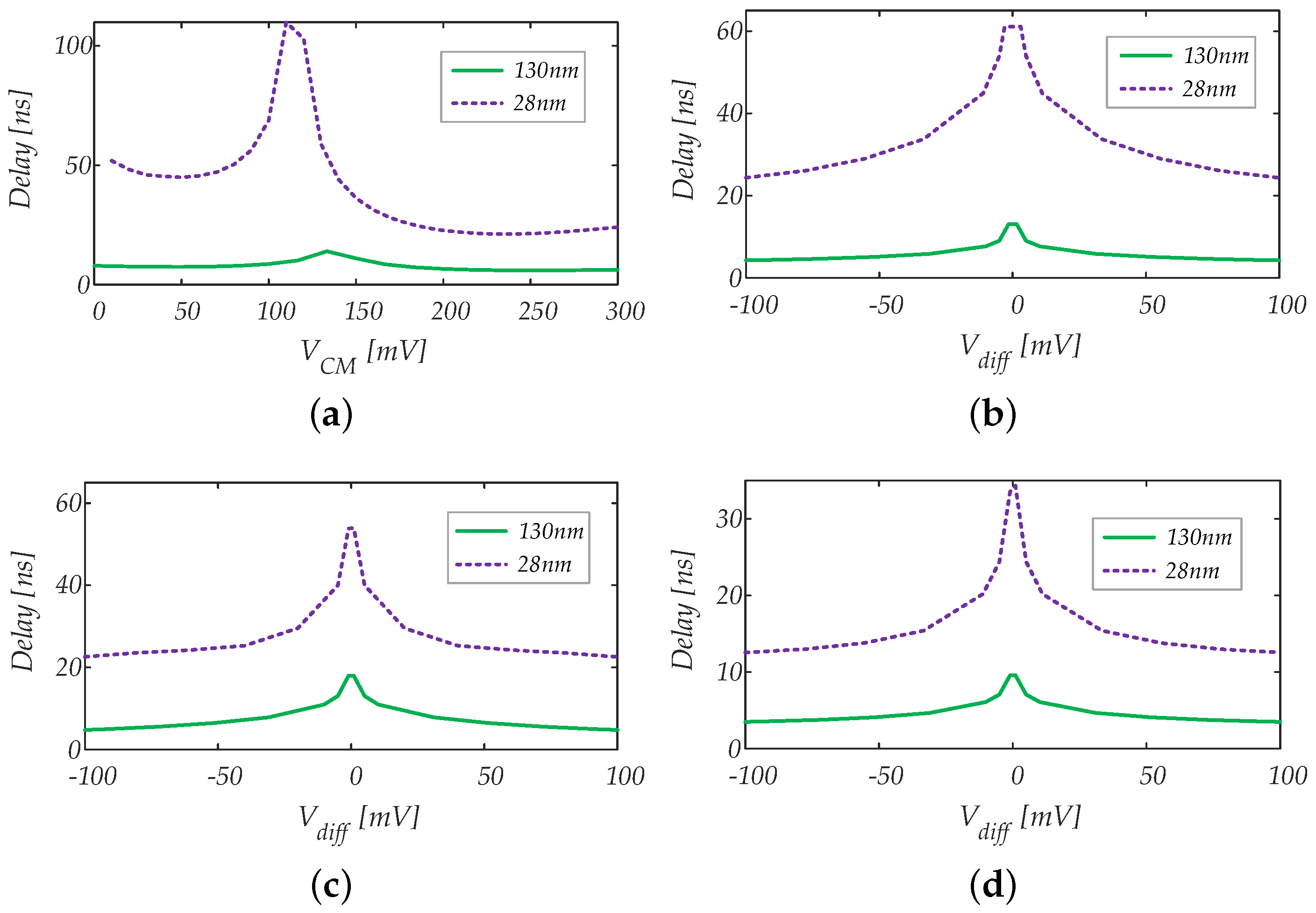
5.3.1. Propagation Delay

The propagation delay as a function of the input common mode voltage of the rail-to-rail ICMR standard-cell comparator is reported in Figure 16a. As can be observed, the maximum value of the propagation delay is obtained for an input common mode voltage of V D D / 2 , where both the N A N D 3 and N O R 3 cells are powered on. Indeed, for an input common mode voltage equal to V D D / 2 , both the N M O S and P M O S parts of both the N A N D 3 and N O R 3 cells (see the transistor level schematics in Figure 3a,b) are active and, thus, it is more difficult to unbalance the input differential cells.
The delay of the rail-to-rail comparator as a function of the input differential signal amplitude is reported in Figure 16b for an input common mode of V D D / 4 , in Figure 16c for an input common mode of V D D / 2 , and in Figure 16d for an input common mode of 3 / 4 · V D D . As can be observed, the worst case delay occurs when the minimum differential input voltage is considered.
The propagation delay of the rail-to-rail ICMR comparator as a function of the supply voltage is reported in Figure 17a for an input common mode of V D D / 4 , in Figure 17b for an input common mode of V D D / 2 , and in Figure 17c for an input common mode of 3 / 4 · V D D . The propagation delay of the rail-to-rail comparator as a function of the temperature is reported in Figure 17d for an input common mode of V D D / 4 , in Figure 17e for an input common mode of V D D / 2 , and in Figure 17f for an input common mode of 3 / 4 · V D D .

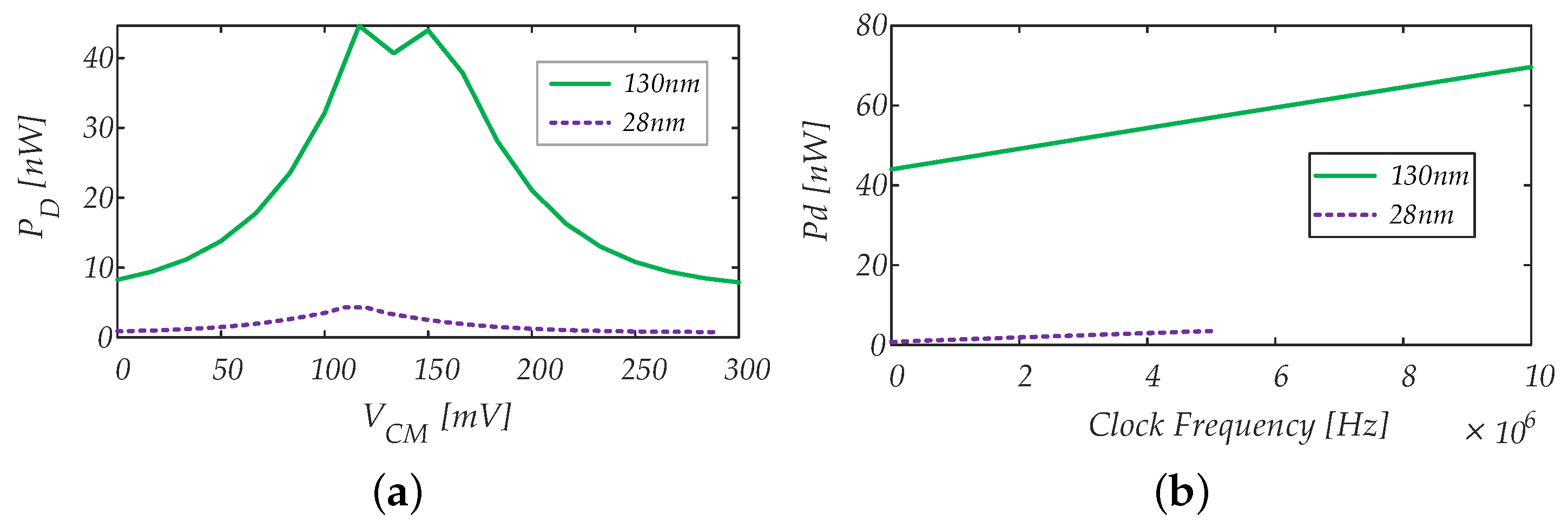
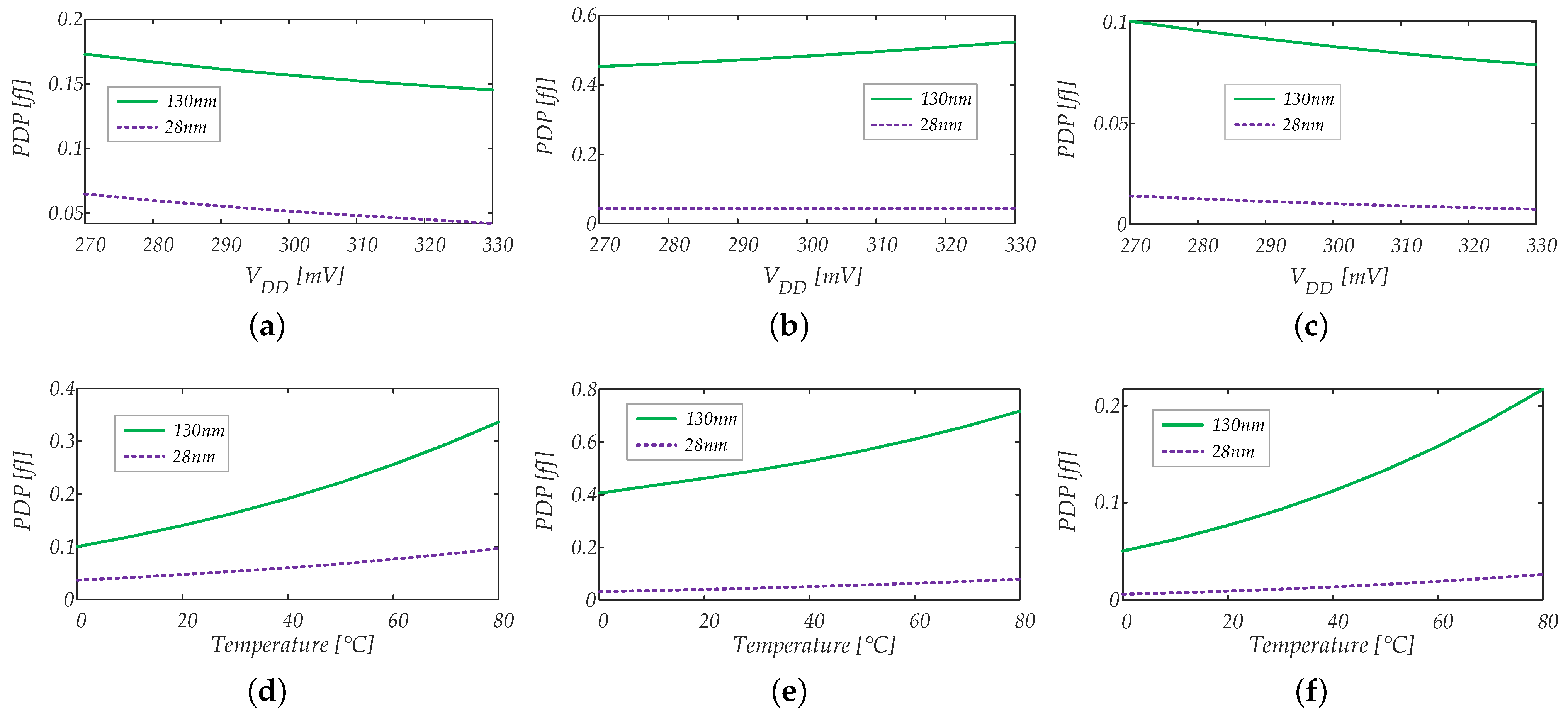
5.3.2. Power Consumption and Power–Delay Product
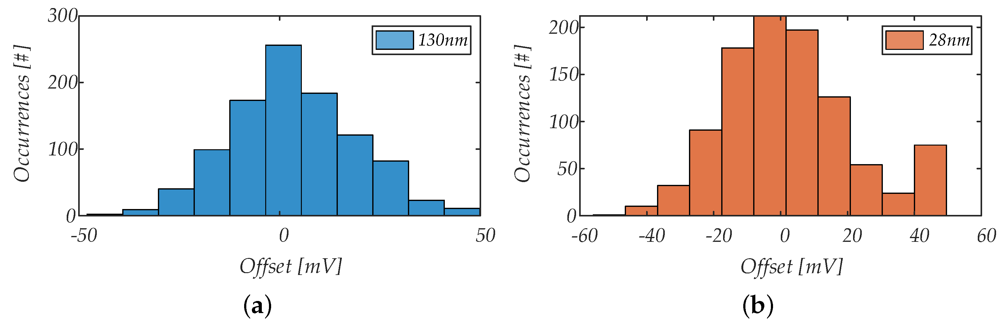
The power consumption versus the input common mode voltage of the rail-to-rail comparator measured at an operating frequency of 10 Hz is reported in Figure 18a, whereas Figure 18b shows the power dissipation of the rail-to-rail comparator as a function of the clock frequency for an input common mode voltage of V D D / 2 . The same considerations for the N A N D 3 and N O R 3 -based comparators in terms of static and dynamic power components apply also in this case. The power dissipation characteristic of the rail-to-rail comparator depicted in Figure 18b shows two “humps”, due to the two N A N D 3 and N O R 3 input cells, which are centered at two different input common mode voltages.
The Power–Delay Product of the rail-to-rail comparator as a function of the supply voltage is reported for an input common mode of V D D / 4 in Figure 19a, for an input common mode of V D D / 2 in Figure 19b, and for an input common mode of 3 / 4 · V D D in Figure 19c, whereas the Power–Delay Product of the rail-to-rail comparator as a function of the temperature for an input common mode of V D D / 4 is reported in Figure 19d, for an input common mode of V D D / 2 in Figure 19e, and for an input common mode of 3 / 4 · V D D in Figure 19f. As can be observed, the performance of the comparator is almost constant with respect to supply voltage variations, due to the fact that a higher power consumption corresponds to lower delays and, thus, the product between delay and power consumption is constant. Greater delay variations can be observed for temperature variations.

5.3.3. Offset

The input offset voltage of the rail-to-rail comparator has been evaluated considering an input common mode voltage equal to 1 2 · V D D . In order to consider the effect of mismatch, 1000 Monte Carlo simulations have been carried out, and the results are reported for the 130 nm technology in Figure 20a, and for the 28 nm technology in Figure 20b, showing that the input offset voltage can be described with a Gaussian distribution with mean value and standard deviation equal to μ 3.5 mV σ 15.5 mV, for the 130 nm technology, and μ 2.7 mV σ 19.9 mV, for the 28 nm technology.

6. Comparison

In this section, we compare the performances of the standard-cell-based latched comparator topologies described in Section 3 and calculate the figures of merit defined in Section 4.2. This allows us to draw conclusions on relative advantages and disadvantages, also taking into account the possible application scenarios.

6.1. Comparison in ULV Conditions

Comparisons are initially performed for a supply voltage of 0.3 V, since this is the typical context for the application of standard-cell-based analog circuits. Table 1 reports main performance parameters and FoMs both for the case of a high speed standard-cell library in a bulk 130 nm CMOS technology, and for the case of a high density, low leakage, standard-cell library in a 28 nm FDSOI CMOS technology. In the latter case, body bias is not exploited, thus larger delays are achieved due to the higher threshold voltage of the MOS devices. On the other hand, a much lower power consumption is achieved in 28 nm CMOS, due to the reduced speed and to a much lower static current, resulting in an overall better PDP performance.
For what concerns a comparison among the three tested topologies, Table 1 shows that the rail-to-rail topology presents the worst delay and power consumption for an input common mode voltage equal to V D D / 2 , where both the N A N D 3 and the N O R 3 parts are activated. For an input common mode voltage equal to V D D / 4 ( 3 4 · V D D ), the propagation delay is only slightly worse than for the N O R 3 ( N A N D 3 ) case, and power consumption is higher, especially for the 130 nm technology, where static power consumption is significant. The N A N D 3 topology performs better than the N O R 3 one, and the difference is very significant in the 28 nm technology. This is due to the fact that the absolute value of the threshold voltage of PMOS devices is higher than the threshold voltage of NMOS devices, and this is particularly evident in the 28 nm technology.
The input referred offset standard deviation is similar for all topologies, and ICMR is limited to half the supply voltage or less for the N A N D 3 and N O R 3 topologies.
Taking into account the results in Table 1, and the requirements of the different applications, a trade-off results between PDP and ICMR: if a large ICMR is nor required, the N A N D 3 and N O R 3 topologies are preferable, with the former providing better performance. Obviously, the rail-to-rail topology is required for a large (i.e., larger than V D D / 2 ) ICMR. If the application requires an input common mode equal to V D D / 2 , the N A N D 3 topology can be adopted, since it exhibits better performances than the rail-to-rail one. However, performances vs. the differential input voltage have to be examined, since, depending on technology, V D D / 2 can be at the edge of acceptable input common mode voltages.

6.2. Comparison at Higher Supply Voltages

A summary of the simulation results for the three considered standard-cell-based comparator topologies for different values of the supply voltage is reported in Table 2. Results in Table 2 confirm the trend observed at 0.3 V: the N A N D 3 topology is the fastest one, when operated for an input common mode voltage of 3 4 · V D D , but its ICMR is limited to about half the supply voltage. The N O R 3 topology is slightly slower, and exhibits an ICMR which is about half the supply voltage for all the considered values of V D D . The rail-to-rail topology provides a rail-to-rail ICMR, but with higher delay and power consumption at all the considered input common mode voltages, exhibiting the worst case performances at V C M = V D D / 2 .
Results in Table 2 also show that the performances of all the standard-cell-based comparators considered in this work scale with the supply voltage, thus allowing optimization of the trade off between speed and power consumption in different operating conditions through V D D adjusting.

7. Conclusions

In this paper, we have simulated and compared three different standard-cell-based comparator topologies in ULV conditions. In order to better compare comparator performances in different application scenarios, we have introduced a set of FoMs. The simulation testbenches and conditions have been explained in detail, and used to simulate the considered topologies referring to two different technologies: a conventional 130 nm bulk CMOS process and a 28 nm FDSOI CMOS technology. Simulation results have shown that the performances of the different comparators are strongly dependent on the input common voltage. The ICMR of the N A N D 3 -based comparator has been found to be about from V D D / 2 to V D D , whereas the ICMR of the N o r 3 -based comparator has been found to be about from 0 to V D D / 2 ; thus, neither of these comparator topologies exhibit a rail-to-rail ICMR. We have also found that the propagation delay of these comparators has its minimum value for an input common mode voltage close to the midpoint of the input ICMR (i.e., 3 V D D / 4 for the N A N D 3 and V D D / 4 for the N O R 3 -based comparator, respectively). The rail-to-rail standard-cell-based comparator considered in this work exhibits two minima for the propagation delay as a function of the input common mode voltage, which are at about V D D / 4 and 3 V D D / 4 , whereas for an input common mode voltage equal to V D D / 2 , this comparator exhibits its worst case performance. We have also analyzed how the performances of the considered comparator topologies scale with the supply voltage, and simulation results have shown that, even if standard-cell-based comparators can be used at higher supply voltages, the best values of the FoMs are achieved at ULV conditions.

Author Contributions

Conceptualization, F.C., R.D.S. and G.S.; data curation, R.D.S.; investigation, F.C., R.D.S., G.P. and G.S.; software, R.D.S. and F.C.; validation, G.P.; supervision, G.S. and G.P.; writing—original draft preparation, R.D.S. and G.S.; writing—review and editing, G.S. and G.P. All authors have read and agreed to the published version of the manuscript.

Funding

This research received no external funding.

Institutional Review Board Statement

Not applicable.

Informed Consent Statement

Not applicable.

Conflicts of Interest

The authors declare no conflict of interest.

References

  1. Sumanen, L.; Waltari, M.; Halonen, K.A.I. A 10-bit 200-MS/s CMOS parallel pipeline A/D converter. IEEE J. Solid-State Circuits 2001, 36, 1048–1055. [Google Scholar] [CrossRef]
  2. Lin, J.; Haroun, B. An embedded 0.8 V/480 /spl mu/W 6b/22 MHz flash ADC in 0.13-/spl mu/m digital CMOS process using a nonlinear double interpolation technique. IEEE J. Solid-State Circuits 2002, 37, 1610–1617. [Google Scholar] [CrossRef]
  3. Fahmy, A.; Liu, J.; Kim, T.; Maghari, N. An all-digital scalable and reconfigurable wide-input range stochastic ADC using only standard cells. IEEE Trans. Circuits Syst. II 2015, 62, 731–735. [Google Scholar] [CrossRef]
  4. Kadayinti, N.; Sharma, D.K. Sense amplifier comparator with offset correction for decision feedback equalization based receivers. Microelectron. J. 2017, 70, 27–33. [Google Scholar] [CrossRef]
  5. Gandhi, P.P.; Devashrayee, N.M. A novel low offset low power CMOS dynamic comparator. Analog. Integr. Circ. Sig. Process. 2018, 96, 147–158. [Google Scholar] [CrossRef]
  6. Xu, Z.; Ojima, N.; Li, S.; Iizuka, T. An all-standard-cell-based synthesizable SAR ADC with nonlinearity-compensated RDAC. IEEE Trans. Very Large Scale Integr. VLSI Syst. 2021, 29, 2153–2162. [Google Scholar] [CrossRef]
  7. Weaver, S.; Hershberg, B.; Moon, U.K. Digitally synthesized stochastic flash ADC using only standard digital cells. IEEE Trans. Circ. Syst. I 2014, 61, 84–91. [Google Scholar] [CrossRef]
  8. Seo, M.J.; Roh, Y.J.; Chang, D.J.; Kim, W.; Kim, Y.D.; Ryu, S.T. A reusable code-based SAR ADC design with CDAC compiler and synthesizable analog building blocks. IEEE Trans. Circuits Syst. II 2018, 65, 1904–1908. [Google Scholar] [CrossRef]
  9. Park, J.E.; Hwang, Y.H.; Jeong, D.K. A 0.5-V fully synthesizable SAR ADC for on-chip distributed waveform monitors. IEEE Access 2019, 7, 63686–63697. [Google Scholar] [CrossRef]
  10. Sood, L.; Agarwal, A. A CMOS standard-cell based fully-synthesizable low-dropout regulator for ultra-low power applications. AEU Int. J. Electron. Commun. 2021, 141, 153958. [Google Scholar] [CrossRef]
  11. Wang, D.; Wang, Z.; Xu, H.; Wang, J.; Zhao, Z.; Zhang, C.; Wang, Z.; Chen, H. A 56-Gbps PAM-4 wireline receiver with 4-tap direct DFE employing dynamic CML comparators in 65 nm CMOS. IEEE Trans. Circ. Syst. I 2022, 69, 1027–1040. [Google Scholar] [CrossRef]
  12. Kobayashi, T.; Nogami, K.; Shirotori, T.; Fujimoto, Y.; Watanabe, O. A current-mode latch sense amplifier and a static power saving input buffer for low-power architecture. In Proceedings of the 1992 Symposium on VLSI Circuits, Seattle, WA, USA, 4–6 June 1992; IEEE: Piscataway, NJ, USA, 1992; pp. 28–29. [Google Scholar] [CrossRef]
  13. Montiel-Nelson, J.A.; Navarro, V.; Sosa, J.; Bautista, T. Analysis and optimization of dynamically reconfigurable regenerative comparators for ultra-low power 6-bit TC-ADCs in 90nm CMOS technologies. Microelectron. J. 2014, 45, 1247–1253. [Google Scholar] [CrossRef]
  14. Razavi, B. The StrongARM latch. IEEE Solid-State Circuits Mag. 2015, 7, 12–17. [Google Scholar] [CrossRef]
  15. Schinkel, D.; Mensink, E.; Klumperink, E.; van Tuijl, E.; Nauta, B. A double-tail latch-type voltage sense amplifier with 18ps setup+hold time. In Proceedings of the 2007 IEEE International Solid-State Circuits Conference (ISSCC), San Francisco, CA, USA, 11–15 February 2007; IEEE: Piscataway, NJ, USA, 2007; pp. 314–605. [Google Scholar] [CrossRef]
  16. Babayan-Mashhadi, S.; Lotfi, R. Analysis and design of a low-voltage low-power double-tail comparator. IEEE Trans. Very Large Scale Integr. VLSI Syst. 2014, 22, 343–352. [Google Scholar] [CrossRef]
  17. Khorami, A.; Sharifkhani, M. A low-power high-speed comparator for precise applications. IEEE Trans. Very Large Scale Integr. VLSI Syst. 2018, 26, 2038–2049. [Google Scholar] [CrossRef]
  18. Chevella, S.; O’Hare, D.; O’Connell, I. A Low-Power 1-V supply dynamic comparator. IEEE Solid-State Circuits Lett. 2020, 3, 154–157. [Google Scholar] [CrossRef]
  19. Mehr, I.; Dalton, D. A 500-MSample/s, 6-bit Nyquist-rate ADC for disk-drive read-channel applications. IEEE J. Solid-State Circuits 1999, 34, 912–920. [Google Scholar] [CrossRef]
  20. Usama, M.; Kwasniewski, T. Design and comparison of CMOS Current Mode Logic latches. In Proceedings of the 2004 IEEE International Symposium on Circuits and Systems (ISCAS), Vancouver, BC, Canada, 23–26 May 2004; IEEE: Piscataway, NJ, USA, 2004; Volume 4, pp. 353–356. [Google Scholar] [CrossRef]
  21. Goll, B.; Zimmermann, H. Low-power 600 MHz comparator for 0.5 V supply voltage in 0.12 μm CMOS. Electron. Lett. 2007, 43, 388–390. [Google Scholar] [CrossRef]
  22. Mohtashemi, D.; Green, M.M. A low-power 8-GS/s comparator for high-speed analog-to-digital conversion in 0.13 μm CMOS technology. IEEE Trans. Circuits Syst. II 2019, 66, 557–561. [Google Scholar] [CrossRef]
  23. Martins, R.; Lourenco, N.; Horta, N. LAYGEN II- Automatic layout generation of analog integrated circuits. IEEE Trans. Comput. Aided Des. Integr. Circuits Syst. 2013, 32, 1641–1654. [Google Scholar] [CrossRef]
  24. Martins, R.; Lourenço, N.; Canelas, A.; Póvoa, R.; Horta, N. AIDA: Robust layout-aware synthesis of analog ICs including sizing and layout generation. In Proceedings of the 2015 International Conference on Synthesis, Modeling, Analysis and Simulation Methods and Applications to Circuit Design (SMACD), Istanbul, Turkey, 7–9 September 2014; IEEE: Piscataway, NJ, USA, 2015; pp. 1–4. [Google Scholar] [CrossRef]
  25. Maji, K.B.; Kar, R.; Mandal, D.; Ghoshal, S.P. An evolutionary approach based design automation of low power CMOS Two-Stage Comparator and Folded Cascode OTA. AEU Int. J. Electron. Commun. 2016, 70, 398–408. [Google Scholar] [CrossRef]
  26. Bashir, M.; Abbassi, F.; Misic, M.V.; Sturm, J.; Getnot, H. Performance comparison of BAG and custom generated analog layout for single-tail dynamic comparator. In Proceedings of the 2020 Austrochip Workshop on Microelectronics (Austrochip), Vienna, Austria, 7 October 2020; IEEE: Piscataway, NJ, USA, 2020; pp. 37–41. [Google Scholar] [CrossRef]
  27. Settaluri, K.; Liu, Z.; Khurana, R.; Mirhaj, A.; Jain, R.; Nikolic, B. Automated design of analog circuits using reinforcement learning. IEEE Trans. Comput. Aided Des. Integr. Circuits Syst. 2022, 41, 2794–2807. [Google Scholar] [CrossRef]
  28. Patyal, A.; Chen, H.M.; Lin, M.P.H.; Fang, G.Q.; Chen, S.Y.H. Pole-aware analog layout synthesis considering monotonic current flows and wire crossings. IEEE Trans. Comput. Aided Des. Integr. Circuits Syst. 2022, 42, 266–279. [Google Scholar] [CrossRef]
  29. Newton, S.M.; Kinget, P.R. A 4th-order analog continuous-time filter designed using standard cells and automatic digital logic design tools. In Proceedings of the 2016 IEEE International Symposium on Circuits and Systems (ISCAS), Montreal, QC, Canada, 22–25 May 2016; IEEE: Piscataway, NJ, USA, 2016; pp. 297–300. [Google Scholar] [CrossRef]
  30. Liu, J.; Park, B.; Guzman, M.; Fahmy, A.; Kim, T.; Maghari, N. A fully synthesized 77-dB SFDR reprogrammable SRMC filter using digital standard cells. IEEE Trans. Very Large Scale Integr. VLSI Syst. 2018, 26, 1126–1138. [Google Scholar] [CrossRef]
  31. Liu, Y.; Zhang, B.; Cheng, X.; Han, J.; Zeng, X. A 0.9V all digital synthesizable OPAMP with boosted gain and widened common mode input range. In Proceedings of the 2020 IEEE 15th International Conference on Solid-State & Integrated Circuit Technology (ICSICT), Kunming, China, 3–6 November 2020; IEEE: Piscataway, NJ, USA, 2020; pp. 1–3. [Google Scholar] [CrossRef]
  32. Centurelli, F.; Giustolisi, G.; Pennisi, S.; Scotti, G. A biasing approach to design ultra-low-power standard-cell-based analog building blocks for nanometer SoCs. IEEE Access 2022, 10, 25892–25900. [Google Scholar] [CrossRef]
  33. Centurelli, F.; Della Sala, R.; Scotti, G. A standard-cell-based CMFB for fully synthesizable OTAs. J. Low Power Electron. Appl. 2022, 12, 27. [Google Scholar] [CrossRef]
  34. Della Sala, R.; Centurelli, F.; Scotti, G. Enabling ULV fully synthesizable analog circuits: The BA cell, a standard-cell-based building block for analog design. IEEE Trans. Circuits Syst. II 2022, 69, 4689–4693. [Google Scholar] [CrossRef]
  35. Toledo, P.; Rubino, R.; Musolino, F.; Crovetti, P. Re-thinking analog integrated circuits in digital terms: A new design concept for the IoT era. IEEE Trans. Circuits Syst. II 2021, 68, 816–822. [Google Scholar] [CrossRef]
  36. Crovetti, P.S. A digital-based analog differential circuit. IEEE Trans. Circ. Syst. I 2013, 60, 3107–3116. [Google Scholar] [CrossRef]
  37. Toledo, P.; Crovetti, P.; Aiello, O.; Alioto, M. Design of digital OTAs with operation down to 0.3 V and nW power for direct harvesting. IEEE Trans. Circ. Syst. I 2021, 68, 3693–3706. [Google Scholar] [CrossRef]
  38. Palumbo, G.; Scotti, G. A novel standard-cell-based implementation of the digital OTA suitable for automatic place and route. J. Low Power Electron. Appl. 2021, 11, 42. [Google Scholar] [CrossRef]
  39. Unnikrishnan, V.; Vesterbacka, M. Time-mode analog-to-digital conversion using standard cells. IEEE Trans. Circ. Syst. I 2014, 61, 3348–3357. [Google Scholar] [CrossRef]
  40. Ojima, N.; Xu, Z.; Iizuka, T. A 0.0053-mm2 6-bit fully-standard-cell-based synthesizable SAR ADC in 65 nm CMOS. In Proceedings of the 2019 17th IEEE International New Circuits and Systems Conference (NEWCAS), Munich, Germany, 23–26 June 2019; IEEE: Piscataway, NJ, USA, 2019; pp. 1–4. [Google Scholar] [CrossRef]
  41. Aiello, O.; Crovetti, P.; Alioto, M. Fully synthesizable low-area analogue-to-digital converters with minimal design effort based on the dyadic digital pulse modulation. IEEE Access 2020, 8, 70890–70899. [Google Scholar] [CrossRef]
  42. Aiello, O.; Crovetti, P.S.; Alioto, M. Fully synthesizable low-area digital-to-analog converter with graceful degradation and dynamic power-resolution scaling. IEEE Trans. Circ. Syst. I 2019, 66, 2865–2875. [Google Scholar] [CrossRef]
  43. Aiello, O.; Crovetti, P.; Alioto, M. Standard cell-based ultra-compact DACs in 40-nm CMOS. IEEE Access 2019, 7, 126479–126488. [Google Scholar] [CrossRef]
  44. Park, Y.; Wentzloff, D.D. An all-digital PLL synthesized from a digital standard cell library in 65nm CMOS. In Proceedings of the 2011 IEEE Custom Integrated Circuits Conference (CICC), San Jose, CA, USA, 19–21 September 2011; IEEE: Piscataway, NJ, USA, 2011; pp. 1–4. [Google Scholar] [CrossRef]
  45. Deng, W.; Yang, D.; Ueno, T.; Siriburanon, T.; Kondo, S.; Okada, K.; Matsuzawa, A. A fully synthesizable all-digital PLL with interpolative phase coupled oscillator, current-output DAC, and fine-resolution digital varactor using gated edge injection technique. IEEE J. Solid-State Circuits 2015, 50, 68–80. [Google Scholar] [CrossRef]
  46. Liu, J.; Maghari, N. A fully-synthesizable 0.6 V digital LDO with dual-loop control using digital standard cells. In Proceedings of the 2016 14th IEEE International New Circuits and Systems Conference (NEWCAS), Vancouver, BC, Canada, 26–29 June 2016; IEEE: Piscataway, NJ, USA, 2016; pp. 1–4. [Google Scholar] [CrossRef]
  47. Akram, M.A.; Hong, W.; Hwang, I.C. Fast transient fully standard-cell-based all digital low-dropout regulator with 99.97% current efficiency. IEEE Trans. Power Electron. 2018, 33, 8011–8019. [Google Scholar] [CrossRef]
  48. Ojima, N.; Nakura, T.; Iizuka, T.; Asada, K. A synthesizable digital low-dropout regulator based on voltage-to-time conversion. In Proceedings of the 2018 IFIP/IEEE International Conference on Very Large Scale Integration (VLSI-SoC), Verona, Italy, 8–10 October 2018; IEEE: Piscataway, NJ, USA, 2018; pp. 55–58. [Google Scholar] [CrossRef]
  49. Sood, L.; Agarwal, A. A transient-enhanced low-power standard-cell-based digital LDO. Arab. J. Sci. Eng. 2022, 47, 13943–13953. [Google Scholar] [CrossRef]
  50. Xu, B.; Li, S.; Sun, N.; Pan, D.Z. A scaling compatible, synthesis friendly VCO-based delta-sigma ADC design and synthesis methodology. In Proceedings of the 2017 54th ACM/EDAC/IEEE Design Automation Conference (DAC), Austin, TX, USA, 18–22 June 2017; IEEE: Piscataway, NJ, USA, 2017; pp. 1–6. [Google Scholar] [CrossRef]
  51. Li, S.; Xu, B.; Pan, D.Z.; Sun, N. A 60-fJ/step 11-ENOB VCO-based CTDSM synthesized from digital standard cell library. In Proceedings of the 2019 IEEE Custom Integrated Circuits Conference (CICC), Austin, TX, USA, 14–17 April 2019; IEEE: Piscataway, NJ, USA, 2019; pp. 1–4. [Google Scholar] [CrossRef]
  52. Aiello, O.; Crovetti, P.; Alioto, M. Fully synthesizable, rail-to-rail dynamic voltage comparator for operation down to 0.3 V. In Proceedings of the 2018 IEEE International Symposium on Circuits and Systems (ISCAS), Florence, Italy, 27–30 May 2018; IEEE: Piscataway, NJ, USA, 2018; pp. 1–5. [Google Scholar] [CrossRef]
  53. Li, X.; Zhou, T.; Ji, Y.; Li, Y. A 0.35 V-to-1.0 V synthesizable rail-to-rail dynamic voltage comparator based OAI&AOI logic. Analog. Integr.Circ. Sig. Process. 2020, 104, 351–357. [Google Scholar] [CrossRef]
  54. Aiello, O.; Toledo, P. Temperature characterization of a fully-synthesizable rail-to-rail dynamic voltage comparator operating down to 0.15-V. In Proceedings of the 2021 19th IEEE International New Circuits and Systems Conference (NEWCAS), Toulon, France, 13–16 June 2021; IEEE: Piscataway, NJ, USA, 2021; pp. 1–4. [Google Scholar] [CrossRef]
  55. Aiello, O.; Crovetti, P.; Toledo, P.; Alioto, M. Rail-to-rail dynamic voltage comparator scalable down to pW-range power and 0.15-V supply. IEEE Trans. Circuits Syst. II 2021, 68, 2675–2679. [Google Scholar] [CrossRef]
  56. Zhou, T.; Li, X.; Ji, Y.; Li, Y. A 0.25-1.0 V fully synthesizable three-stage dynamic voltage comparator based XOR & XNOR & NAND & NOR logic. Analog. Integr.Circ. Sig. Process. 2021, 108, 221–228. [Google Scholar] [CrossRef]
  57. Li, M.; Wang, J.; Cheng, X.; Zeng, X. A fully synthesizable dynamic latched comparator with reduced kickback noise. In Proceedings of the 2022 IEEE International Symposium on Circuits and Systems (ISCAS), Austin, TX, USA, 27 May–1 June 2022; IEEE: Piscataway, NJ, USA, 2022; pp. 2876–2880. [Google Scholar] [CrossRef]
  58. Wicht, B.; Nirschl, T.; Schmitt-Landsiedel, D. Yield and speed optimization of a latch-type voltage sense amplifier. IEEE J. Solid-State Circuits 2004, 39, 1148–1158. [Google Scholar] [CrossRef]
  59. Savani, V.; Devashrayee, N.M. Analysis of power for double-tail current dynamic latch comparator. Analog. Integr.Circ. Sig. Process. 2019, 100, 345–355. [Google Scholar] [CrossRef]
  60. Xu, H.; Abidi, A.A. Analysis and design of regenerative comparators for low offset and noise. IEEE Trans. Circ. Syst. I 2019, 66, 2817–2830. [Google Scholar] [CrossRef]
  61. Pelgrom, M.J.M. Comparators. In Analog-to-Digital Conversion; Springer: Cham, Switzerland, 2021; pp. 599–641. [Google Scholar] [CrossRef]
  62. Veendrick, H.J.M. The behaviour of flip-flops used as synchronizers and prediction of their failure rate. IEEE J. Solid-State Circuits 1980, 15, 169–176. [Google Scholar] [CrossRef]
  63. Juan-Chico, J.; Bellido, M.J.; Acosta, A.J.; Valencia, M.; Huertas, J.L. Analysis of metastable operation in a CMOS dynamic D-latch. Analog. Integr. Circuits Signal Process. 1997, 14, 143–157. [Google Scholar] [CrossRef]
  64. Figueiredo, P.M. Comparator metastability in the presence of noise. IEEE Trans. Circ. Syst. I 2013, 60, 1286–1299. [Google Scholar] [CrossRef]
  65. Razavi, B. The design of a comparator. IEEE Solid-State Circuits Mag. 2020, 12, 8–14. [Google Scholar] [CrossRef]
  66. He, J.; Zhan, S.; Chen, D.; Geiger, R.L. Analyses of static and dynamic random offset voltages in dynamic comparators. IEEE Trans. Circ. Syst. I 2009, 56, 911–919. [Google Scholar] [CrossRef]
  67. Nuzzo, P.; De Bernardinis, F.; Terreni, P.; Van der Plas, G. Noise analysis of regenerative comparators for reconfigurable ADC architectures. IEEE Trans. Circ. Syst. I 2008, 55, 1441–1454. [Google Scholar] [CrossRef]
  68. Kim, J.; Leibowitz, B.S.; Ren, J.; Madden, C.J. Simulation and analysis of random decision errors in clocked comparators. IEEE Trans. Circ. Syst. I 2009, 56, 1844–1857. [Google Scholar] [CrossRef]
  69. Lei, K.M.; Mak, P.I.; Martins, R.P. Systematic analysis and cancellation of kickback noise in a dynamic latched comparator. Analog. Integr.Circ. Sig. Process. 2013, 77, 277–284. [Google Scholar] [CrossRef]
  70. Sundstrom, T.; Alvandpour, A. Utilizing process variations for reference generation in a flash ADC. IEEE Trans. Circuits Syst. II 2009, 56, 364–368. [Google Scholar] [CrossRef]
  71. Weaver, S.; Hershberg, B.; Kurahashi, P.; Knierim, D.; Moon, U.K. Stochastic flash analog-to-digital conversion. IEEE Trans. Circ. Syst. I 2010, 57, 2825–2833. [Google Scholar] [CrossRef]
  72. Jeon, M.K.; Yoo, W.J.; Kim, C.G.; Yoo, C. A stochastic flash analog-to-digital converter linearized by reference swapping. IEEE Access 2017, 5, 23046–23051. [Google Scholar] [CrossRef]
  73. Liu, C.C.; Chang, S.J.; Huang, G.Y.; Lin, Y.Z. A 10-bit 50-MS/s SAR ADC with a monotonic capacitor switching procedure. IEEE J. Solid-State Circuits 2010, 45, 731–740. [Google Scholar] [CrossRef]
  74. Urkin, T.; Abramov, E.; Peretz, M.M. Enhanced performance fully-synthesizable ∑Δ ADC for efficient digital voltage-mode control. In Proceedings of the 2018 IEEE 19th Workshop on Control and Modeling for Power Electronics (COMPEL), Padua, Italy, 25–28 June 2018; IEEE: Piscataway, NJ, USA, 2018; pp. 1–8. [Google Scholar] [CrossRef]
  75. Della Sala, R.; Centurelli, F.; Monsurrò, P.; Scotti, G.; Trifiletti, A. A 0.3 V Rail-to-Rail Three-Stage OTA with High DC Gain and Improved Robustness to PVT Variations. IEEE Access 2023, 11, 19635–19644. [Google Scholar] [CrossRef]
  76. Kulej, T.; Khateb, F. A 0.3-V 98-dB Rail-to-Rail OTA in 0.18 μm CMOS. IEEE Access 2020, 8, 27459–27467. [Google Scholar] [CrossRef]
  77. Kulej, T.; Khateb, F.; Kumngern, M. 0.3-V nanopower biopotential low-pass filter. IEEE Access 2020, 8, 119586–119593. [Google Scholar] [CrossRef]
Figure 1. Comparator time-related parameters.
Chips 02 00011 g001
Figure 2. Comparators presented in [7] with N A N D logic gates (a) and N O R gates (b).
Chips 02 00011 g002
Figure 3. Schematic of logic cells N A N D 3 (a) and N O R 3 (b).
Chips 02 00011 g003
Figure 4. Comparator presented in [52,55].
Chips 02 00011 g004
Figure 5. Layout screenshots for the rail-to-rail topology implemented in the 130 nm technology with an area of 9.84 × 7.79 μ m 2 (a), and implemented in the 28 nm technology with an area of 2.4 × 1.5 μ m 2 (b).
Chips 02 00011 g005
Figure 6. Propagation delay of the N A N D 3 -based comparator as a function of the input common mode voltage (a) and input differential signal amplitude (b).
Chips 02 00011 g006
Figure 7. Propagation delay of the N A N D 3 -based comparator with respect to supply voltage variations (a) and temperature variations (b).
Chips 02 00011 g007
Figure 8. Power dissipation of the N A N D 3 -based comparator as a function of the input common mode voltage measured @ 10 Hz (a), and power dissipation of the N A N D 3 -based comparator as a function of the clock frequency for an input common mode voltage of 3 4 · V D D (b).
Chips 02 00011 g008
Figure 9. Power–Delay Product (PDP) of the N A N D 3 -based comparator with respect to supply voltage variations (a) and temperature variations (b).
Chips 02 00011 g009
Figure 10. Input offset voltage of the N A N D 3 -based comparator evaluated by using 1000 mismatch Monte Carlo simulations for the 130 nm technology (a) and for the 28 nm technology (b).
Chips 02 00011 g010
Figure 11. Propagation delay of the N O R 3 -based comparator as a function of the input common mode voltage (a) and input differential signal amplitude (b).
Chips 02 00011 g011
Figure 12. Propagation delay of the N O R 3 -based comparator with respect to supply voltage variations (a) and temperature variations (b).
Chips 02 00011 g012
Figure 13. Power dissipation of the N O R 3 -based comparator as a function of the input common mode voltage measured @ 10 Hz (a), and power dissipation of the N O R 3 -based comparator as a function of the clock frequency for an input common mode voltage of V D D / 4 (b).
Chips 02 00011 g013
Figure 14. Power–Delay Product (PDP) of the N O R 3 -based comparator with respect to supply voltage variations (a) and temperature variations (b).
Chips 02 00011 g014
Figure 15. Input offset voltage of the N O R 3 -based comparator evaluated by using 1000 mismatch Monte Carlo simulations for the 130 nm technology (a) and for the 28 nm technology (b).
Chips 02 00011 g015
Figure 16. Propagation delay of the rail-to-rail comparator as a function of the input common mode voltage (a), input differential signal amplitude for an input common mode of V D D / 4 (b), input differential signal amplitude for an input common mode of V D D / 2 (c) and input differential signal amplitude for an input common mode of 3 / 4 · V D D (d).
Chips 02 00011 g016
Figure 17. The propagation delay of the rail-to-rail comparator as a function of the supply voltage for an input common mode of V D D / 4 (a), for an input common mode of V D D / 2 (b), for an input common mode of 3 / 4 · V D D (c); the propagation delay of the rail-to-rail comparator as a function of the temperature for an input common mode of V D D / 4 (d), for an input common mode of V D D / 2 (e), and for an input common mode of 3 / 4 · V D D (f).
Chips 02 00011 g017
Figure 18. Power dissipation of the rail-to-rail comparator as a function of the input common mode voltage measured @ 10 Hz (a), and power dissipation of the rail-to-rail comparator as a function of the clock frequency for an input common mode voltage of V D D / 2 (b).
Chips 02 00011 g018
Figure 19. Power–Delay Product of the rail-to-rail comparator as a function of the supply voltage for an input common mode of V D D / 4 (a), for an input common mode of V D D / 2 (b), for an input common mode of 3 / 4 · V D D (c); Power–Delay Product of the rail-to-rail comparator as a function of the temperature for an input common mode of V D D / 4 (d), for an input common mode of V D D / 2 (e), and for an input common mode of 3 / 4 · V D D (f).
Chips 02 00011 g019
Figure 20. Input offset voltage of the rail-to-rail comparator evaluated by using 1000 mismatch Monte Carlo simulations for the 130 nm technology (a) and for the 28 nm technology (b).
Chips 02 00011 g020
Table 1. Comparison in ULV conditions (i.e., V D D = 0.3 V).
Topology[7]-NAND[7]-NOR[52,55][7]-NAND[7]-NOR[52,55]
Technology node (nm)130130130282828
Area [ μ m 2 ] 36.5027.7460.803.2642.625.22
Normalized area216016413598416333426658
V D D [ V ] 0.30.30.30.30.30.3
Input Common Mode Range
(min-max [ mV ] )
125–3000–1500–300125–3000–1100–300
Input offset ( μ , σ ) [ mV ] −1.1, 24.2−1.4, 23.84.4, 15.7−0.4, 19.4−2.3, 22.62.6, 19.6
Delay @ V C M = V D D / 4   [ ns ] -6.347.71-111.0111.26
Delay @ V C M = V D D / 2   [ ns ] --11.01--81.80
Delay @ V C M = 3 V D D / 4   [ ns ] 5.27-6.138.12-45.76
P D @ V C M = V D D / 4   [ nW ] -7.5520.37-0.1220.333
P D @ V C M = V D D / 2   [ nW ] --43.98--0.378
P D @ V C M = 3 V D D / 4   [ nW ] 6.77-14.450.063-0.124
PDP @ V C M = V D D / 4   [ fJ ] -0.0480.156-0.01340.0367
PDP @ V C M = V D D / 2   [ fJ ] --0.483--0.0309
PDP @ V C M = 3 V D D / 4   [ fJ ] 0.035-0.0870.0024-0.0056
F O M o f f @ best V C M   [ aJ ] 2. 823.8084.5530.1551.0090.365
F O M c m @ best V C M   [ aJ ] 20.4124871.44.9135.6
F O M U n i @ best V C M   [ aJ ] 4.847.6164.5530.2662.7530.365
F O M U n i n o r m @ best V C M   [ fJ ] 10.4512.5016.381.1079.2002.436
Table 2. Comparison at higher supply voltages.
Topology[7]-NAND[7]-NOR[52,55][7]-NAND[7]-NOR[52,55][7]-NAND[7]-NOR[52,55]
V D D 0.60.91.2
technology130130130130130130130130130
area [ μ m 2 ] 36.5027.7460.8036.5027.7460.8036.5027.7460.80
Area normalized21601641 3598216016413598216016413598
Input Common Mode Range
(min-max [ V ] )
0.26–0.60–0.30–0.60.38–0.90–0.4300–0.60.485–1.20–0.570–1.2
input offset ( σ ) [ mV ] 9.3313.158.919.41015.99.822.619.6
Delay @ V C M = V D D / 4   [ ns ] -623731-325350-266276
Delay @ V C M = V D D / 2   [ ns ] --841--297--207
Delay @ V C M = 3 V D D / 4   [ ns ] 468-554205-249148-181
P D @ V C M = V D D / 4   [ nW ] -76.6275-6242495-324814,070
P D @ V C M = V D D / 2   [ nW ] --1743--15,830--55,150
P D @ V C M = 3 V D D / 4   [ nW ] 52.8-172417-15082438-8973
PDP @ V C M = V D D / 4   [ aJ ] -47.6200-200871-8613675
PDP @ V C M = V D D / 2   [ aJ ] --1461--4676--11,350
PDP @ V C M = 3 V D D / 4   [ aJ ] 24.69-94.785.4-375360-1618
F O M o f f @ best V C M   [ aJ ] 0.772.092.815.526.6719.8811.7664.86105.71
F O M c m @ best V C M   [ aJ ] 27.9847.60189.40148.03300.001125.00858.001722.006472
F O M U n i @ best V C M   [ aJ ] 0.682.091.403.194.446.634.9332.4326.43
F O M U n i n o r m @ best V C M   [ fJ ] 1.463.425.056.887.3023.8310.6653.2395.08
Disclaimer/Publisher’s Note: The statements, opinions and data contained in all publications are solely those of the individual author(s) and contributor(s) and not of MDPI and/or the editor(s). MDPI and/or the editor(s) disclaim responsibility for any injury to people or property resulting from any ideas, methods, instructions or products referred to in the content.

