Article

Multiphase Interpolating Digital Power Amplifiers for TX Beamforming

1
Department of Electrical and Computer Engineering, University of Utah, Salt LAke City, UT 84112, USA
2
Department of Electrical and Computer Engineering, Virginia Tech, Blacksburg, VA 24061, USA
*
Author to whom correspondence should be addressed.
Chips 2022, 1(1), 30-50; https://doi.org/10.3390/chips1010004
Submission received: 28 April 2022 / Revised: 15 May 2022 / Accepted: 17 May 2022 / Published: 26 May 2022

Abstract

:
This paper presents a four-channel beamforming TX implemented in 65 nm CMOS. Each beamforming TX is comprised of a C-2C split-array multiphase switched-capacitor power amplifier (SAMP-SCPA). This is the first use of multiphase interpolation (MPI) for beam steering. This technique is ideal for low-frequency beamforming and MIMO, as it does not require passive or LO-based phase shifters. The SCPA is ideal for use as the core element since it can perform frequency translation and data conversion, and drive an output at high power and efficiency in a compact die area. A prototype four-element beamforming TX, occupying 2 mm × 2.5 mm , can achieve a peak output power of 24.4 dBm with a peak system efficiency (SE) of 24%, while achieving <1 phase resolution and <1 dB gain error. When transmitting a 15 MHz, 64-QAM long-term evolution (LTE) signal it outputs 18.4 dBm at 14% SE with a measured adjacent channel leakage ratio (ACLR) of < 30 dBc and an error vector magnitude (EVM) of 3.27 % RMS at 1.75 GHz. A synthesized beam pattern based on measured results from a single die achieves < 0 . 32 RMS beam angle error and <0.1 dB RMS beam amplitude error.

1. Introduction

In recent years, there has been a tremendous growth in research focused on increasing data transmission capacity. Beamforming and MIMO techniques that leverage arrayed transceivers can increase communications capacity through SNR enhancement, spatial diversity or spatial multiplexing. The larger the array, the more the transmission capacity can be increased. In a transmitter (TX) beamformer, the amplitude and phase of the signal being transmitted on each TX in an array can be set accurately to steer a beam toward a user or to steer multiple beams to multiple users. TX beamformers are most flexible when individual data streams can be formed and combined in the digital baseband. Ideally, the combined spatial streams would then be connected to every antenna element in the array. However, this requires data conversion in each signal path, in addition to frequency translation and front-end amplification, as shown in Figure 1a This leads to high power consumption per TX chain and precludes the use of large-scale antenna arrays.
Traditional analog beamforming can be grouped into three main methods, with LO phase-shifting [1,2], IF phase-shifting [3] and RF phase-shifting [4,5] architectures. It is noted that TX and RX beamforming operations typically have reciprocal behavior for each of the cases, and in many cases can share/re-use hardware. Generally, RF phase-shifting architectures consume lower power, since the baseband and IF stages can be shared for all signal paths; hence, only the phase shifting and gain weighting needs to be duplicated. However, nonlinearity and losses can have severe impacts on the fidelity and efficiency of the TX. Additionally, purely RF- and LO-based approaches can only be used for single-beam beamforming. To fully leverage MIMO approaches, IF-based beamforming must be used, but this requires a digital-to-analog converter (DAC), as well as frequency translation in every signal path, as shown in Figure 1a.
Direct-digital, bits-to-RF (DDRF) transmitters are attractive for use in digital beamforming transmitters as they combine the functionality of a DAC and mixer [6] and can also embed the power amplifier, as in the switched-capacitor power amplifier (SCPA) [7]. Recently, DDRF techniques have begun to be investigated in digital beamforming applications [8,9,10], as shown in Figure 1b.
In this paper, a DDRF beamformer using a split-array multiphase SCPA (SAMP-SCPA) is proposed [11,12,13,14]. The proposed digital beamforming TX leverages the SAMP-SCPA as the core transmitter element in a four-element beamforming transmitter, though any digital power amplifier (DPA) could be adapted to use the MP approach [15,16,17,18,19,20]. As with other DDRF techniques, SAMP-SCPA allows for simultaneous frequency translation, digital-to-analog conversion and front-end power amplification. Moreover, it allows for high resolution complex beam weighting by leveraging precision control of the clocking edges and the ratioed capacitance of a switched-capacitor array. In fact, the mechanism for beam weighting is the same mechanism that is used for precision wideband data modulation, with only changes to the digital baseband required for beamforming operation.
This work expands upon our conference paper, providing new details, including a review of prior DDRF beamforming transmitters, an analysis of the phase and amplitude accuracy and new circuit and measurement details. In Section 2, a review of recent applications of highly digital beamforming transmitters/PAs is provided. Next, in Section 3, the theory and operation of multiphase interpolation beamforming are provided. This is followed by Section 4, where details of the circuit and system design are presented. Measurement results are presented in Section 5 and are followed by conclusions in Section 6.

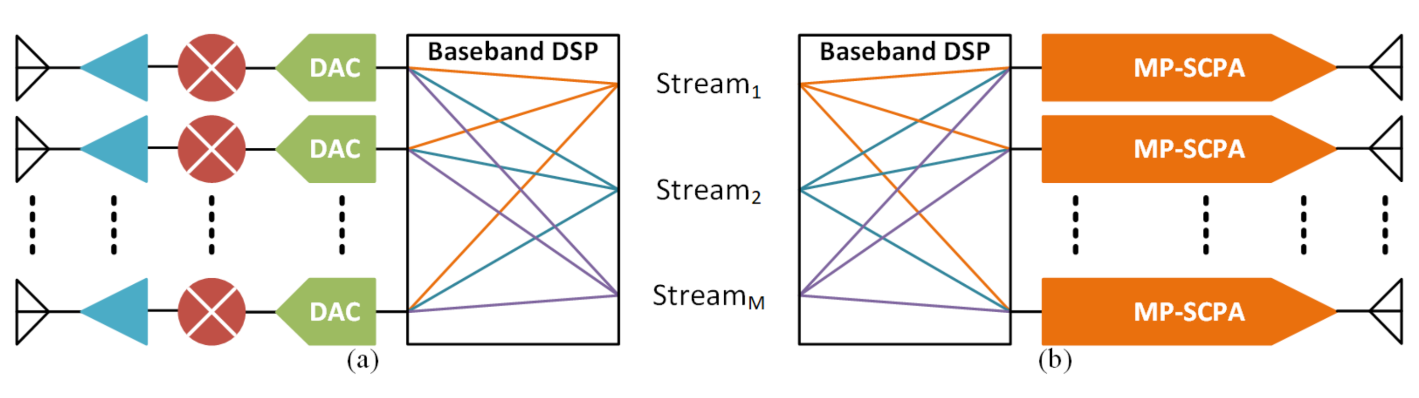
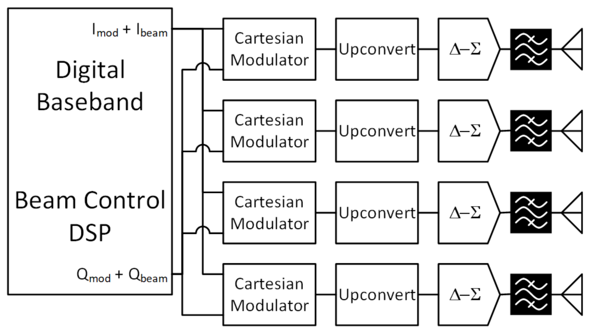
2. Review of Highly Digital Beamforming Transmitters/PAs

In traditional analog beamforming transmitters, the beam weighting is performed in either the IF/baseband, LO or RF paths, using either passive phase shifters (e.g., reflective [21]), or active phase shifters (e.g., Cartesian combiner [4], ring oscillators [2], etc.). In purely analog beamformers, only one beam can be formed per array. Digital beamforming makes it possible to operate with a single beam or with multiple beams using digital processing, but it can be costly in hardware and power consumption as it requires a DAC in every transmitter path.
Recently, DDRFs have been proposed for use in beamforming transmitters, as they combine the functions of data conversion, frequency translation and front-end amplification [22]. Such configurations naturally enable digital beamforming, as individual beams can be combined digitally in the baseband DSP and directly input to the DDRFs digital decoders, but to date, there have been limited reports of DDRFs being used in beamforming.
A pulse-based transmitter with digitally programmable pulse shape and delay elements was proposed by Wang, et al. for a UWB transmitter (Figure 2) [8]. In this transmitter, digitally programmable delay lines were used to linearly adjust the true time-delay between transmitter paths. Each of the paths is comprised of a cascade of digitally programmable delay elements. This implementation does not allow complex weighting between elements, as only the delay and pulse shape can be adjusted. Although using time delay, rather than phase shifting allows for a wider frequency bandwidth, the technique suffers from reduced phase resolution at higher frequency due to degradation in the performance of the delay elements.
A Cartesian phase shifter [4] was used in combination with a current-mode polar DPA by Qian, et al. to realize a DDRF beamforming transmitter (Figure 3) [9]. In this implementation, the phase shift required for beamforming is performed using a digitally weighted Cartesian phase shifter, before driving the RF input of a current-mode DPA. Amplitude weighting could be accomplished separately in the AM path, with the caveat that higher resolution would be needed to allow for both modulation and weighting. This implementation achieves outstanding phase accuracy at moderately high output power, owing to the polar DPA acting as an embedded transmitter, but the current-mode DPA requires digital pre-distortion (DPD) to correct for nonlinearity in the DPA. Operation in the polar domain affords high energy efficiency but suffers from challenges due to systematic nonlinearity.
A bandpass Δ Σ modulator (DSM) combined with an N-path filter [10] was proposed by Zheng, et al. (Figure 4). The inherently linear 1.5b Δ Σ DAC combined with the N-path filter reduces the transmitter area, while not requiring significant DSP. The architecture is promising, particularly for dense arrays in deeply scaled CMOS. Chip area reduction is critical for dense arrays, but it is notable that the DSM requires significant interpolation for oversampling, and the digital baseband consumes a fairly high amount of power, considering that the implementation does not include a high-power output stage. The implementation achieved excellent beam accuracy, but the bandwidth (<1 MHz) and error vector magnitude (EVM) were relatively limited (>3.5% at 400 MHz, >6.6% at 1.2 GHz; both for single-carrier 64-QAM) and it would probably require significantly increased power for more complex modulation.
To overcome the challenges of the aforementioned DDRF beamforming architectures, we propose multiphase interpolation beamforming using the SAMP-SCPA [12] (Figure 5). The SAMP-SCPA can output any required amplitude and phase at the rate that its decoders can operate. Multiphase signaling does not have the same inherent bandwidth limitations as polar signaling, and the SCPA is more linear than current-mode DPAs due to the use of ratioed capacitors. The addition of beamforming to the operation requires only modification to the logic decoder, which can perform the vector combination of modulation and beam weight. Finally, the SCPA allows for an embedded output-stage/power amplifier that can operate linearly at low power [23] and at powers exceeding 1 W [16,24]. Multiphase interpolation beamforming using an SAMP-SCPA is discussed in detail in the next sections.

3. Multiphase Interpolation Beamforming

The proposed beamforming transmitter block diagram schematic is shown in Figure 5. An SAMP-SCPA forms the core [14] of the multiphase interpolation beamforming transmitter. In the proposed transmitter, a multiphase (MP) clock is generated using a ring oscillator that is injection-locked to a global clock. Any conventional technique can generate the MP clock (e.g., multi-stage ring oscillator, MP DLL, polyphase RC filter, etc.) The MP is then passed to an MP logic decoder that selects the appropriate phase and encodes the appropriate amplitude of each phase in the digital domain, before the signal is reconstructed using the SAMP-SCPA as a power DAC.
The SCPA is a DPA where the original variants were all operated in the polar domain [7,25,26,27]. Digital polar operation requires a coordinate rotation digital computer (CORDIC) to convert a Cartesian signal (e.g., I + j Q ) into a polar signal (e.g., A e j ϕ ), which results in bandwidth expansion of both the amplitude (A) and phase ( ϕ ) components, due to the nonlinear conversion. Polar systems are problematic for wide bandwidth modulation due to the bandwidth truncation and timing misalignment that dominate the out-of-band noise and linearity [28]. Ideally, phase modulation is implemented with a phase-locked loop (PLL), but this is unsuitable for wider band modulation [29,30]. Quadrature modulation can be used to create wideband phase modulation [31], but if performed before the output stage it still requires precise time alignment with the amplitude signal, and if performed in the output stage it is subject to peak output power reduction [15,24,32].
The multiphase interpolator was proposed to overcome these challenges [13]. In multiphase modulation, the complex plane is subdivided into M-basis phases that can be weighted and summed to achieve an output at any arbitrary amplitude and phase. It should be noted that the multiphase modulator has recently shown superior linearity as a stand-alone phase modulator [33,34].

3.1. Single Multiphase Transmitter Operation

An example of multiphase vector addition is shown in Figure 6, where the complex plane is divided by M = 8 basis phases ( ϕ 0 ϕ 7 , Figure 6a). In the example, the approach to generating the vector v with amplitude A and phase θ is depicted. First the two adjacent basis phases of the clock, ϕ 0 and ϕ 1 , are selected (See Figure 6b), then they are individually weighted by basis phase weights n 1 and n 2 . The basis phase weights can first be found by mapping to the traditional Cartesian basis vectors, according to the following [13]:
n 1 = I · s i n ( 2 π ( m + 1 ) M ) Q · c o s ( 2 π ( m + 1 ) M ) s i n ( 2 π M ) , and
n 2 = I · s i n ( 2 π ( m ) M ) + Q · c o s ( 2 π ( m ) M ) s i n ( 2 π M ) .
A representative multiphase SCPA (MP-SCPA) is shown in Figure 6c. The weights n 1 and n 2 control how many of the capacitors are switched on ϕ 0 or ϕ 1 , respectively, and the sum of n 1 and n 2 is bound by the following:
0 < n 1 + n 2 < 2 k ,
where k represents the total number of bits in the array (e.g., 2 k = N ). Furthermore, n 1 and n 2 can be found in terms of A and θ using the following substitution for I and Q:
I = A · c o s ( θ ) , and
Q = A · s i n ( θ ) .
Substitution of (4) and (5) into (1) and (2) yields the following:
n 1 = A · c o s ( π M ) · s i n ( 2 π ( m 1 ) M θ ) s i n ( 2 π M ) , and
n 2 = A · c o s ( π M ) · s i n ( θ 2 π ( m 1 ) M ) s i n ( 2 π M ) .
It can be shown that the voltage amplitude V o u t of the output voltage across R o p t , for a given supply voltage, V D D and set of codes and basis phases is given by the following [13]:
V o u t = 2 · V D D π · n 1 2 + n 2 2 + 2 n 1 · n 2 · c o s ( 2 π M ) N .
The output power P o u t is given by the following:
P o u t = 2 π 2 · n 1 2 + n 2 2 + 2 n 1 · n 2 · c o s ( 2 π M ) N 2 · V D D 2 R o p t .
The input power P i n is the power required to switch the total input capacitance C i n :
P i n = C i n · V D D 2 · f 0 ,
where f 0 is the output frequency. C i n is given by the following:
C i n = ( n 1 ) · ( N n 1 ) N 2 + ( n 2 ) · ( N n 2 ) N 2 + 2 · n 1 · n 2 N 2 · C ,
where C is the value of a unit capacitor in the array. The total array capacitance can be selected to optimize matching (e.g., larger unit capacitors [35]) or efficiency at backoff, by controlling the network quality factor Q N W [13]. Split-array techniques allow a trade-off between the two [14].
The SCPA is a series resonant circuit where Q N W is given by the following:
Q N W = 1 2 · π · N · C · R o p t .
L s e r (Figure 6c) is chosen to be resonant with the total array capacitance:
L s e r = 1 N · C · ( 2 · π · f 0 ) 2 .
It is noted that the series resonant inductor and output resistor can be replaced with any load and an impedance matching network, where the aim of the matching transformation is to present a net inductive reactance and real impedance designed for the desired power level, according to (9).
With a known output power and input power, the drain efficiency η can be found according to the following:
η = 1 + P i n P o u t 1 .
Substituting (9)–(12) into (14) yields the following:
η = 1 + π · [ n 1 · ( N n 1 ) + n 2 · ( N n 2 ) ] 4 · Q N W · n 1 2 + n 2 2 + 2 · n 1 · n 2 · c o s 2 · π M 1 .
The efficiency can be found at any output power level and phase angle by appropriately selecting n 1 and n 2 according to (1) and (2). It is noted that choosing a larger Q N W increases the efficiency level at output power backoff, at the expense of output bandwidth.
Operation using split arrays such as the SAMP-SCPA do not change the operation as presented above, but they do allow the resolution of the SCPA to be arbitrarily controlled while also controlling Q N W . Additionally, it is noted that the multiphase technique originally proposed in [13] has been adapted for use only as a constant envelope phase modulator [33,34].

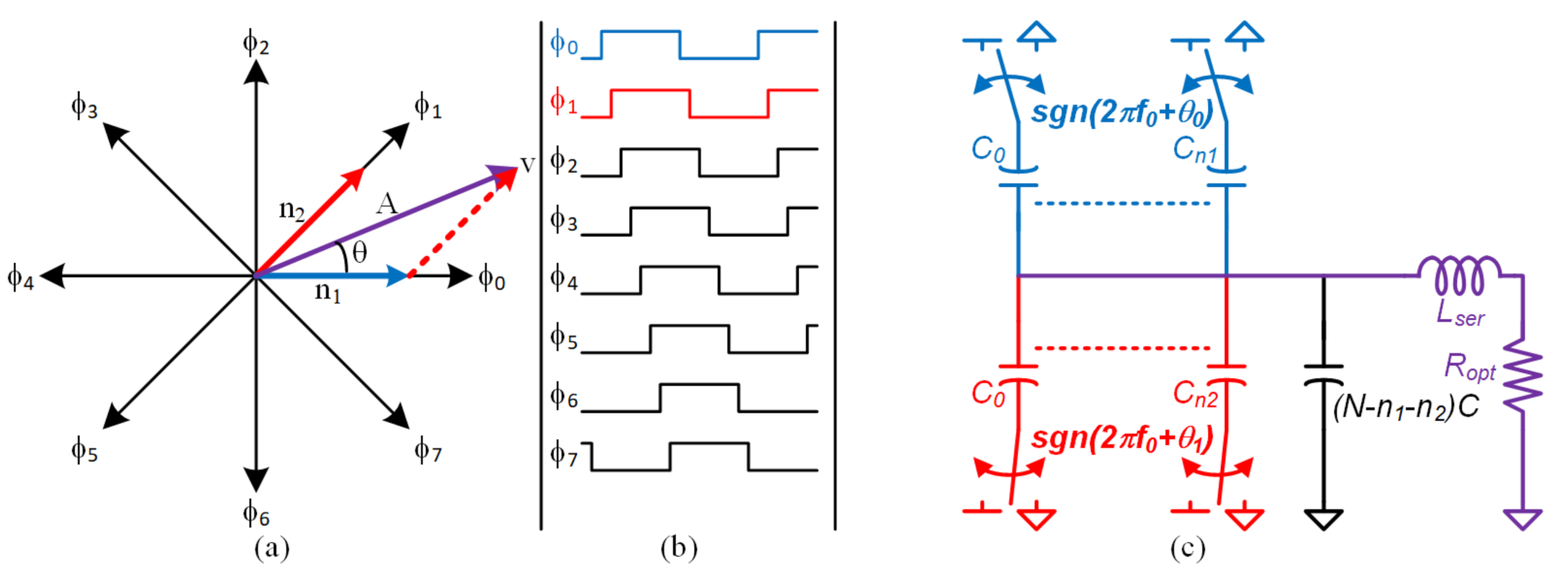
3.2. Amplitude and Phase Resolution in MP-SCPA

Both n 1 and n 2 are quantized values that are used to reconstruct arbitrary output amplitude and phase combinations. Because the number of available states decreases as the amplitude decreases, the phase resolution for small amplitudes also decreases. This is true for any digital multiphase transmitter, including the special cases of the quadrature digital transmitters (e.g., M = 4 ) [15,32]. Because the entire array can be switched fully by either ϕ 0 or ϕ 1 , or by a combination of the both, there are 2 k + 1 possible states between the basis phases. To illustrate, constant amplitude arcs are plotted for several values of M and k in Figure 7. It is noted visually that increasing the MP-SCPA resolution k increases both the amplitude and phase resolution, as would be expected. Similarly, increasing the number of phases increases both the amplitude and phase resolution, particularly for low output amplitudes, as the density of states in each cone between two adjacent phases increases as the number of basis phases M increases.
To quantify the impact of both k and M, simulations of an ideal MP-SCPA were run across the full output amplitude and phase range. The RMS phase error is plotted as a function of the normalized output amplitude for a k = 9 b array, for an ideal MP-SCPA with M = { 4 , 8 , 16 } , in Figure 8a. We note that as the number of phases is increased, the discrete number of amplitude/phase states covers a reduced amount of area, meaning that the RMS error would be expected to be reduced. As expected, when doubling the number of phases, the same RMS phase error can be achieved for 3 dB less power. The RMS amplitude error is plotted as a function of the normalized output amplitude for a k = 9 b array, for an ideal MP-SCPA with M = { 4 , 8 , 16 } , in Figure 8b. Increasing the number of phases does not have a significant impact on the RMS amplitude error at large amplitudes, but the increased density of states does have some impact at lower amplitude.
In MP-SCPAs, it was noted that as M is increased, the average power drop relative to a polar system is reduced at the expense of reduced time available for charge settling and hence reduced linearity [13]. It was noted that M = 16 resulted in a good trade-off between the power drop, efficiency and linearity. The RMS phase error is plotted versus normalized output amplitude for M = 16 and several different array resolutions in Figure 9a. For an array resolution of 10b, <1 RMS phase error can be achieved for ∼20 dB of output power range. The RMS amplitude error is plotted versus normalized output amplitude for M = 16 and several different array resolutions in Figure 9b. As expected, increasing the array resolution reduces the RMS amplitude error by ∼6 dB per bit of resolution.

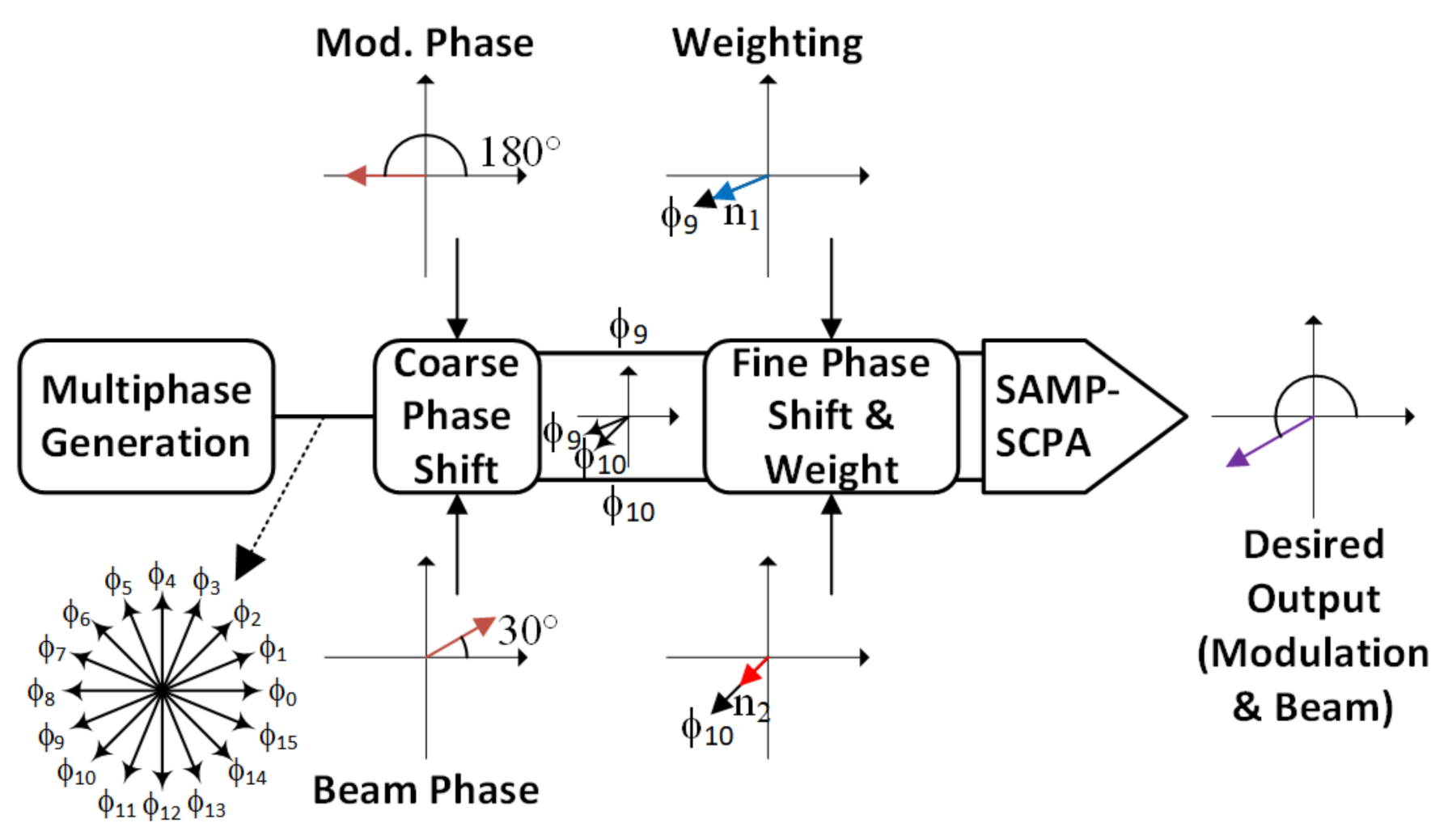
3.3. Multiphase Beamforming Operation Example

The operation of an MP-SCPA used in MP interpolation beamforming is explained by the block diagram schematic in Figure 10. First, a set of basis phases (e.g., ϕ 0 ϕ 15 ) that span the unit circle is generated by a multiphase clock generator. Next, the desired instantaneous modulation phase ( 180 ) and beam phase ( 30 ) are added as inputs into a phase selection logic that determines the total desired phase shift ( 210 ) and selects two adjacent phases ( ϕ A = 202 . 5 and ϕ B = 225 ) from the set of basis phases to this desired output phase. The desired amplitude of the output is next provided as an input, as the product of the instantaneous modulation envelope and the desired beam weighting. From this, the decoder determines n 1 and n 2 , the required weightings for ϕ A and ϕ B , respectively. Finally, these weights are applied to an SAMP-SCPA to determine how many of the cells are switched on ϕ A , how many are switched on ϕ B and how many are held at ground. In this way, the weighted basis phases are added on the SAMP-SCPA capacitor array to form a vector summation that contains the desired output amplitude and phase modulation, as well as the desired beam steering and weighting.
Unlike [9], which only applies digital phase shifting using a quadrature digital phase shifter at the input of a polar DPA, the proposed design allows for the amplitude and phase weighting to occur at the SAMP-SCPA, and the weighting can be completely controlled by an individual multiphase logic decoder, which saves power and area and allows direct recombination at the output stage.
In choosing the designed resolution, it is noted that the phase and amplitude control for the beam steering are simply added as offsets using a digital encoder. The resolution required for wideband wireless communication to suppress out-of-band noise and achieve in-band high fidelity (e.g., low EVM and ACLR) is higher than that required to achieve high phase and amplitude resolution for beam steering [14]. Hence, array resolution is primarily dictated by the in-band and out-of-band signal requirements of the communication signal to be transmitted.

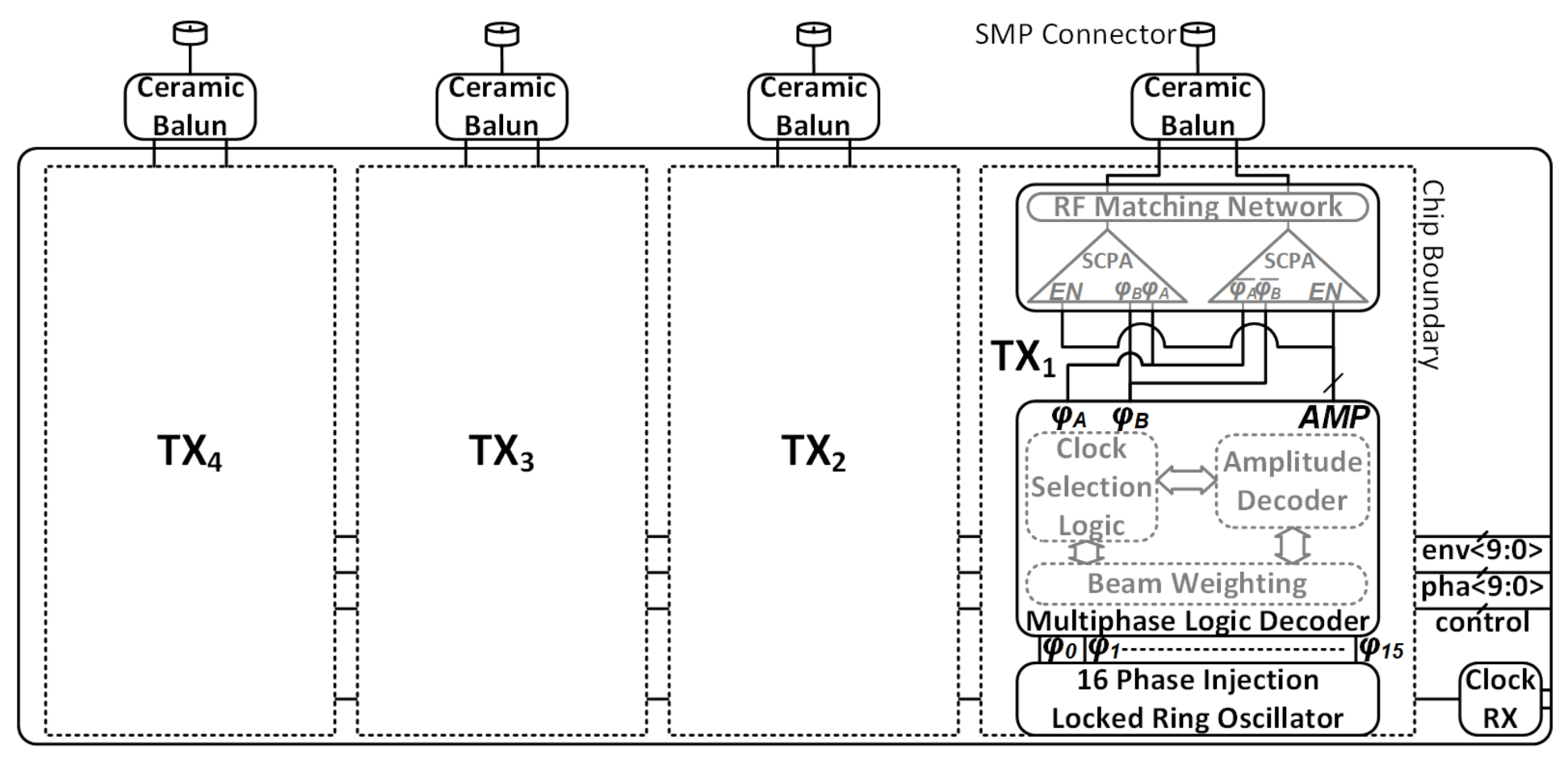
4. Circuit Design Details

The proposed four-element TX beamformer architecture is shown in Figure 5. It consists of four identical 16b TXs that each drive an off-chip ceramic balun and SMP connector jack for interfacing to an antenna. The resolution of the TX was chosen to be similar to the split-array MP-SCPA (SAMP-SCPA) previously presented in [14]. Whereas in that design the I/O was serialized, allowing the full array resolution to be tested, in this design the I/O remains parallelized. Hence, although the circuit is designed with a 16b array resolution, the measurement setup is limited to 22 I/O channels, meaning that only the upper 9b of the array could be utilized in the measurement setup. The circuit design details of all major blocks in the beamforming TX are now discussed.

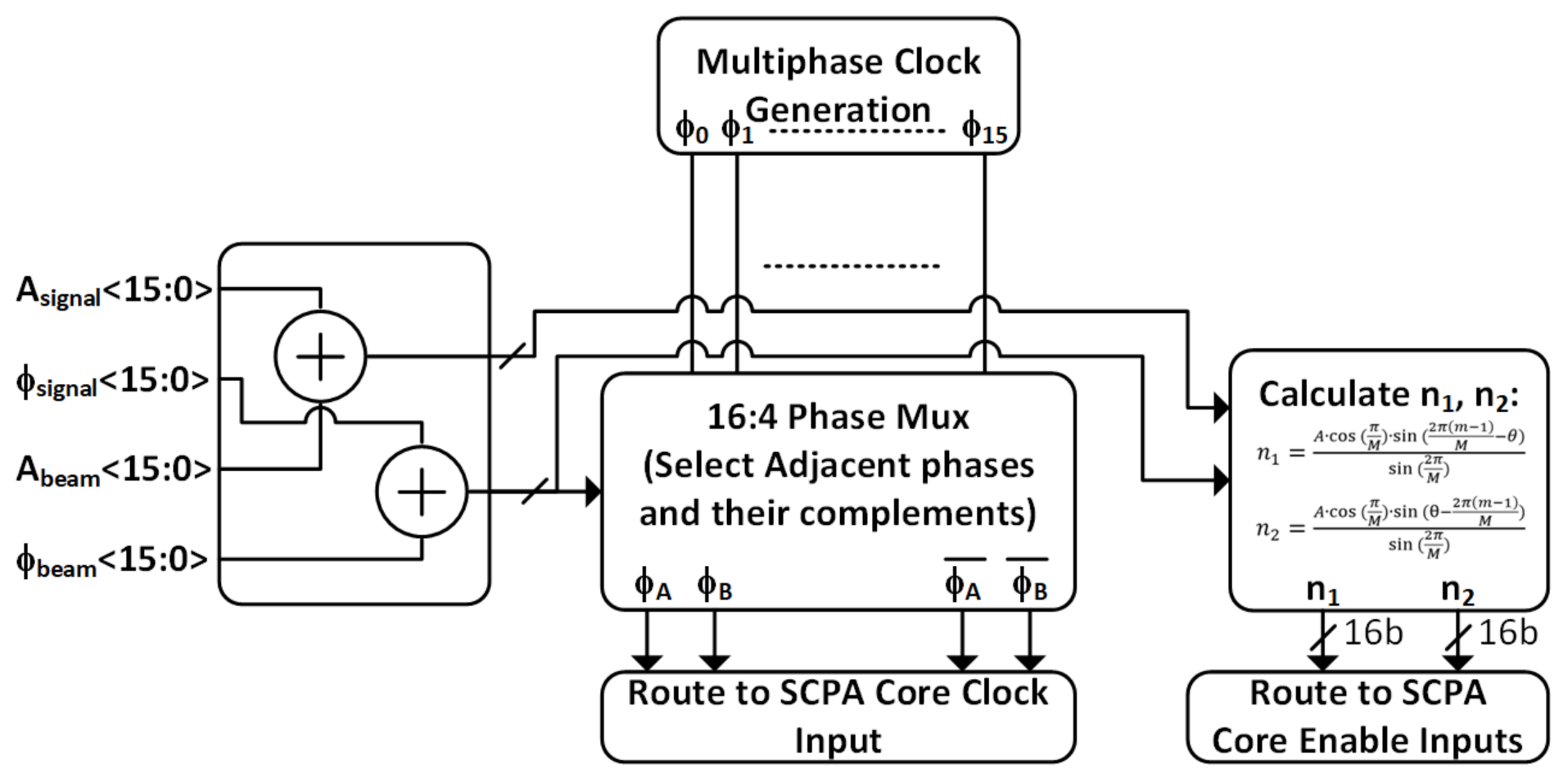
4.1. MP Clock Generation

Each TX has a local eight-stage pseudo-differential ring oscillator, as shown in Figure 11, which is injection-locked to a global clock to create 16 evenly spaced basis phases. The delay cell used in the ring oscillator is the Maneatis delay cell [36]. The global clock is input to the chip via an LVDS clock RX and care is taken to route the clock with an equal delay to each ring oscillator, to provide a common time/phase basis. In cases where layout/routing mismatches create too much phase variation, calibration can be implemented through control of the digital input codes of the individual TX slice. All phases are input into a MUX tree that is controlled by the MP logic decoder.

4.2. MP Logic Decoder
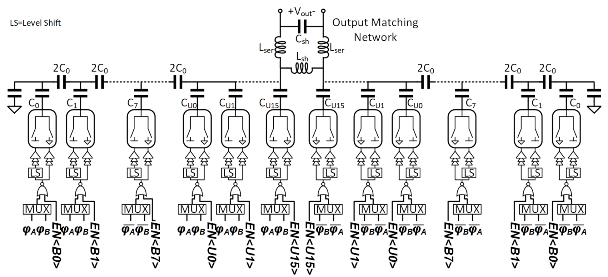
The MP logic decoder shown in Figure 12 takes as its input all basis phases from the MP clock generator and digital input codes representing the desired output phase and amplitude. An additional control bit allows each transmitter to separate beam weighting and modulation.
When the control bit is enabled, beam weighting and steering are performed in two steps. First, the clock selection logic chooses the two adjacent phases to the desired output phases. The clock selection logic uses 4 input bits and is used to select two adjacent phases ( ϕ A and ϕ B ) from the original input phases that will be routed to the SAMP-SCPA. At this stage, a course phase shift has been achieved, given that the output phase must be between the two input phases selected. Next, using a 16b amplitude and 16b phase code the decoder finds the weights, n 1 and n 2 for ϕ A and ϕ B , respectively, according to (1)–(7). In this way a fine beam weight and phase shift is achieved.
When the control bit is disabled, the prior weight and phase shift are stored as the desired spatial weighting for the beam to be formed. The amplitude and phase input can now be added to the stored beam weighting, resulting in the computation of new values for n 1 and n 2 and selection of new phases for a vector output, where the output amplitude is a product of the modulation envelope with the desired beam weight and the output phase is the sum of the beam phase and modulation phase, as discussed in Section 3.3.
The decoders that set the weights for n 1 and n 2 are identical cascaded binary-to-thermometer decoders [13]. The first 16b binary-to-thermometer decoder selects how many cells are switched by phase ϕ A . The second 16b binary-to-thermometer decoder selects whether the balance of the cells are switched by ϕ B or held at ground. All decoders are written in Verilog and then synthesized and automatically placed and routed.

4.3. 16-b SAMP-SCPA

The schematic for one of the SAMP-SCPA cores is shown in Figure 13. The SAMP-SCPA was chosen due to its ability to achieve good linearity and output power with high efficiency in a compact area [14]. The schematic and layout were performed in slices, where the entire cell was designed from input logic through to capacitor as an individual slice. Unary weighted cells were designed to be identical and C-2C cells were optimized so that their delay matched the unary cells, given that each C-2C cell drives a slightly different impedance. The individual layout slices were then tiled to realize the layout of the completed SCPA. The design of each element in the slice, shown in Figure 14, is now described starting from the input logic.

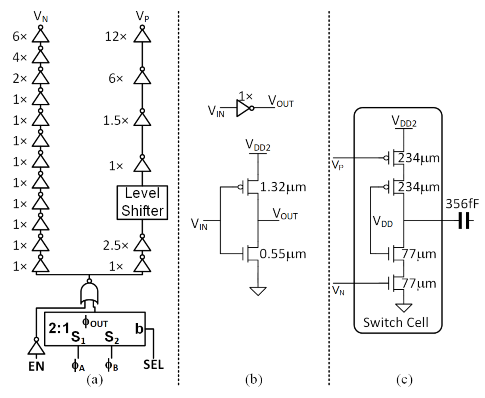
4.3.1. SAMP-SCPA Input Logic Design

The input to each cell of the SAMP-SCPA consists of two clock signals with identical frequency and a phase separation equal to 360 /M, a phase selection control (SEL) that determines whether to switch on the leading or lagging phase and an enable bit (EN) that enables/disables switching on the selected phase.
The clock signals are input into a static MUX, whose output is controlled by SEL. Any MUX implementation is appropriate, but a static NAND-NAND MUX was used for easy pitch matching with other cells in the layout. The output of the MUX drives one input of a static NOR gate whose other input is EN. When EN is low, the clock signal propagates to the switch driver chain, and when it is high, the clock signal is blocked from the driver chain. This saves power as the driver chain in each cell does not consume power when the cell is off. This also effectively closes the output switch to ground, helping the SCPA to present a constant impedance to the load.

4.3.2. Switch Driver Slice Design

After the input logic, a driver chain consisting of two parallel inverter chains (Figure 14a) was used to drive the output switch. In one path, a level shifter like the one proposed in [37] is used to convert the input logic level from V G N D - V D D to V D D - V D D 2 ( V D D 2 = 2 × V D D ). This path is used to drive the PMOS transistor in the switch (Figure 14c). Inverters after the level shifters are placed in deep N-wells to allow operation from the shifted supply rails. The other path operates between V G N D and V D D to drive the NMOS transistor in the switch. Each path is comprised of a cascade of scaled buffer cells based upon the unit cell, as shown in Figure 14b.
The driver slice is located adjacent to the switch and takes its input from the MP logic decoder, where the decoders outputs have been pitch-matched to the appropriate input in the array. Co-location of the logic and driving chains allows the parasitic routing capacitance to be minimized and easier timing synchronization of the switching signals.

4.3.3. Output Switch and Capacitor

To provide for a larger optimum termination impedance, which allows for reduced loss in the output matching network, the switch is composed of a cascoded CMOS inverter (Figure 14c). This topology allows each transistor in the stack to maintain no more than V D D across any two terminals. This is a feature of the SCPA that is unique amongst CMOS PAs. The switch widths are optimized to drive the slice capacitance optimizing the power/delay product.
In the unary MSB sub-array, all the unit capacitors in each path are identical, so the size for every switch in the unary MSB path is identical. In the C-2C LSB sub-array, the total equivalent input capacitance for each successive bit in a C-2C array increases linearly as the number of C-2C bits are increased. In addition, the nodal parasitic capacitance cannot be ignored when considering the total equivalent capacitance. Hence, the size of the transistor in the switch and the drivers in the C-2C LSB paths should be optimized, so that the delay is matched to that of the unary paths.
The capacitors are arrayed so that the output of the switch pairs with the top plate of the capacitor, which minimizes exposure of this node to the substrate. The bottom plates of every capacitor slice in the array are shared. The array is sub-divided into a 12b C-2C LSB sub-array and 4b unary MSB sub-array. The choice of array resolution was primarily dictated by the signal fidelity requirements and complexity/area in the layout, noting that for every additional unary bit, the number of cells doubles, whereas an additional binary bit only increases the cell count by one. In our case, it has been shown that signal fidelity requirements can be largely met using 9b-10b of array resolution. The choice of where to sub-divide the array also depends on the desired linearity and complexity of the thermometer decoder required for the unary weighted bits [14].
For the presented design, all these options were considered for the array size and segmentation before settling on the chosen values. Using a 4b unary and a 12b binary allows for a design that can meet the signal fidelity requirements and also makes digital pre-distortion possible if needed, due to excess “throw-away states”, all while not exceeding the assigned dimensions for each transmitter, which were dominated by I/O pad requirements and the size of the matching network, as discussed next.

4.3.4. Matching Network

The total capacitance in the array seen from the matching network remains constant, regardless of the input code. This is because when a switching cell is disabled, it holds the top plate of the capacitor at a constant potential through a fixed-value resistance such that the impedance seen looking into each slice of the array is constant. Hence, the matching network is unchanged for any choice of input code. The matching network shown in Figure 13 comprises a shunt inductor L s h , a series inductor L s e r and a shunt capacitor C s h , forming a band-pass network that presents R o p t to the capacitor array and is series resonant with the total array capacitance.
Each PA is matched to 50 Ω differentially at the pads on the chip. The bondwire inductance is in series with the PA output and is resonated with an off-chip capacitor at the center frequency of the band. An off-chip ceramic transformer balun is used to convert the output from differential to single-ended before connection to an SMP jack.
The on-chip matching and off-chip network serve to filter high-frequency harmonics that arise due to the switching behavior. The −3 dB output power bandwidth is ∼700 MHz, centered at 1.8 GHz. The bandwidth is determined by the Q N W ( 3 ) of the band-pass matching network. Q N W is primarily chosen to maximize the efficiency of the topology while minimizing loss in the impedance transformation network. If off-chip impedance transformations are used, a higher Q N W can be chosen.

5. Experimental Results

A prototype four-element beamforming TX was fabricated in a 65 nm RF CMOS process with nine metal layers, including an ultra-thick top metal for high-quality passive components. The chip microphotograph is shown in Figure 15a. The combined area of all four TXs is 5 mm 2 , including the matching network, output stage, logic decoders and the I/O pad frame. The chip area is dominated by the I/O pad requirements and could be reduced in an SOC implementation. All circuits operate at 1.4 V, except for the cascaded switches that operate at 2.8 V. The TX array is chip-on-board bonded to a PCB, and an off-chip transformer balun converts the differential signal to single-ended to drive an SMP jack, as shown in Figure 15b. An external clock signal is received by an on-chip low-voltage differential signaling (LVDS) amplifier and is used to injection-lock the multistage ring oscillators in every path. The digital I/O is input from a high-speed digital I/O (HSDIO) pattern generator and is composed of the bits to control phase selection and the fine phase and amplitude control of each SAMP-SCPA. The HSDIO that was used limited the number of available I/O lines to 24, meaning that only the 9b of the array for each SAMP-SCPA could be utilized. MSBs were favored due to their larger impact on output power and efficiency. Individual TXs were characterized for both their static and dynamic (modulated) characteristics and beamforming measurements as follows.

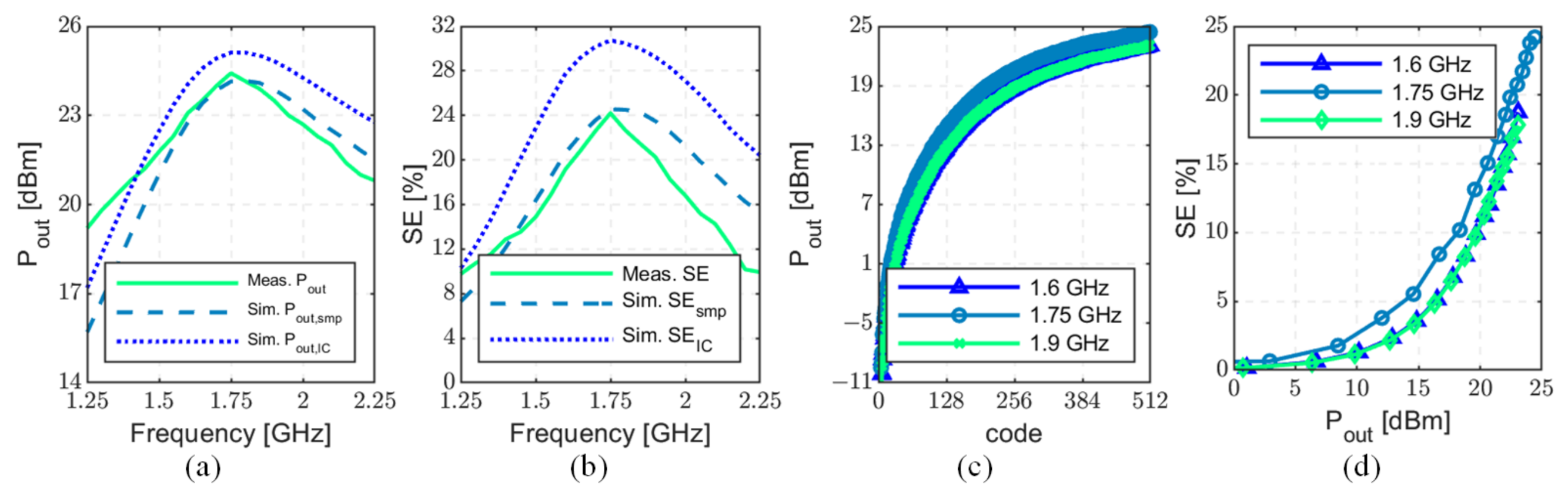
5.1. Static Measurements

The individual TXs showed similar measured performance. The measurements considered all losses including those of the off-chip balun and SMP connector. The measured peak output power P o u t and the system efficiency (SE) versus the frequency are plotted in Figure 16a,b, respectively. A peak output power and SE of 24.4 dBm and 24.2% were observed at the center frequency of 1.75 GHz, respectively. Also plotted are the simulated output power at the connector P o u t , s m p and the simulated output power at the IC periphery P o u t , I C , shown in Figure 16a. In Figure 16b, the simulated SE is plotted at the connector, S E s m p and the IC periphery S E I C . The measured output power versus input code and measured SE versus output power at three frequencies across the band are shown in Figure 16c,d, respectively. It is again noted that SE is measured at the connector, rather than wafer probed, which is what accounts for the reduced peak efficiency compared to other recently reported DPAs. The sharp roll-off in performance away from the center frequency is due to an external capacitor that is used to resonate the bondwire inductance from the packaging and due also to a ceramic transformer balun that is placed at the output of each PA.

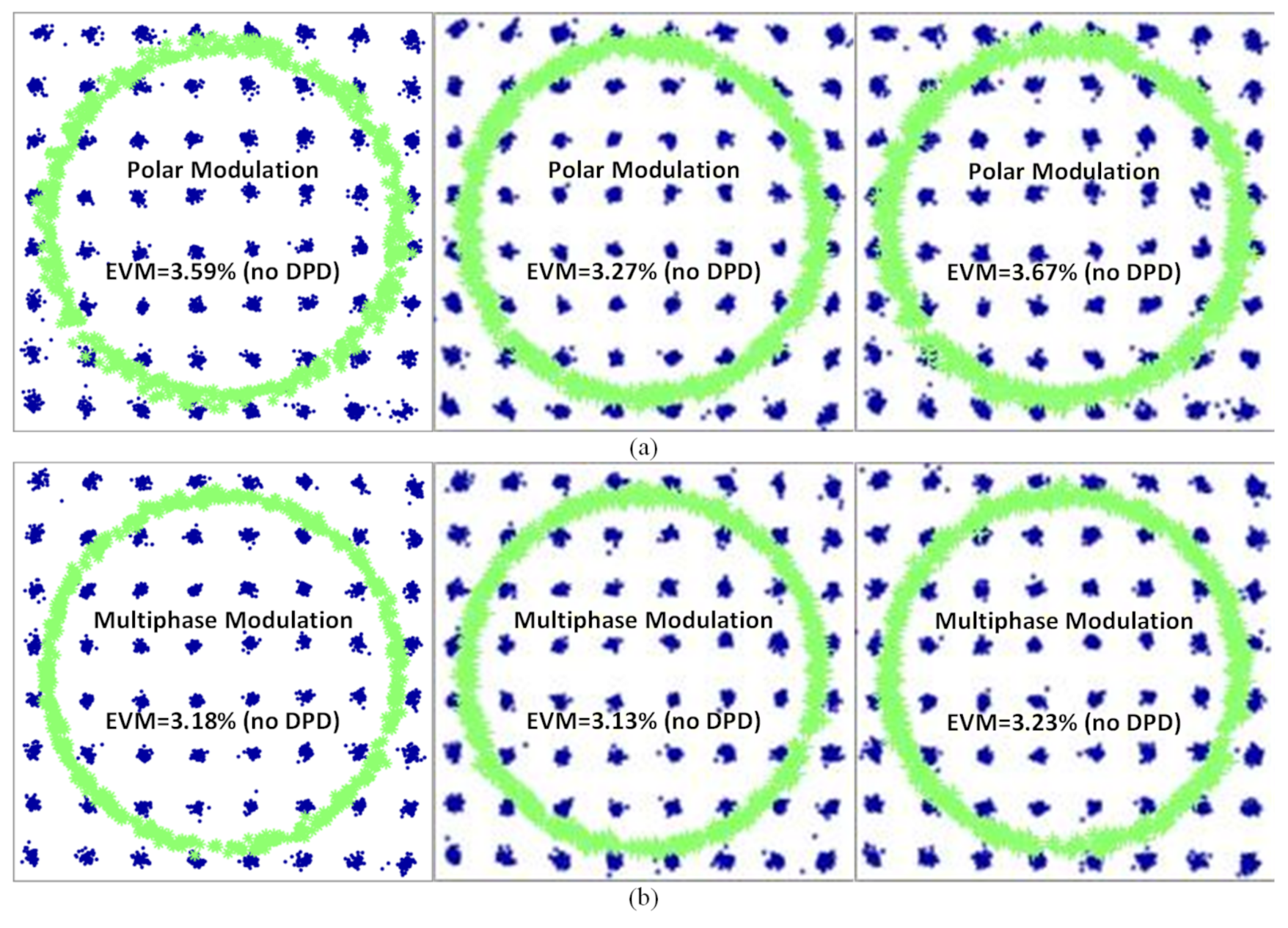
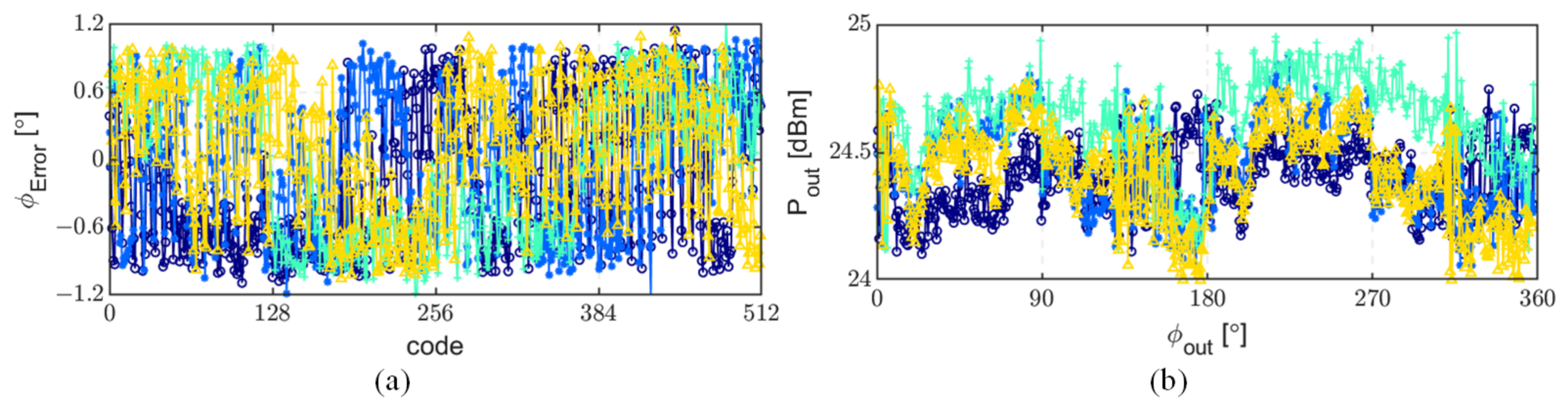
5.2. Dynamic Measurements

To verify the individual TX performance with signals with large PAPR, it was tested in both a polar mode, where the injected clock is phase modulated, and in a full multiphase mode, where the injected clock has a static input phase. In the polar modulation mode, a 15 MHz, 64 QAM, OFDM modulated signal was input to the PA, and in the multiphase mode, a 10 MHz, 64 QAM, OFDM modulated signal was input to the PA. The bandwidth was limited by the fact that the data clock buffering was undersized, to drive the input parasitic at a higher desired data rate. This was due to legacy circuits that were used on the much larger four-element chip. The problem was discovered after fabrication, and it limited the data clock to a rate of 150 MHz.
The measured PSD is shown for both the polar case and the multiphase case at low, center and high frequency, in Figure 17. The measured ACLR was <−30 dBc for all measurements. The ACLR level is largely determined by de-troughing. The signal is de-troughed to reduce the PAPR until it just meets the −30 dBc ACLR limit for E-UTRA [38]. De-troughing could be reduced to improve the ACLR at the expense of reduced output power and efficiency. It is noted that, in the polar case, systematic nonlinearities due to bandwidth limitation and timing mismatch create large spectral aliases. The measured signal constellations are shown for the polar and multiphase modulation cases at low, center and high frequencies, in Figure 18. The measured EVM for the signal is found to be <4% RMS across all frequencies and output beam angles.
Due to the linearity of the transmitter, digital pre-distortion (DPD) is not used at any frequency and ACLR and EVM are maintained across the band. Prior work has shown that for the 64 QAM OFDM signal used, the primary degradation to linearity is due to supply network parasitics (e.g., packaging inductance and resistance and on-chip/off-chip decoupling capacitance) [39]. To mitigate supply-network-dependent nonlinearity, we adopted staggered “de-Q” decoupling capacitors to maintain a low supply network impedance across frequency, while reducing ringing due to high-Q resonances [31,40].
The wideband power spectral density for both polar and multiphase transmission is plotted in Figure 19a. The out-of-band noise is typical for a DPA with 9b of resolution. Additionally, the signal is measured as the phase angle is arbitrarily controlled between 0 and 360 . The EVM is plotted vs. output phase angle for an individual transmitter, as shown in Figure 19b.

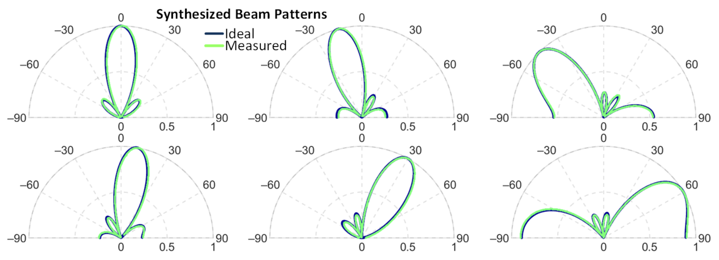
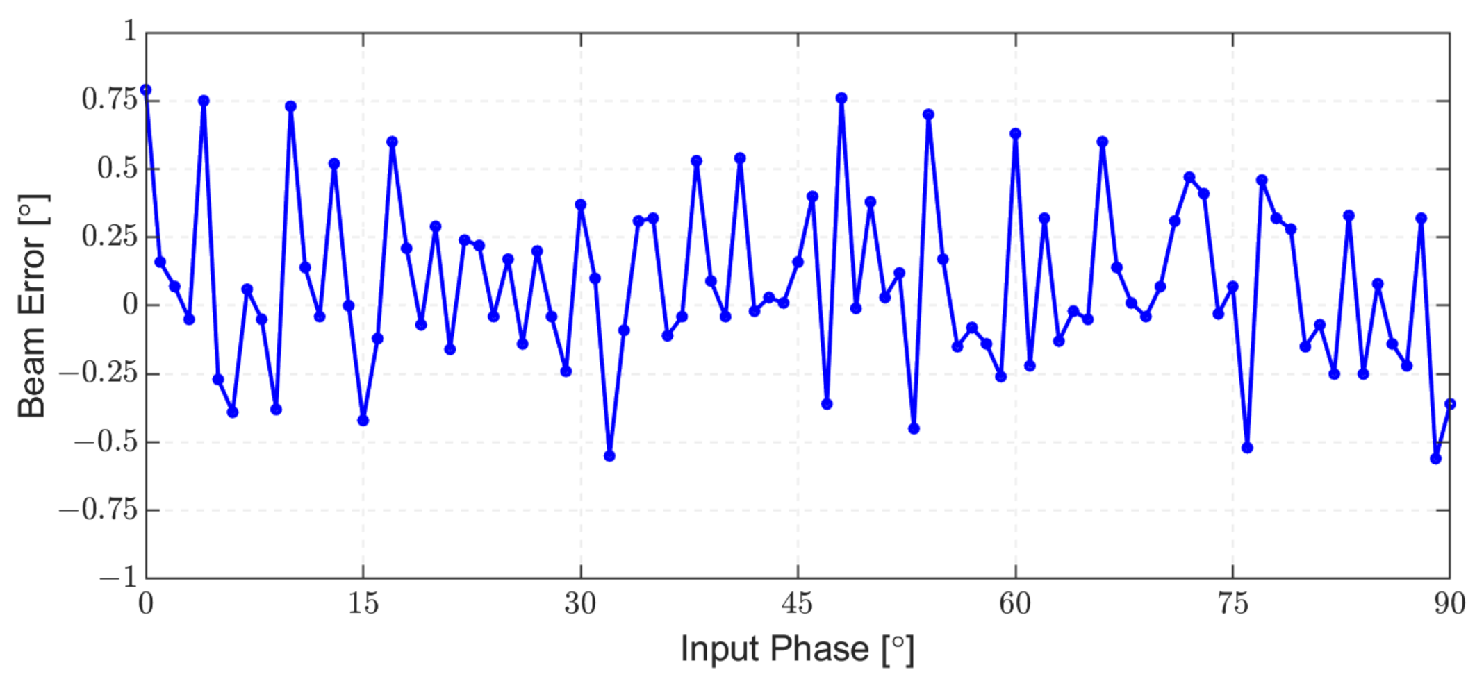
5.3. Beamforming Measurements

To validate the ability to form beams, four TXs on a single die were measured for their performance across the 9b phase control code range. The phase error is plotted as a function of phase code in Figure 20a. There was a static phase offset in the initial measurements that was corrected with a static off-line calibration. After the calibration, the phase error was < ± 1 across the 9b code range.
The output power is plotted as a function of output phase in Figure 20b for each of the four TXs and varies by <±0.5 dB for outputs across the code range. No amplitude calibration was applied.
To estimate the performance of the four independent elements in beamforming, the array factor was synthesized using the measured data for several pointing directions for a linear array with λ / 2 spacing. The measured transmitter data from four transmitters on a single die was fully characterized across the desired beam amplitude and phase. This measured data was then used to synthesize the array factor and hence the beam pattern, given the assumptions about antenna element spacing. The same pattern was synthesized for a linear array with ideal transmitters, and the two patterns are compared in Figure 21. The synthesized beam from the measured data matches well with the ideal synthesized beam across all output phases. The beam phase error as a function of ideal output phase angle is plotted for the synthesized pattern based on measured transmitters, in Figure 22. The resulting phase error across all patterns was 0 . 32 RMS.

6. Discussion

A four-element beamforming TX was introduced and implemented in 65 nm CMOS. The beamformer leverages multiphase interpolation to enable beam steering and beam weighting without the need for external phase shifters or individual DACs for each element. The technique can leverage any DPA to act as the weighting element, because DPAs are band-pass transmitters that simultaneously enable frequency translation and data conversion, and can operate with a large effective gain in a small die area. This is because in band-pass DPAs, the output reconstruction filter is a band-pass filter that is often smaller than the low-pass baseband filters that are used in conventional up-converting transmitters. The SCPA, which in recent years has been relabeled an SC-RFDAC or a C-DAC DPA, was chosen as the DPA to simultaneously realize high linearity and power and system efficiency with a small die area. When operating at 1.75 GHz, all four TXs can deliver a peak Pout of 24.4 dBm with 24.2% SE, while achieving <1 phase resolution and <1 dB gain error. The performance was validated by static and dynamic (modulation) measurements using both polar mode and multiphase mode without the use of DPD. The ACLR was below the required −30 dBc LTE standard for both modes, and the measured EVM was 3.27% RMS and 3.13% RMS, respectively.
A comparison with the prior state of the art for digital beamforming transmitters is provided in Table 1. Compared to [9], which is the most closely related work, the proposed work achieves similar phase and amplitude resolution but at higher output power and without the use of DPD, while achieving better linearity (ACLR and EVM). This is partially due to the use of the multiphase technique, which does not have the systematic nonlinearities of polar modulation, but is primarily due to the use of the SCPA, which is more linear than the current-mode DPA. Additionally, beam amplitude weighting is natively included in the proposed work. A comparison with the prior state of the art for recent DPAs and DTXs is provided in Table 2. The DPA performance alone compares well to other recent DPAs, and we note that it is the only one measured at the connector, rather than wafer probed. Because of the relatively high output power and small area, and the ability to independently weight the output beam and adapt its angle on an element-by-element basis in the digital domain, this can be deployed in large-scale antenna arrays used for both beamforming and for MIMO.

Author Contributions

Conceptualization, J.S.W., A.A., W.Y. and Z.B.; methodology, J.S.W., A.A. and Z.B.; validation, J.S.W., W.Y. and Z.B.; writing—original draft preparation, J.S.W. and Z.B.; writing—review and editing, J.S.W. and Z.B.; visualization, J.S.W. and Z.B.; supervision, J.S.W.; project administration, J.S.W.; funding acquisition, J.S.W. All authors have read and agreed to the published version of the manuscript.

Funding

This research was funded by the National Science Foundation under grant number #NSF-1508701.

Institutional Review Board Statement

Not applicable.

Informed Consent Statement

Not applicable.

Data Availability Statement

Not applicable.

Acknowledgments

The authors wish to acknowledge the support and assistance the National Science Foundation under grant #NSF-1508701. The authors also wish to acknowledge helpful discussions with Jeyanandh Paramesh and Sangmin Yoo.

Conflicts of Interest

The authors declare no conflict of interest.

References

  1. Hashemi, H.; Guan, X.; Komijani, A.; Hajimiri, A. A 24-GHz SiGe phased-array receiver-LO phase-shifting approach. IEEE Trans. Microw. Theory Tech. 2005, 53, 614–626. [Google Scholar] [CrossRef] [Green Version]
  2. Krishnaswamy, H.; Hashemi, H. A Variable-Phase Ring Oscillator and PLL Architecture for Integrated Phased Array Transceivers. IEEE J. Solid-State Circuits 2008, 43, 2446–2463. [Google Scholar] [CrossRef]
  3. Ta, T.T.; Tanifuji, S.; Kameda, S.; Suematsu, N.; Takagi, T.; Tsubouchi, K. A Si-CMOS 5-bit baseband phase shifter using fixed gain amplifier matrix. In Proceedings of the 2012 7th European Microwave Integrated Circuit Conference, Amsterdam, The Netherlands, 29–30 October 2012; pp. 576–579. [Google Scholar]
  4. Paramesh, J.; Bishop, R.; Soumyanath, K.; Allstot, D. A four-antenna receiver in 90-nm CMOS for beamforming and spatial diversity. IEEE J. Solid-State Circuits 2005, 40, 2515–2524. [Google Scholar] [CrossRef]
  5. Koh, K.J.; Rebeiz, G.M. An X- and Ku-Band 8-Element Phased-Array Receiver in 0.18-μm SiGe BiCMOS Technology. IEEE J. Solid-State Circuits 2008, 43, 1360–1371. [Google Scholar] [CrossRef]
  6. Paro Filho, P.E.; Ingels, M.; Wambacq, P.; Craninckx, J. An Incremental-Charge-Based Digital Transmitter with Built-in Filtering. IEEE J. Solid-State Circuits 2015, 50, 3065–3076. [Google Scholar] [CrossRef]
  7. Yoo, S.M.; Walling, J.S.; Woo, E.C.; Jann, B.; Allstot, D.J. A Switched-Capacitor RF Power Amplifier. IEEE J. Solid-State Circuits 2014, 46, 2977–2987. [Google Scholar] [CrossRef]
  8. Wang, L.; Lian, Y.; Heng, C.H. 3–5 GHz 4-Channel UWB Beamforming Transmitter with 1 Scanning Resolution Through Calibrated Vernier Delay Line in 0.13-μm CMOS. IEEE J. Solid-State Circuits 2012, 47, 3145–3159. [Google Scholar] [CrossRef]
  9. Qian, H.J.; Zhou, J.; Yang, B.; Luo, X. A 4-Element Digital Modulated Polar Phased-Array Transmitter With Phase Modulation Phase-Shifting. IEEE J. Solid-State Circuits 2021, 56, 3331–3347. [Google Scholar] [CrossRef]
  10. Zheng, B.; Jie, L.; Bell, J.; He, Y.; Flynn, M.P. A Two-Beam Eight-Element Direct Digital Beamforming RF Modulator in 40-nm CMOS. IEEE Trans. Microw. Theory Tech. 2019, 67, 2569–2579. [Google Scholar] [CrossRef]
  11. McCune, E.W. Concurrent polar and quadrature modulator. In Proceedings of the WAMICON 2014, Tampa, FL, USA, 6 June 2014; pp. 1–4. [Google Scholar] [CrossRef]
  12. Bai, Z.; Yuan, W.; Azam, A.; Walling, J.S. A Multiphase Interpolating Digital Power Amplifier for TX Beamforming in 65nm CMOS. In Proceedings of the 2019 IEEE International Solid- State Circuits Conference—(ISSCC) 2019, San Francisco, CA, USA, 17–21 February 2019; pp. 78–80. [Google Scholar] [CrossRef]
  13. Yuan, W.; Walling, J.S. A Multiphase Switched Capacitor Power Amplifier. IEEE J. Solid-State Circuits 2017, 52, 1320–1330. [Google Scholar] [CrossRef]
  14. Bai, Z.; Azam, A.; Johnson, D.; Yuan, W.; Walling, J.S. Split-Array, C-2C Switched-Capacitor Power Amplifiers. IEEE J. Solid-State Circuits 2018, 53, 1666–1677. [Google Scholar] [CrossRef]
  15. Alavi, M.S.; Staszewski, R.B.; de Vreede, L.C.N.; Long, J.R. A Wideband 2×13-bit All-Digital I/Q RF-DAC. IEEE Trans. Microw. Theory Tech. 2014, 62, 732–752. [Google Scholar] [CrossRef]
  16. Bhat, R.; Zhou, J.; Krishnaswamy, H. Wideband Mixed-Domain Multi-Tap Finite-Impulse Response Filtering of Out-of-Band Noise Floor in Watt-Class Digital Transmitters. IEEE J. Solid-State Circuits 2017, 52, 3405–3420. [Google Scholar] [CrossRef]
  17. Hashemi, M.; Shen, Y.; Mehrpoo, M.; Alavi, M.S.; de Vreede, L.C.N. An Intrinsically Linear Wideband Polar Digital Power Amplifier. IEEE J. Solid-State Circuits 2017, 52, 3312–3328. [Google Scholar] [CrossRef]
  18. Park, J.S.; Wang, Y.; Pellerano, S.; Hull, C.; Wang, H. A CMOS Wideband Current-Mode Digital Polar Power Amplifier with Built-In AM–PM Distortion Self-Compensation. IEEE J. Solid-State Circuits 2018, 53, 340–356. [Google Scholar] [CrossRef]
  19. Zhang, A.; Chen, M.S.W. A Watt-Level Phase-Interleaved Multi-Subharmonic Switching Digital Power Amplifier. IEEE J. Solid-State Circuits 2019, 54, 3452–3465. [Google Scholar] [CrossRef]
  20. Yin, Y.; Li, T.; Xiong, L.; Li, Y.; Min, H.; Yan, N.; Xu, H. A Broadband Switched-Transformer Digital Power Amplifier for Deep Back-Off Efficiency Enhancement. IEEE J. Solid-State Circuits 2020, 55, 2997–3008. [Google Scholar] [CrossRef]
  21. Zarei, H.; Allstot, D. A low-loss phase shifter in 180 nm CMOS for multiple-antenna receivers. In Proceedings of the 2004 IEEE International Solid-State Circuits Conference (IEEE Cat. No.04CH37519), San Francisco, CA, USA, 15–19 February 2004; Volume 1, pp. 392–534. [Google Scholar] [CrossRef]
  22. Walling, J.S. The Switched-Capacitor Power Amplifier: A Key Enabler for Future Communications Systems. In Proceedings of the IEEE 45th European Solid State Circuits Conference (ESSCIRC), Cracow, Poland, 23–26 September 2019; pp. 18–24. [Google Scholar] [CrossRef]
  23. Fulde, M.; Belitzer, A.; Boos, Z.; Bruennert, M.; Fritzin, J.; Geltinger, H.; Groinig, M.; Gruber, D.; Gruenberger, S.; Hartig, T.; et al. A digital multimode polar transmitter supporting 40MHz LTE Carrier Aggregation in 28nm CMOS. In Proceedings of the 2017 IEEE International Solid-State Circuits Conference (ISSCC), San Francisco, CA, USA, 5–9 February 2017; pp. 218–219. [Google Scholar] [CrossRef]
  24. Yoo, S.W.; Hung, S.C.; Yoo, S.M. A Watt-Level Quadrature Class-G Switched-Capacitor Power Amplifier With Linearization Techniques. IEEE J. Solid-State Circuits 2019, 54, 1274–1287. [Google Scholar] [CrossRef]
  25. Kavousian, A.; Su, D.K.; Hekmat, M.; Shirvani, A.; Wooley, B.A. A Digitally Modulated Polar CMOS Power Amplifier With a 20-MHz Channel Bandwidth. IEEE J. Solid-State Circuits 2008, 43, 2251–2258. [Google Scholar] [CrossRef]
  26. Presti, C.D.; Carrara, F.; Scuderi, A.; Asbeck, P.M.; Palmisano, G. A 25 dBm Digitally Modulated CMOS Power Amplifier for WCDMA/EDGE/OFDM With Adaptive Digital Predistortion and Efficient Power Control. IEEE J. Solid-State Circuits 2009, 44, 1883–1896. [Google Scholar] [CrossRef]
  27. Yoo, S.M.; Walling, J.S.; Degani, O.; Jann, B.; Sadhwani, R.; Rudell, J.C.; Allstot, D.J. A Class-G Switched-Capacitor RF Power Amplifier. IEEE J. Solid-State Circuits 2013, 48, 1212–1224. [Google Scholar] [CrossRef]
  28. Walling, J.S.; Allstot, D.J. Design considerations for supply modulated EER power amplifiers. In Proceedings of the WAMICON 2013, Orlando, FL, USA, 7–9 April 2013; pp. 1–4. [Google Scholar] [CrossRef]
  29. Staszewski, R.; Muhammad, K.; Leipold, D.; Hung, C.M.; Ho, Y.C.; Wallberg, J.; Fernando, C.; Maggio, K.; Staszewski, R.; Jung, T.; et al. All-digital TX frequency synthesizer and discrete-time receiver for Bluetooth radio in 130-nm CMOS. IEEE J. Solid-State Circuits 2004, 39, 2278–2291. [Google Scholar] [CrossRef]
  30. Boos, Z.; Menkhoff, A.; Kuttner, F.; Schimper, M.; Moreira, J.; Geltinger, H.; Gossmann, T.; Pfann, P.; Belitzer, A.; Bauernfeind, T. A fully digital multimode polar transmitter employing 17b RF DAC in 3G mode. In Proceedings of the 2011 IEEE International Solid-State Circuits Conference, San Francisco, CA, USA, 20–24 February 2011; pp. 376–378. [Google Scholar] [CrossRef]
  31. Ye, L.; Chen, J.; Kong, L.; Alon, E.; Niknejad, A.M. Design Considerations for a Direct Digitally Modulated WLAN Transmitter With Integrated Phase Path and Dynamic Impedance Modulation. IEEE J. Solid-State Circuits 2013, 48, 3160–3177. [Google Scholar] [CrossRef]
  32. Jin, H.; Kim, D.; Kim, B. Efficient Digital Quadrature Transmitter Based on IQ Cell Sharing. IEEE J. Solid-State Circuits 2017, 52, 1345–1357. [Google Scholar] [CrossRef]
  33. Li, T.; Xiong, L.; Yin, Y.; Liu, Y.; Min, H.; Yan, N.; Xu, H. A Wideband Digital Polar Transmitter with Integrated Capacitor-DAC-Based Constant-Envelope Digital-to-Phase Converter. In Proceedings of the 2019 IEEE Radio Frequency Integrated Circuits Symposium (RFIC), Boston, MA, USA, 2–4 June 2019; pp. 83–86. [Google Scholar] [CrossRef]
  34. Madoglio, P.; Palaskas, Y.; Angel, J.; Tomasik, J.; Hampel, S.; Schubert, P.; Preyler, P.; Mayer, T.; Bauernfeind, T.; Plechinger, P.; et al. A Cellular Multiband DTC-Based Digital Polar Transmitter With -153-dBc/Hz Noise in 14-nm FinFET. IEEE J. Solid-State Circuits 2020, 55, 1830–1841. [Google Scholar] [CrossRef]
  35. Xiong, W.; Guo, Y.; Zschieschang, U.; Klauk, H.; Murmann, B. A 3-V, 6-Bit C-2C Digital-to-Analog Converter Using Complementary Organic Thin-Film Transistors on Glass. IEEE J. Solid-State Circuits 2010, 45, 1380–1388. [Google Scholar] [CrossRef]
  36. Maneatis, J.; Horowitz, M. Precise delay generation using coupled oscillators. IEEE J. Solid-State Circuits 1993, 28, 1273–1282. [Google Scholar] [CrossRef] [Green Version]
  37. Serneels, B.; Piessens, T.; Steyaert, M.; Dehaene, W. A high-voltage output driver in a 2.5-V 0.25-/spl mu/m CMOS technology. IEEE J. Solid-State Circuits 2005, 40, 576–583. [Google Scholar] [CrossRef]
  38. Jeong, J.; Kimball, D.F.; Kwak, M.; Hsia, C.; Draxler, P.; Asbeck, P.M. Modeling and Design of RF Amplifiers for Envelope Tracking WCDMA Base-Station Applications. IEEE Trans. Microw. Theory Tech. 2009, 57, 2148–2159. [Google Scholar] [CrossRef]
  39. Bai, Z.D.; Yuan, W.; Azam, A.; Walling, J.S. Multiphase Switched-Capacitor Power Amplifiers and Bandpass Digital Transmitters. IEEE RFIC Virtual J. 2016, 8, 1–12. [Google Scholar] [CrossRef]
  40. Chowdhury, D.; Hull, C.D.; Degani, O.B.; Wang, Y.; Niknejad, A.M. A Fully Integrated Dual-Mode Highly Linear 2.4 GHz CMOS Power Amplifier for 4G WiMax Applications. IEEE J. Solid-State Circuits 2009, 44, 3393–3402. [Google Scholar] [CrossRef]
Figure 1. Digital beamformer using: (a) traditional up-converting transmitter; (b) beamweighting direct-digital bits-to-RF transmitter.
Chips 01 00004 g001
Figure 2. DDRF used in UWB digital beamformer [8].
Chips 01 00004 g002
Figure 3. DDRF used in a polar digital beamformer [9].
Chips 01 00004 g003
Figure 4. DDRF used in a quadrature Δ Σ beamformer [10].
Chips 01 00004 g004
Figure 5. Block diagram schematic of a 4-element multiphase TX beamformer using a split-array multiphase SCPA.
Chips 01 00004 g005
Figure 6. (a) Example of multiphase vector addition for 8 basis phase vectors in the complex plane. (b) The associated time-domain waveforms of the basis-phase vectors. (c) Simplified schematic of a multiphase SCPA.
Chips 01 00004 g006
Figure 7. Constant amplitude contours normalized to A = { 1 , 1 / 2 , 1 / 8 } for: (a) M = 4 , k = 3 ; (b) M = 8 , k = 3 ; (c) M = 4 , k = 6 ; (d) M = 8 , k = 6 .
Chips 01 00004 g007
Figure 8. (a) RMS phase error vs. normalized output amplitude for an ideal 9b MP-SCPA for varying numbers of phases M and (b) RMS amplitude error vs normalized output amplitude for an ideal 9b MP-SCPA for varying numbers of phases M.
Chips 01 00004 g008
Figure 9. (a) RMS phase error vs. normalized output amplitude for an ideal 9b MP-SCPA for various resolutions k and (b) RMS amplitude error vs. normalized output amplitude for an ideal 9b MP-SCPA for various resolutions k.
Chips 01 00004 g009
Figure 10. Block diagram schematic of MP interpolation beamforming using an MP-SCPA.
Chips 01 00004 g010
Figure 11. Block diagram schematic of the ring oscillator using the Maneatis delay cell [36].
Chips 01 00004 g011
Figure 12. Block diagram schematic of the logic decoder.
Chips 01 00004 g012
Figure 13. Schematic diagram of differential SAMP-SCPA used in the MP TX beamformer in Figure 5.
Chips 01 00004 g013
Figure 14. (a) Block diagram schematic of the unary logic and driver slice of the SAMP-SCPA. (b) Schematic of the unit cell inverter used in the unary slice. (c) Schematic of the output switch and capacitor used in the unary slice.
Chips 01 00004 g014
Figure 15. (a) Chip microphotograph of the 65nm experimental prototype 4-element beamforming TX and (b) chip-on-board assembly and measurement setup.
Chips 01 00004 g015
Figure 16. (a) Measured and simulated peak output power versus frequency, (b) measured and simulated system efficiency (SE) versus frequency, (c) measured output power versus code and (d) measured SE versus output power at 1.6 GHz, 1.75 GHz and 1.9 GHz.
Chips 01 00004 g016
Figure 17. Measured PSD for (a) a 64 QAM, 15 MHz OFDM signal (LTE) using polar modulation at 1.6, 1.75 and 1.9 GHz and (b) a 64 QAM, 10 MHZ OFDM signal (LTE) using multiphase modulation at 1.7, 1.75 and 1.9 GHz.
Chips 01 00004 g017
Figure 18. Measured signal constellations for (a) a 64 QAM, 15 MHz OFDM signal (LTE) using polar modulation at 1.6, 1.75 and 1.9 GHz and (b) a 64 QAM, 10 MHZ OFDM signal (LTE) using multiphase modulation at 1.7, 1.75 and 1.9 GHz.
Chips 01 00004 g018
Figure 19. (a) Measured wideband power spectral density of the beamforming TX in both polar and multiphase modes and (b) EVM versus output phase angle for a single transmitter.
Chips 01 00004 g019
Figure 20. Measured (a) phase error versus output phase code for 4 elements on a single die and (b) P o u t versus output phase for 4 elements on a single die.
Chips 01 00004 g020
Figure 21. Synthesized beam patterns for 4 measured TXs on a single die compared to the ideal synthesized beam pattern assuming a 4-element linear antenna array with λ / 2 spacing.
Chips 01 00004 g021
Figure 22. Beam phase error for the synthesized array as the beam angle is steered from broadside to the horizon.
Chips 01 00004 g022
Table 1. Comparison to Recent Digital Beamforming TXs/PAs.
Ref.ArchitectureTechnology (nm)Supply (V)Chip Area (mm 2 )Frequency (GHz)Phase Resolution ( )Phase Error ( -rms) P o u t Error (dB)
This WorkMultiphase Interpolation651.4/2.851.45–2.15 *0.70.320.15
[8]Vernier Delay Line1301.27.23–51N/AN/A
[9]Quadrature Phase Modulator401.1/1.28.63–7 *0.350.20.2
[10]Quadrature Phase Modulator with Δ Σ Modulator4010.190.8-1.211.25N/AN/A
*—3-dB Pout bandwidth.
Table 2. Comparison to Recent Digital TXs/PAs.
Ref.ArchitectureTechnology (nm)Supply (V)Frequency (GHz)ModulationLinear P o u t (dBm)Linear SE (%)EVM (%-rms)ACLR (dBc)DPD
This WorkSAMP-SCPA651.4/2.81.7515 MHz, 64 QAM OFDM18.4 *14 *3.3−30.4/−30.8No
[14]SAMP-SCPA651.2/2.41.81.4 MHz, 64 QAM OFDM18.921.22.65−30.5/−30.9Yes
[17]Polar-IDPA400.52.220 MHz, 64 QAM OFDM6.210.71.6−46/−46No
[18]Polar-IDPA281.23.220 MS/s 256 QAM SC17.521.3 $2.39−31.3PM-Free
[19]Polar SCPA653.61.95 MHz, 16 QAM OFDM22.831.4 $5.8N/AYes
[20]Polar SCPA401.11.520 MHz, 64 QAM OFDM15.225.32.4−33/−30.4Yes
* Includes External Losses; $ Drain Efficiency.
Publisher’s Note: MDPI stays neutral with regard to jurisdictional claims in published maps and institutional affiliations.

