
Review

Non-Conventional Substrates for Photovoltaic Technologies: Materials, Interfaces and Processing Constraints


by
Samuel Porcar-Garcia
1,
Abderrahim Lahlahi
2,
Santiago Toca
2,
Dorina T. Papanastasiou
1,
J. G. Cuadra
2,3,
David Muñoz-Roja
1,* and
Juan Bautista Carda
2,*
1
Laboratoire des Matériaux et du Génie Physique, CNRS, Grenoble INP, 61 Rue Félix Esclangon, 38000 Grenoble, France
2
Inorganic and Organic Chemistry Department, Universitat Jaume I de Castello, Avguda Sos Baynat s/n, 12071 Castelló, Spain
3
Department of Materials and Ceramic Engineering, CICECO-Aveiro Institute of Materials, University of Aveiro, Campus Universitario de Santiago, 3810-193 Aveiro, Portugal
*
Authors to whom correspondence should be addressed.
Solar 2026, 6(3), 28; https://doi.org/10.3390/solar6030028
Submission received: 12 April 2026 / Revised: 4 May 2026 / Accepted: 8 May 2026 / Published: 18 May 2026
(This article belongs to the Section Photovoltaics)

Abstract

The substrate plays a critical yet often underappreciated role in determining the performance, stability and manufacturability of photovoltaic devices. While conventional glass and polymer films have enabled the rapid development of solar technologies, emerging applications such as building-integrated photovoltaics, wearable systems and large-area conformal devices demand the use of non-conventional substrates, including ceramics, metals, paper, textiles and elastomeric materials. This review provides a comprehensive analysis of the current state of the art of non-conventional substrates for photovoltaic technologies, with particular emphasis on the interplay between material properties, surface chemistry and deposition processes. These substrates introduce distinct mechanical, thermal and interfacial constraints that fundamentally alter thin-film growth, defect formation and device reliability. Key challenges such as porosity, roughness, thermal transport limitations and outgassing are discussed in relation to nucleation, film continuity and interfacial stability. The role of substrate-dependent effects in both chemical and physical deposition techniques is critically examined, highlighting cases where conventional processing approaches are insufficient. Representative device demonstrations are analyzed to illustrate how substrate selection influences performance and integration strategies across different photovoltaic platforms. Finally, common limitations and emerging opportunities are identified, emphasizing the need for the co-design of substrates, materials and processing routes. This work establishes a unified framework to guide the development of next-generation photovoltaic devices on unconventional substrates.

1. Introduction

Recent advances in photovoltaic (PV) technologies are driven by developments in light-absorbing materials, device architectures, and large-scale manufacturing processes [1,2,3]. Their relevance has also been reinforced by the international climate agenda. In particular, the Glasgow Climate Pact adopted at COP26 emphasized the urgency of accelerating climate action during the 2020s, maintaining the 1.5 °C target and reducing dependence on unabated coal power and inefficient fossil-fuel subsidies. In this context, solar photovoltaic technologies represent one of the key renewable-energy routes for decarbonizing electricity generation, while their expansion into building-integrated, flexible, lightweight and multifunctional formats requires not only efficient absorber materials, but also compatible non-conventional substrates. Historically, the performance optimization of solar cells has focused predominantly on the absorber layer and charge-selective contacts, while the substrate has been largely regarded as a passive mechanical support providing structural integrity and dimensional stability [4,5]. This paradigm, however, is rapidly evolving. The emergence of thin-film photovoltaics, hybrid architectures, and solution-processed devices has progressively elevated the role of the substrate from a passive platform to an active and multifunctional component within the photovoltaic system [6,7,8]. In conventional thin film photovoltaic technologies, glass substrates have dominated due to their low cost, optical transparency, and thermal robustness. Nonetheless, the growing diversification of photovoltaic applications has exposed the intrinsic limitations of traditional substrates, particularly in terms of weight, rigidity, aesthetic integration, and functional adaptability [9,10]. Contemporary solar technologies increasingly target deployment scenarios beyond standard ground-mounted and rooftop installations, including building-integrated photovoltaics (BIPVs), flexible and wearable devices, semi-transparent modules, and architecturally integrated energy systems [11,12,13,14]. These emerging scenarios impose new mechanical, optical, thermal, and chemical requirements that cannot be fulfilled by conventional substrates alone [15]. Within this context, non-conventional substrates—such as polymers, metals, ceramics, textiles, and multifunctional composites—have gained increasing attention. Unlike traditional glass, these substrates can actively influence device performance through their surface chemistry, morphology, thermal conductivity, optical response, and interfacial interactions with functional layers [16,17]. For example, ceramic substrates demonstrate not only mechanical robustness and aesthetic versatility for BIPV applications, but also beneficial alkali diffusion effects that enhance absorber optoelectronic properties in chalcopyrite thin-film solar cells [18,19]. Similarly, polymeric and flexible substrates enable lightweight and bendable devices while imposing stringent constraints on processing temperature, interfacial adhesion, and long-term stability [20,21]. The shift toward flexible and hybrid photovoltaic architectures has further reinforced the need to rethink substrate functionality. In hybrid silicon–organic and emerging thin-film systems, the substrate directly affects charge transport, interfacial recombination, and film formation processes [22]. However, the outcome of a given deposition process is strongly substrate-dependent, as differences in surface chemistry, roughness, thermal conductivity and porosity can significantly affect nucleation, growth dynamics and film quality. Surface wettability, roughness, and chemical compatibility become critical parameters governing the deposition and performance of functional layers such as conductive polymers, graphene-based electrodes, and self-assembled monolayers [23,24]. In this sense, the substrate is no longer a neutral element but an integral part of the device physics and stability landscape. Furthermore, sustainability and manufacturability considerations have placed additional emphasis on substrate selection. Low-temperature processing, scalable deposition techniques, reduced material consumption, and environmentally benign fabrication routes are increasingly prioritized, particularly for next-generation solar technologies aiming at large-area deployment and cost reduction [25,26].
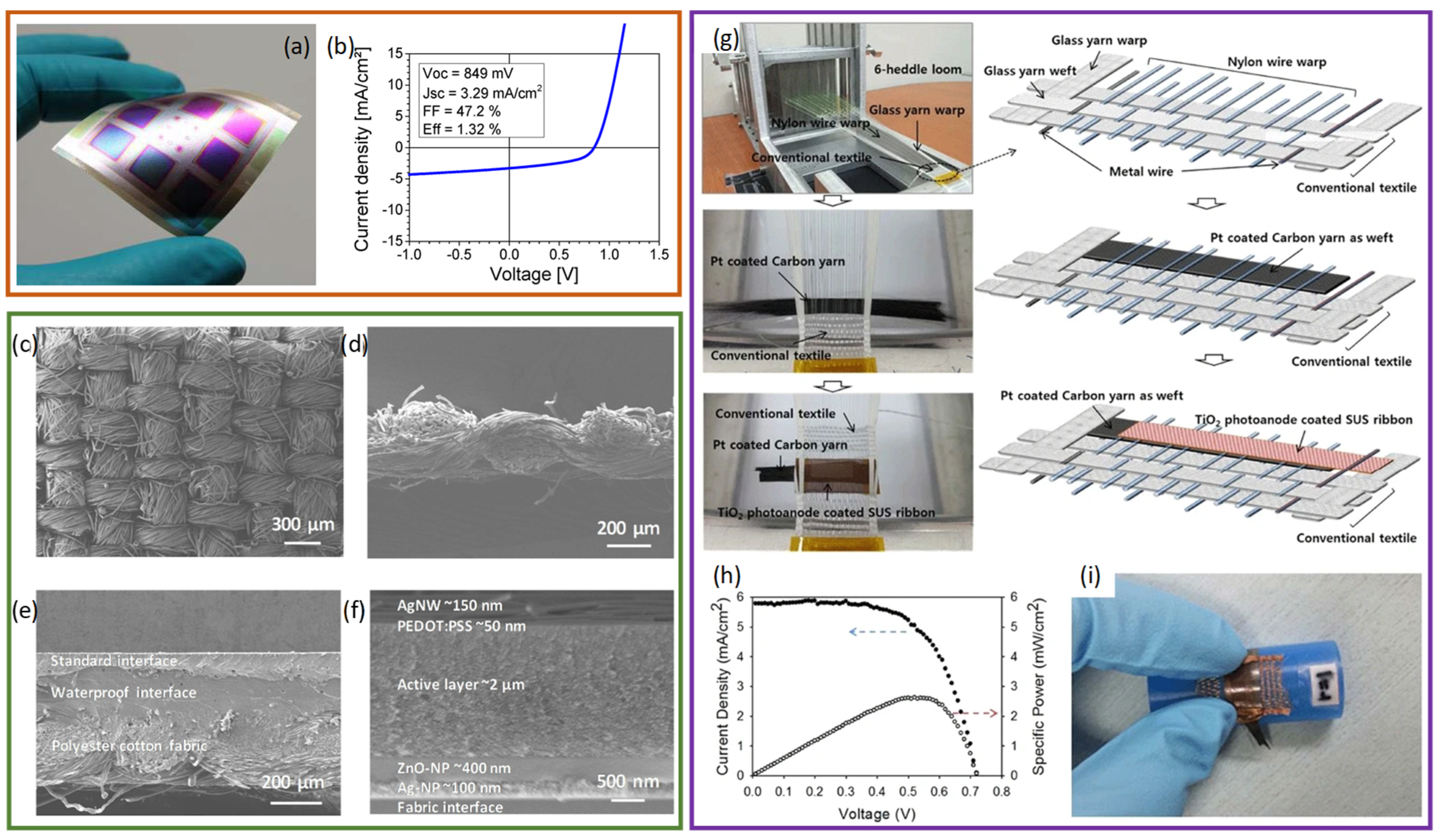
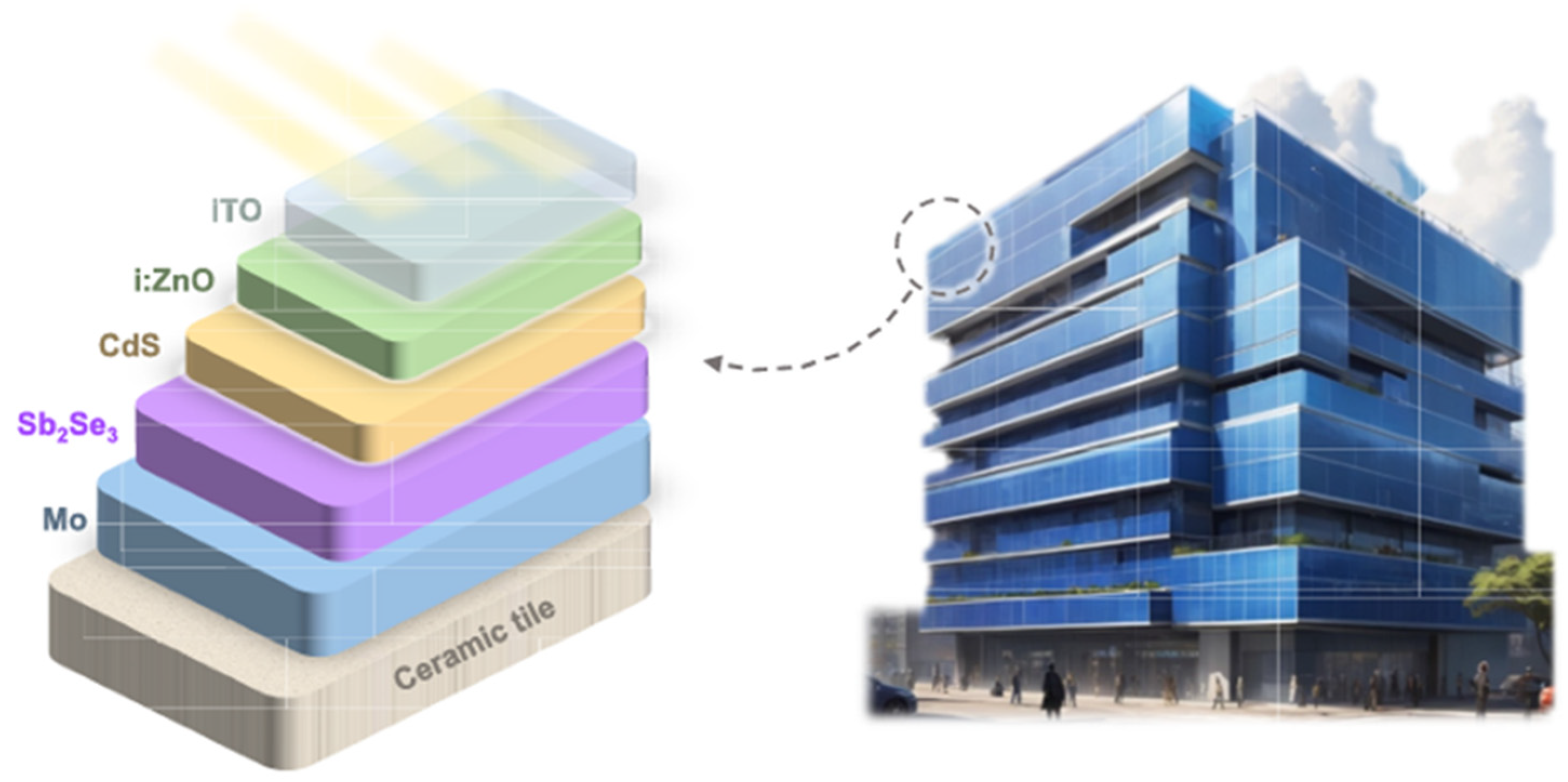
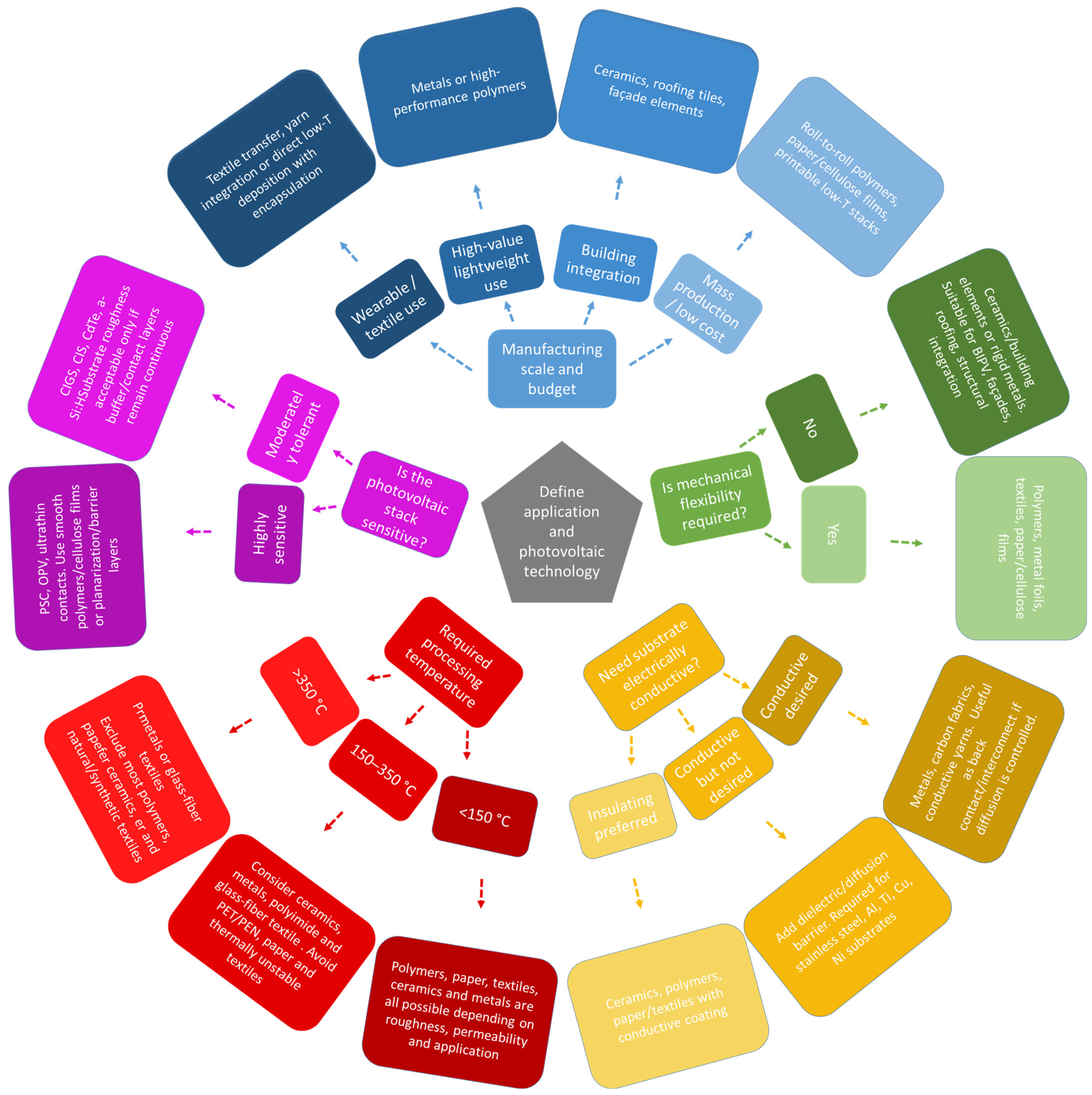
Against this background, the fundamental surface and bulk challenges associated with non-conventional substrates for solar applications are comprehensively reviewed in this work. First, the key physical and chemical limitations inherent to non-conventional substrates are introduced in Section 2, including surface roughness and real-world geometries, ionic diffusion and interfacial contamination, chemical reactivity governing nucleation and adhesion, porosity-related permeability and outgassing phenomena, and thermo-mechanical mismatch affecting device durability. These aspects are discussed as universal constraints that critically influence thin-film deposition, interfacial stability, and long-term photovoltaic performance. Subsequently, the main families of non-conventional substrates employed in solar technologies represented in Figure 1 are systematically analysed in Section 3. Ceramic and building-derived substrates, such as ceramic tiles and roofing elements, are discussed first in Section 3.1, with emphasis on their intrinsic material properties and dominant challenges, including surface roughness, alkali diffusion, porosity, and chemical reactivity. Particular attention is devoted to how these limitations directly force photovoltaic stack design, requiring planarization strategies, glazes, diffusion barriers, interlayers, and strict thermal processing limits, together with representative examples of real solar applications. Metallic substrates are then reviewed in Section 3.2, focusing on their mechanical robustness and flexibility, as well as the dominant issues associated with oxidation, elemental diffusion, electrical short-circuiting, adhesion, and coefficient of thermal expansion (CTE) mismatch, and the corresponding implications for device architecture and interfacial engineering. Polymeric and elastomeric substrates are addressed next in Section 3.3, highlighting their low thermal stability, gas and moisture permeability, outgassing behavior, and surface charge effects, which impose severe constraints on processing temperature, layer compatibility, and long-term stability in flexible photovoltaic systems. Finally, carbon- and bio-derived porous substrates, including paper, textiles, and fibrous carbon materials, are reviewed in Section 3.4, with particular emphasis on their highly porous nature, coating infiltration challenges, mechanical durability, and multifunctional integration potential in emerging solar concepts. Taken together, these sections establish a unified framework linking fundamental substrate-level phenomena with device design constraints across different families of non-conventional substrates, providing a coherent basis for the subsequent outlook, where future research directions and technological opportunities in advanced solar integration are discussed.

2. Fundamental Surface and Bulk Challenges in Non-Conventional Solar Substrates

The facile integration of thin-film solar technology on different types of surfaces has promoted the study of its incorporation on new types of non-conventional substrates [27]. This opens a wide range of possibilities for the development of photovoltaic solar technology in new application fields [4]. Despite this, the impact of the different types of substrates on the device performance and reliability is often addressed in a material-specific manner, although in practice many of the limitations that arise when integrating solar devices on non-conventional substrates are originated from a reduced set of fundamental phenomena that transcend individual substrate classes and different photovoltaic technologies.
In non-conventional substrates, certain properties such as surface roughness across multiple length scales, ionic diffusion from the substrate, chemically active interfaces, porosity-driven mass transport or stresses generated by thermo-mechanical mismatch can trigger effects that become dominantly detrimental for integrated devices [28,29]. This section presents a unified analysis of the fundamental challenges related to the physical and chemical phenomena associated with non-conventional substrates for solar applications, laying the groundwork for a subsequent analysis of the different substrate families in Section 3.

2.1. Roughness, Texture and Real-World Geometries

Surface roughness can be defined as the deviation of a real surface from an ideally flat one, and its impact on photovoltaic devices depends both on the length scale of these deviations and on their relation to the thickness of the functional layers. Table 1 classifies different regimes of deviations and their main effects in solar cell technology.
At the nanometric scale (typically below 10–20 nm), surface roughness primarily influences nucleation behavior, interfacial energetics and defect formation. Local variations in surface energy and curvature modify the density and spatial distribution of nucleation sites, affecting grain size, crystallographic orientation and interfacial recombination in deposited films [30,31]. In thin-film technologies such as chalcopyrite and CdTe solar cells, controlled nanoscale roughness at the substrate or back-contact interface can promote favorable growth modes and enhanced optical absorption without compromising electrical integrity [32,33,34]. In contrast, in photovoltaic devices relying on ultrathin charge-selective layers or mechanically soft semiconductors, including perovskite-based solar cells, even moderate nanometric roughness can induce incomplete coverage, increased trap density and local electric field enhancement, leading to shunting pathways, reduced performance and poor device-to-device reproducibility [35,36].
At submicrometric length scales, surface roughness becomes a dominant factor governing layer continuity and electrical integrity. When the amplitude of surface features approaches or exceeds the thickness of functional layers, local thinning, pinhole formation and electrical short-circuiting become increasingly probable [37,38]. This regime is particularly critical for non-conventional substrates such as ceramics, metals and fibrous materials, where the material and fabrication process can generate roughness at these scales if this issue is not properly anticipated or addressed, as will be discussed in the following sections. This is also the case for emerging transparent conductive layers such as metallic nanowires, which present intrinsic roughness if no planarization techniques are applied [39]. It should be noted that no universal Ra, Rq or Ra/Rq threshold can be defined for the onset of shunting across photovoltaic technologies. Shunting is not governed by an absolute average roughness value, but by the relationship between the local surface-height distribution and the thickness, conformality and electrical function of the layers deposited on top. In particular, local protrusions or peak-to-valley features approaching the thickness of the thinnest electrically critical layer, such as charge-selective layers, buffer layers, transparent electrodes or insulating interlayers, can promote local thinning, pinhole formation and leakage paths. Consequently, roughness tolerance is highly technology- and process-dependent and Ra and Rq should be interpreted as screening parameters rather than universal failure thresholds, and they must be complemented by local defect analysis and cross-sectional verification of layer continuity.
At micrometric length scales, large-amplitude roughness primarily imposes architectural constraints rather than directly disrupting layer continuity. Under these conditions, conventional planar architectures for thin-film solar cells become unviable without the introduction of additional planarization layers or an increase in the thickness of the functional layers, which can result in optical losses, increased series resistance and reduced mechanical flexibility [40].
Larger-scale geometric deviations such as surface waviness or macroscopic curvature can also complicate device integration on non-conventional substrates, generating spatially inhomogeneous performances or increasing mechanical stress concentration [41,42]. This is particularly relevant for flexible and building-integrated photovoltaic systems, where substrate geometry is dictated by architectural or mechanical constraints rather than device optimization. As a result, adapted deposition techniques and specific designs, and in some cases the development of new deposition approaches, are required to ensure conformal depositions and interfacial stability on this surfaces [43].
Taken together, surface roughness, waviness and real-world geometries can impose substrate-specific design requirements if they are not properly mitigated. These constraints manifest differently across substrate families and photovoltaic technologies, as will be illustrated in the subsequent sections dedicated to ceramic, metallic, polymeric and porous fibrous substrates.

2.2. Ionic Diffusion and Interfacial Contamination

Ionic diffusion in photovoltaic devices depends on two main phenomena: on the one hand, thermodynamically favorable driving forces, and on the other, kinetically accessible transport pathways. The magnitude of these phenomena is defined by the nature of the substrate and its interfaces [33]. In non-conventional substrates, diffusion-related phenomena are often amplified due to heterogeneous microstructures, chemically active phases, and reduced control over interfacial chemistry. As a result, ionic migration and interfacial contamination frequently emerge as critical factors limiting both device performance and operational stability.
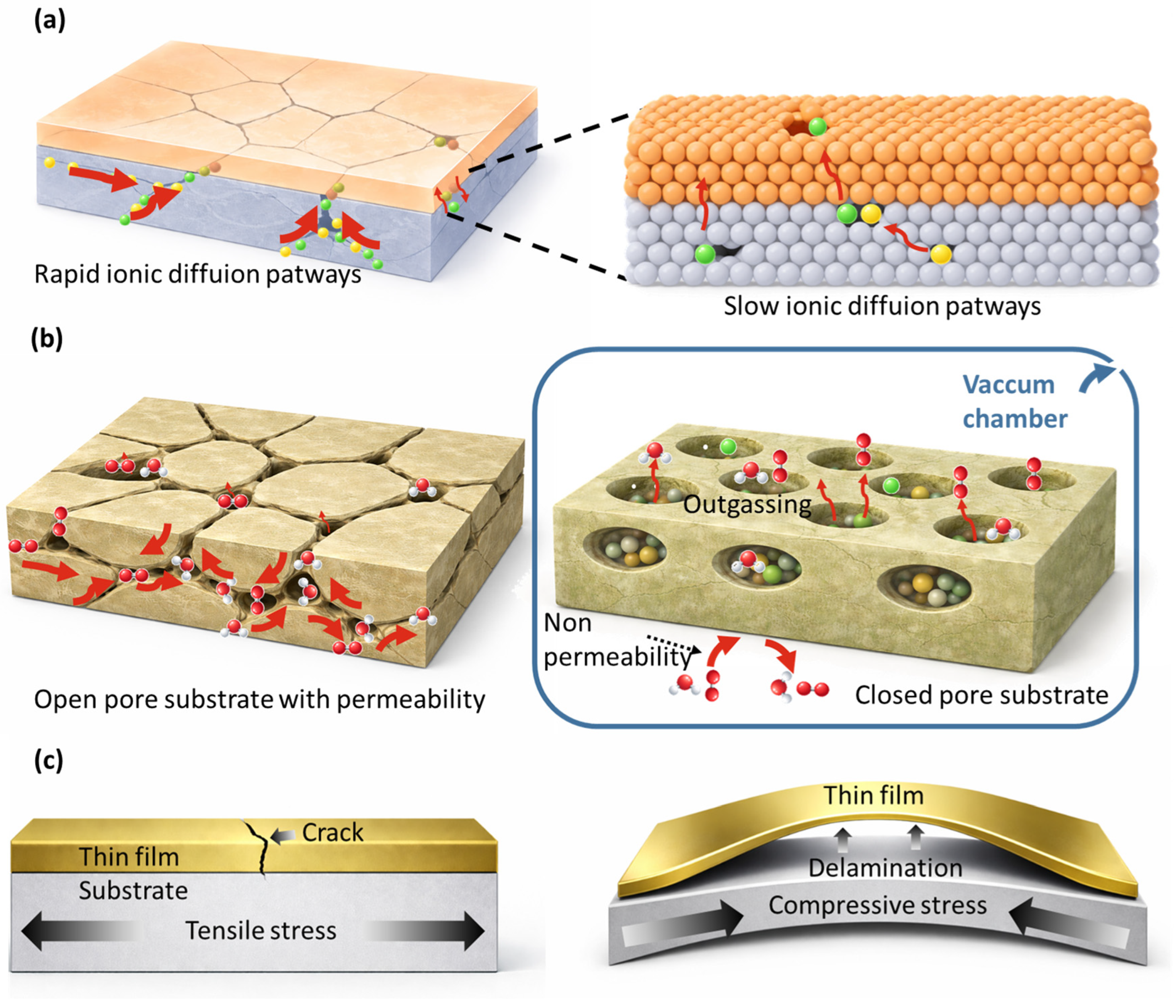
From a physical standpoint, ionic diffusion is driven by chemical potential gradients, electric fields, and temperature [44]. In dense, crystalline substrates, bulk diffusion usually dominates and is characterized by relatively high activation energies. However, in non-conventional substrates, fast diffusion pathways such as grain boundaries, secondary phases, pores as represented in Figure 2a, and interfacial regions often prevail, leading to effective diffusion coefficients several orders of magnitude higher than those predicted solely from bulk properties [45]. This behavior is particularly pronounced in ceramic substrates and building-material-derived substrates rich in alkali elements, as well as in fibrous and porous systems where interconnected void networks facilitate rapid mass transport.
The species involved in substrate-induced diffusion vary widely and include alkali ions (e.g., Na+, K+), alkaline earth elements (e.g., Ca2+), transition metals and, in polymer-based substrates, low-molecular-weight organic compounds [46]. Once mobilized, these species can reach critical interfaces within the photovoltaic stack, where they modify local stoichiometry, induce defect states or participate in redox reactions. In thin-film solar cells such as Copper indium gallium selenide solar cells (CIGS), controlled alkali diffusion can improve grain growth and defect passivation [47]. Conversely, uncontrolled diffusion or the presence of multiple mobile species can lead to secondary phase formation, interfacial degradation and accelerated aging, particularly in chemically sensitive absorber materials [48].
Interfacial contamination represents a closely related but distinct phenomenon, arising from the incorporation of undesired chemical species at buried interfaces during substrate preparation or layer deposition [49]. In non-conventional substrates, surface heterogeneity, porosity and chemical activity increase the likelihood of contaminant retention, including adsorbed moisture, adventitious carbon, organic residues or plasticizers. These contaminants can interfere with nucleation and adhesion, alter interfacial dipoles and introduce electronically active defects that persist throughout device operation [50]. Moreover, contaminated interfaces often act as preferential diffusion pathways, thereby coupling contamination and ionic migration processes.
To mitigate diffusion- and contamination-related degradation, a set of common strategies has emerged across different photovoltaic technologies and substrate families. These include the use of diffusion barrier layers to block mobile species, chemically inert interlayers to decouple reactive substrates from functional layers, and surface treatments aimed at reducing defect density and chemical activity prior to deposition [51,52]. Importantly, the effectiveness of these strategies is constrained by additional factors such as thermal budget, mechanical compatibility and process scalability. Consequently, diffusion-related considerations frequently dictate not only material selection but also the sequence and architecture of the photovoltaic stack.
The impact of ionic diffusion and interfacial contamination therefore extends beyond isolated material issues and constitutes a unifying challenge in the integration of solar devices on non-conventional substrates. The specific manifestations of these phenomena, as well as the mitigation strategies employed, vary substantially across ceramic, metallic, polymeric and porous fibrous substrates, as will be discussed in the following sections.

2.3. Chemical Reactivity, Nucleation and Adhesion

During the first stages of thin film growth, the chemical nature of the substrate surface has a significant impact on the reactivity, nucleation or adhesion of the layers, which also may affect the final morphology and performance of the layer. From a thermodynamic perspective, nucleation and growth are controlled by the balance of surface and interfacial energies, which dictates the preferred growth mode [30]. Depending on the relative values of the substrate surface energy, film surface energy and interfacial energy, thin films may grow in a layer-by-layer (Frank–van der Merwe), island (Volmer–Weber), or mixed (Stranski–Krastanov) mode [53]. In non-conventional substrates, heterogeneous surface terminations and mixed phases present on the surface and residual chemical functionalities can frequently generate a non-uniform nucleation density and island-dominated growth [54]. The effects can have a particular impact on photovoltaic architectures, especially on ultrathin functional layers, where incomplete coverage or delayed coalescence directly translates into electrical losses.
The impact of these interfacial properties in the film growth also varies depending on the deposition mechanism employed as summarized in Table 2. In chemical-governed processes as in deposition techniques based on surface-limited reactions, such as atomic layer deposition (ALD), the absence or low density of suitable surface reactive groups can suppress precursor adsorption or reaction, resulting in non-uniform films, low growth rates during the initial cycles or even complete growth inhibition, and in some cases leading to different film compositions or phases depending on the substrate despite identical process conditions [55,56].
In solution-based deposition methods, surface chemistry plays an even more critical role. Film formation in this case is governed by heterogeneous nucleation and adsorption of precursor complexes from solution, which are highly sensitive to surface charge, acid–base character and local electrostatic environment [57]. The surface zeta potential can strongly influence the adsorption probability of charged species, promoting or suppressing nucleation depending on the sign and magnitude of the surface charge [58]. As a result, substrates with unfavorable surface chemistry may effectively inhibit film growth, even under solution conditions that are optimized for other types of substrates.
On the other hand, in predominantly physical deposition techniques, such as thermal evaporation or sputtering, film growth is mainly governed by the flux, energy and surface mobility of incoming species, with nucleation occurring through physical adsorption and surface diffusion [59]. In this type of technique, substrate chemistry plays a secondary role compared to surface energy, cleanliness and defect density, making these processes generally more tolerant to chemically inert or poorly functionalized substrates. However, limited atom mobility or high defect densities can still promote island-dominated growth and delayed coalescence, which in ultrathin photovoltaic layers may result in incomplete coverage and increased electrical losses [60].
Adhesion is determined from the same physicochemical framework that governs nucleation and interfacial chemistry and will depend critically on the deposition technique employed. In methods with a strong chemical component, such as, solution-based processes, the formation of chemical bonds at the interface generally generates a high adhesion with an enhanced mechanical robustness [61]. In contrast, physical techniques, such as thermal evaporation or sputtering, tend to produce interfaces bounded mainly by physical interactions or mechanical interlocking, which can result in weaker adhesion [62]. Weak or chemically incompatible interfaces can suffer from delamination under thermal or mechanical stress, whereas excessive reactivity can generate interfacial defect states or secondary phases that compromise electronic performance. Such interfacial modifications can also affect the electronic landscape of the device by introducing trap states, modifying local band alignment or generating interfacial dipoles, thereby influencing recombination, charge extraction and leakage behavior.
To address these challenges, interface engineering strategies such as surface activation, chemical functionalization, seed layers or inert interlayers are commonly employed to enhance the surface reactivity and stabilize nucleation behaviour [63]. However, these approaches introduce an addition step and can generate difficulties related to thermal degradation, process compatibility and scalability.

2.4. Porosity, Permeability and Outgassing

The porosity of a material is defined as the ratio between the volume of voids and the total volume of a sample, allowing the empty space contained in a substance to be quantified. In certain substrates such as ceramic tiles, polymers, textiles and fibrous systems, porosity plays a critical role in the mass transport phenomena across photovoltaic devices due to its high presence [64]. These voids can generally be classified into closed porosity (isolated from the external environment) and open or interconnected porosity both represented in Figure 2b, which allows the direct transport of gases, vapors or liquid species through the substrate [65].
The impact of porosity on the long term degradation of photovoltaic devices is directly related to its permeability, which is the property of a porous material that determines how easily a fluid flows through that material [66]. In substrates with open porosity, permeability to environmental species such as oxygen, water vapor or organic molecules can be several orders of magnitude higher than in dense materials [67]. As a consequence, porous substrates can act as transport channels for reactive species, facilitating their diffusion toward the device interfaces and potentially triggering chemical degradation processes, interfacial reactions or dopant redistribution over time [68].
Outgassing, by contrast, is a phenomenon that can have an impact on substrates with both closed or open porosity and arises from the release of volatile species trapped within the substrate during earlier stages. In polymeric and bio-derived substrates, outgassing may involve residual solvents, plasticizers, unreacted monomers or low-molecular-weight degradation products [69]. In porous ceramics tile substrates, adsorbed water, carbonates or processing residues may be released during heating or under vacuum conditions [70]. Once released, these species can contaminate films during growth, interfere with nucleation and adhesion, or generate electronically active defect states at critical interfaces [71].
This porosity-related degradation can limit the use of certain substrates for photovoltaic technologies that are more sensitive to specific types of contamination. Some strategies can also be employed to mitigate the effects of porosity, such as substrate densification, pore sealing or the introduction of barrier layers and encapsulation, which limit the transport of these contaminants at the cost of added process complexity [72,73].
Beyond chemical and interfacial degradation mechanisms, porous substrates can also impose intrinsic thermal limitations. The presence of voids reduces the effective thermal conductivity of the material by disrupting continuous heat conduction pathways and introducing low-conductivity phases (e.g., trapped gases), which increases thermal resistance across the substrate. As a result, this heat dissipation in the substrate can generate a lower surface temperature than the nominal set temperature or exhibit gradients across the substrate thickness. This can affect precursor adsorption kinetics, reaction completeness and nucleation behavior, particularly in temperature-sensitive processes [74].

2.5. Thermo-Mechanical Mismatch and Durability

In completed photovoltaic modules, the difference in the coefficient of thermal expansion (CTE) between photovoltaic devices and the substrate can generate tensile or compressive stresses between them, which can lead to operability problems, affecting device performance both in the short and long term [75,76].
These stresses are usually differentiated into two key stages represented in Figure 2c. First, during processing stages involving high-temperature processes, large thermal variations can generate significant stresses due to CTE differences, leading to immediate failure modes such as crack formation or interfacial delamination [77]. In contrast, under normal device operating conditions, repeated day–night thermal cycles induce lower amplitude stresses but activate fatigue-dominated degradation mechanisms, which lead to the progressive weakening of interfaces and thin functional layers [62,78].
The impact of these stresses will mainly depend on the CTE differences between the substrate and the functional layers, as well as on the relative stiffness of each component of the device. In order to mitigate these differences, conformable interlayers, stress-buffer layers or graded interfaces can be used to redistribute deformation and reduce stress concentration [79,80,81,82]. The proper selection of a substrate with CTE values similar to those of the functional layers can help avoid long term problems of this nature.

3. Families of Non-Conventional Substrates for Solar Applications

3.1. Ceramic and Building-Derived Substrates

3.1.1. Material Properties and Functional Characteristics

Ceramics, glasses, and glass-ceramics share a range of mechanical [83], thermal [84], chemical, and functional properties. In addition, these materials are extensively used in structural and architectural applications [85], refractory components [86], thermal and acoustic insulation systems [87,88], filtration and separation media [89], wear- and corrosion-resistant elements [90], protective coatings [91], electronic devices [92], piezocatalytic applications [93], soft robotics [94] and energy-related technologies, owing to their high durability, chemical stability, and tunable microstructural features.
However, they also exhibit relevant differences arising from their distinct structural characteristics and microstructural nature, which govern their response to mechanical, thermal, and environmental stresses. Table 3 provides a comparative overview of the key properties of these three material classes, highlighting both their commonalities and the critical differences that ultimately define their respective application domains.
Table 3. Properties of ceramics, glasses and glass–ceramics [95].
PropertyCeramics
[96,97]
Glasses
[98]
Glass–Ceramics
[99,100]
Hardness (GPa)10–25 5–9 6–10
Elastic modulus (GPa)100–30060–8080–150
DuctilityLowLowLow
Wear resistanceHigh (qualitative)Moderate–highHigh
Corrosion resistanceHighHighHigh
Chemical resistanceHighHigh (except strong alkali)High
Weather resistanceHighHighHigh
Melting/softening temperature (°C)>1200–1600~600–700 (softening)~800–1200
Thermal expansion (10−6 K−1)3–88–90–5
Thermal conductivity (W·m−1·K−1)1–50.8–1.51–3
Electrical resistivity (Ω·cm)108–10141010–1014109–1013
Tensile strength (MPa)10–10030–9050–150
Compressive strength (MPa)1000–3000500–1500800–2000
Transparency (%)0–10 (opaque)85–920–80 (depends on phase)
Fracture toughness (MPa·m1/2)2–50.7–11–3
Impact strengthLowLowLow–moderate
Thermal shock resistance (ΔT, °C)~100–300~80–150~200–500
Construction materials have historically been dominated by ceramic-based materials [101], primarily due to their high durability, chemical stability, and resistance to harsh environmental conditions [102,103]. These materials form the basis of the building envelope and therefore represent a natural platform for the integration of additional functionalities, such as energy generation [15,104].
In this context, ceramic tiles and roofing tiles are of particular interest for the development of BIPV systems, as they combine widespread deployment in building façades and roofs with large, geometrically well-defined surfaces [105]. The possibility of integrating photovoltaic devices directly on these materials enables building elements to perform a dual function, acting simultaneously as part of the architectural envelope and as electricity generators [16].
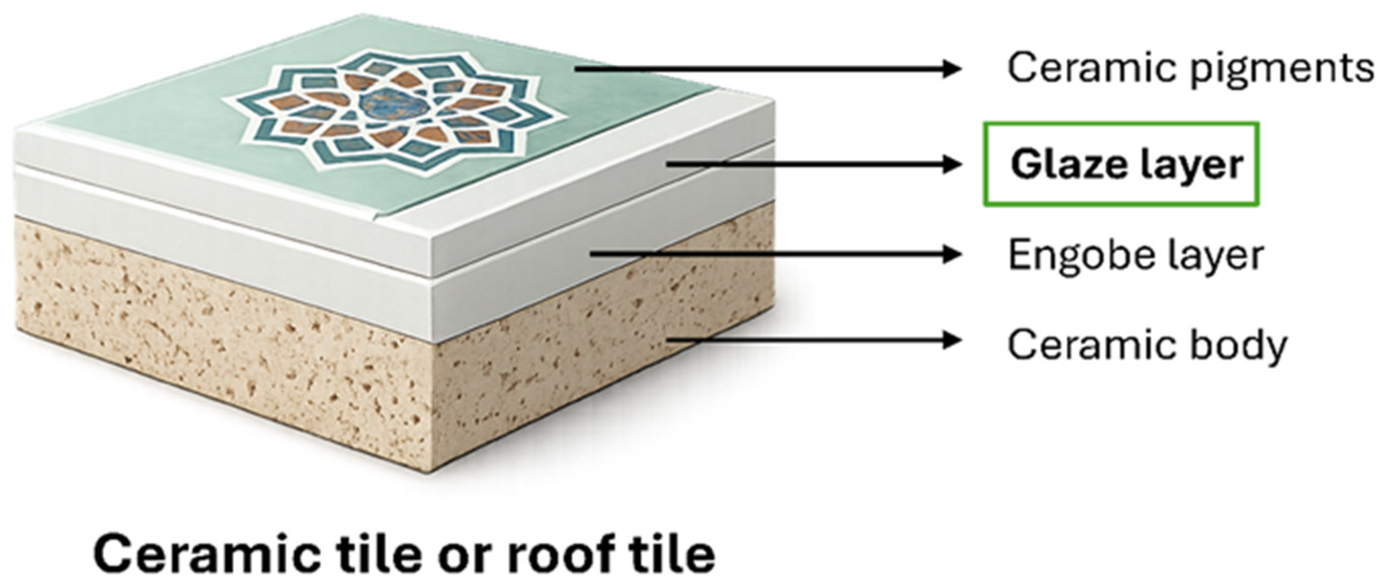
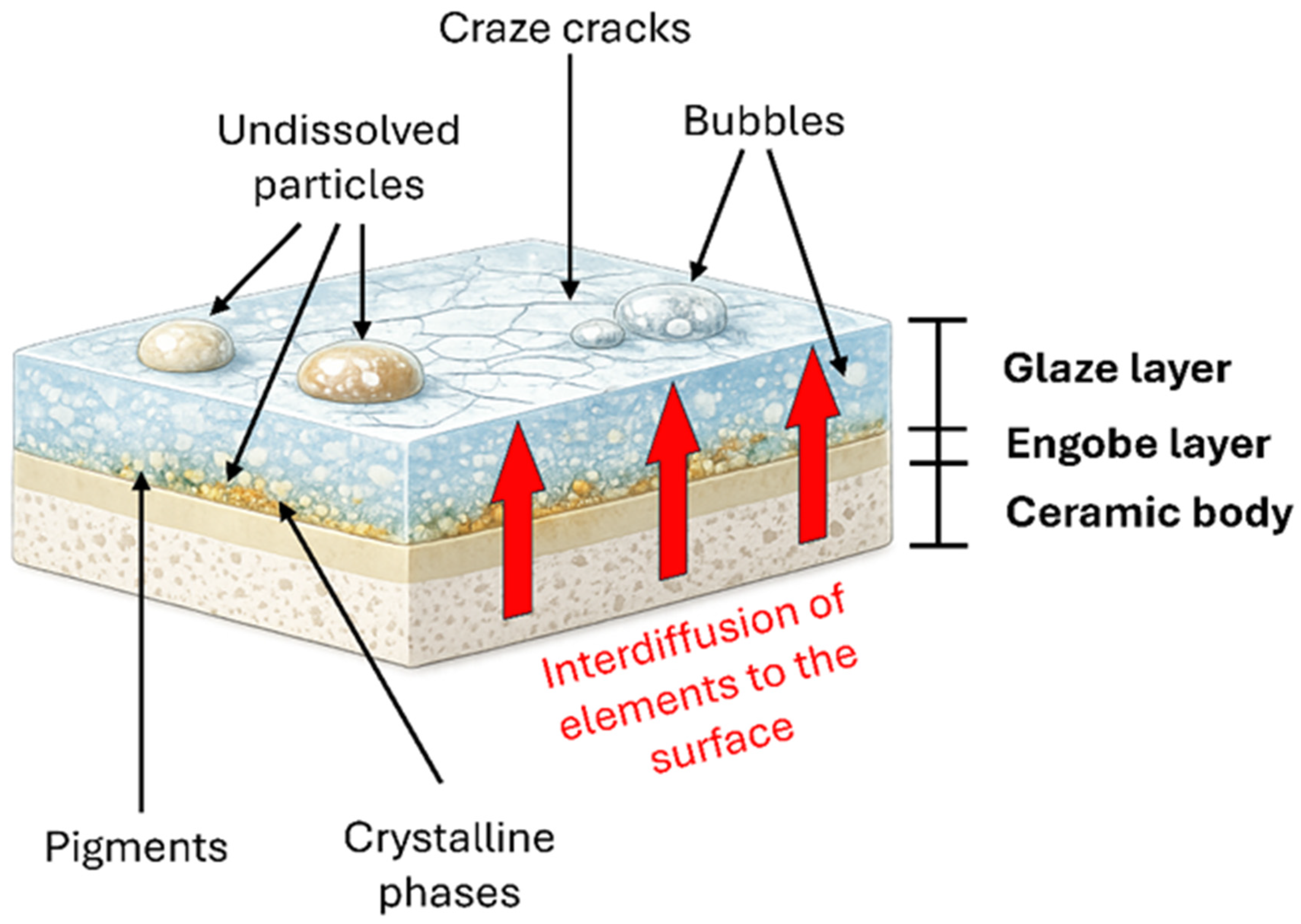
Ceramic tiles and roofing tiles typically consist of a sintered ceramic body mainly composed of aluminosilicate raw materials, including clay minerals (≈30–50 wt.%, e.g., kaolinite and illite), feldspars acting as fluxes (≈35–50 wt.%), and silica in the form of quartz (≈10–25 wt.%), which together provide mechanical strength and dimensional stability [106]. In red ceramic bodies, the characteristic coloration arises from the presence of a minimum content of iron and/or titanium oxides (typically ≥2–3 wt.% Fe2O3, with minor TiO2 contributions), which act as chromophore phases during firing [107]. In many cases, this body is covered by an intermediate engobe layer, composed of aluminosilicate-based materials, which regulates porosity, enhances the enamel adhesion, and adjusts the color of the substrate. Finally, the surface is commonly coated with a vitreous glaze layer, which provides aesthetic properties, protection against chemical and environmental agents, and a functional surface that can be modified or functionalized. This glaze is typically based on a silica-rich glassy matrix (SiO2–Al2O3), fluxed with alkali and alkaline-earth oxides (Na2O, K2O, CaO, MgO) to control melting behavior, and may incorporate zirconia-based opacifiers (ZrO2 or ZrSiO4), as well as minor amounts of transition-metal oxides to tailor optical and functional properties [108]. This stratified architecture, shown in Figure 3, offers multiple interfaces that can be exploited for the integration of active or functional layers in BIPV systems [109].
The glaze layer constitutes the outermost surface, and its characteristics critically determine the properties of the photovoltaic cell fabricated on the surface. A ceramic glaze is a thin vitreous coating that fuses onto the surface of a ceramic body during firing [110]. Unlike glass, a glaze exhibits a high surface-to-volume ratio and undergoes strong interactions with both the ceramic substrate and the kiln atmosphere. While glass can be regarded as an essentially closed system, whose chemical composition remains largely unchanged during thermal treatment, a glaze behaves as an open system, as its composition evolves during firing due to interactions with the ceramic body and the volatilization of specific compounds [111].

3.1.2. Key Challenges: Surface Roughness, Alkali Diffusion, Porosity and Chemical Reactivity

The deposition of a photovoltaic cell onto a glazed surface introduces a set of specific challenges arising from the chemical, microstructural, and functional nature of ceramic glazes [112]. Unlike substrates specifically engineered for electronic applications, ceramic glazes constitute chemically heterogeneous and dynamic systems, whose composition and microstructure are governed by their interaction with the ceramic body during firing [113].
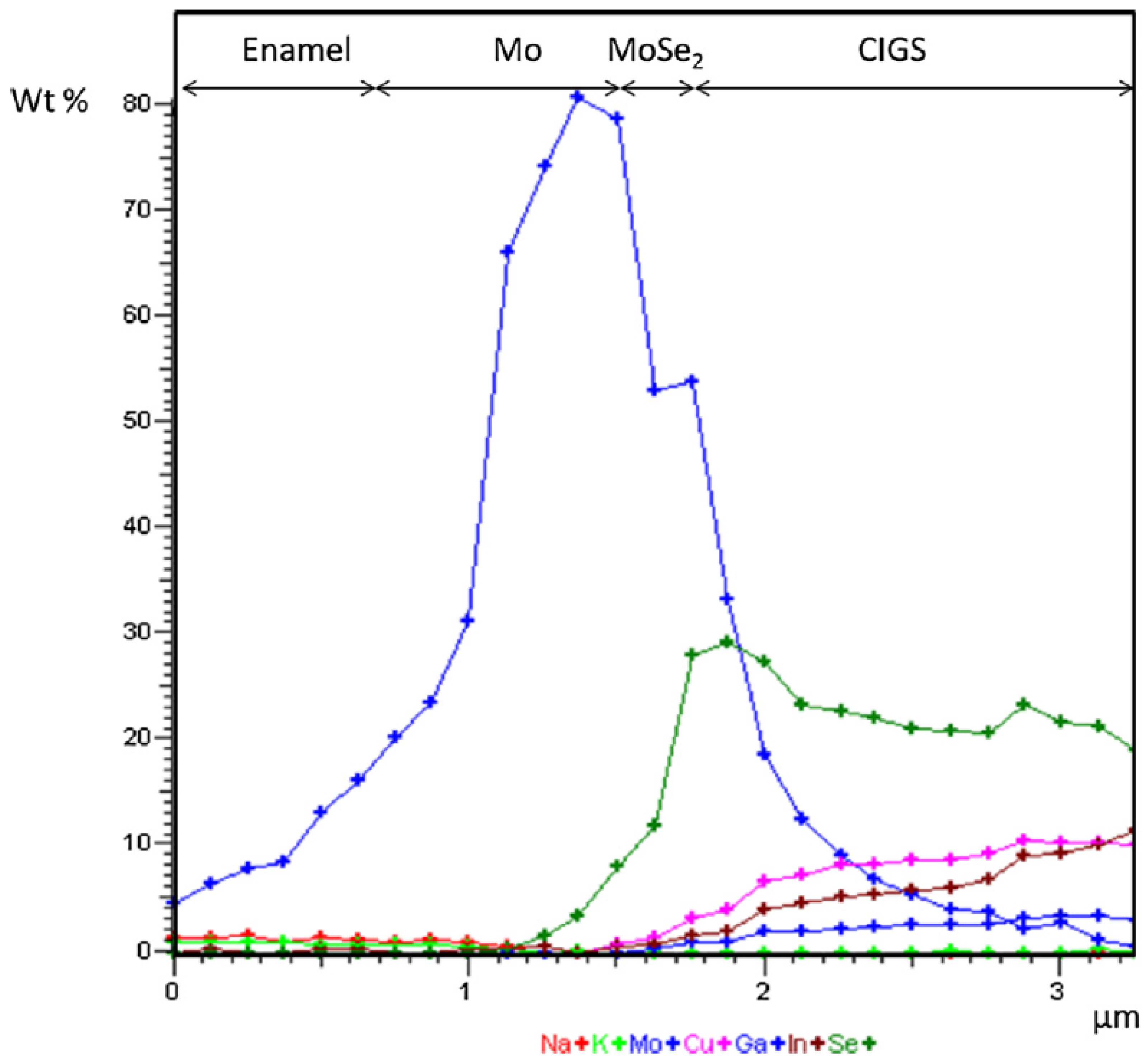
Elemental diffusion across interfaces represents one of the main challenges in the use of non-conventional and glazed ceramic substrates for thin-film photovoltaic applications. In particular, elemental interdiffusion between the vitreous glaze and the ceramic body introduces significant chemical complexity, as demonstrated in previous studies—for example, in the work published by D. Fraga et al. [112], cited here as an illustrative case. That study describes migration processes from the ceramic substrate into the glaze, as well as the diffusion of species originating from pigments embedded in the vitreous matrix, leading to compositional gradients and the formation of chemically complex interfaces as can be seen in Figure 4.
In CIGS-based technologies, the diffusion of alkali elements is likewise a determining factor. Sodium (Na) incorporation has a direct influence on the crystallinity and optoelectronic properties of the absorber layer, and it is widely accepted that Na can diffuse from soda-lime glass substrates during CIGS growth, resulting in beneficial effects on device performance as shown in Figure 4 [114,115]. Nevertheless, despite significant progress, a quantitative understanding of these diffusion processes and the definition of optimal alkali concentrations remain open research challenges.
The presence of undissolved particles, crystalline phases, gas bubbles, and surface microcracking constitutes a set of well-known defects in ceramic glazes, as extensively reported in the specialized literature [116]. These heterogeneities illustrated in Figure 5 introduce topographical irregularities, porosity, and chemical discontinuities that hinder the homogeneous deposition of thin functional layers, increase optical scattering, and compromise the mechanical and chemical integrity of coatings. In photovoltaic applications, such defects adversely affect layer uniformity, device stability, and overall reliability [117].
Overall, these challenges highlight that the use of glazed ceramic surfaces as substrates for photovoltaic cell fabrication requires stringent control over glaze composition, microstructure, and surface state, as well as the implementation of appropriate surface conditioning strategies to ensure the compatibility, stability, and long-term performance of integrated photovoltaic devices.

3.1.3. Impact of Substrate-Related Issues on Photovoltaic Stack Design

For a ceramic support to be suitable for thin-film photovoltaic applications, it must fulfill a set of key requirements, including low porosity high barrier properties, high thermal and chemical resistance, mechanical and thermoelastic compatibility with the functional layers, and industrial viability in terms of cost, reproducibility, and scalability [118]. In this context, the application of industrial vitreous glazes onto the ceramic support plays a fundamental role, as it enables the transformation of an inherently porous and rough surface into a sealed, continuous, and chemically stable interface with a morphology comparable to that of flat glass.
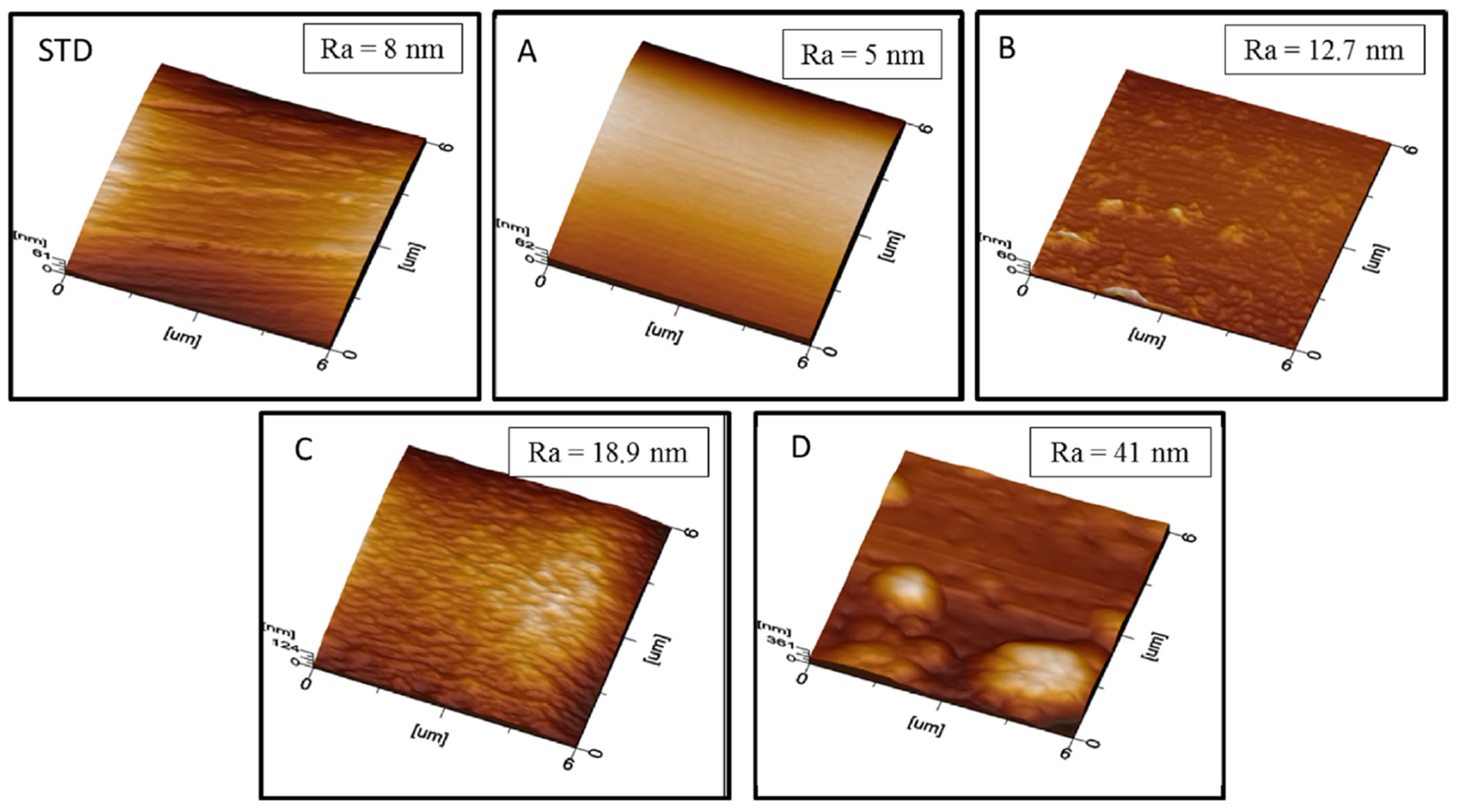
Based on these requirements, a series of glazed ceramic substrates were investigated, using enamel formulations previously reported in the literature [112]. The study started with a standard enamel (STD) with the minimum alkali content required to ensure adequate physical and chemical properties. From this reference composition, glazes with progressively increasing alkali contents were designed by primarily adjusting the Na2O concentration, while compensating with K2O to maintain industrially viable formulations, as summarized in Table 4. The total alkali content (Na2O + K2O) was kept below 8% to avoid surface defects, in accordance with literature reports.
The surface morphology of the enamelled substrates was analyzed by AFM (Figure 6), revealing a clear correlation between alkali content and surface roughness. Samples STD and A exhibited the smoothest and most homogeneous surfaces, with low roughness values (Ra = 8 and 5 nm, respectively). As the alkali content increased, surface roughness progressively rose, as observed for samples B and C (Ra ≈ 13 and 19 nm), due to the appearance of surface heterogeneities. Sample D, with the highest alkali content, showed a markedly irregular morphology characterized by large crystalline features and a significantly higher roughness (Ra = 41 nm).
Overall, these results demonstrate the existence of an optimal alkali content window that allows the formation of smooth, homogeneous glazed surfaces compatible with the uniform deposition of thin-film photovoltaic layers.
In another work by S. Porcar et al. [104], the enamel onto which an Sb2Se3 solar cell was deposited presented a final composition expressed as oxide weight percentages, using 2 wt.% Na2O and 4.6 wt.% K2O. The complete formulation consisted of 7.3 wt.% Al2O3, 8.5 wt.% CaO, 11.7 wt.% ZnO, 62.3 wt.% SiO2, and less than 1 wt.% of other oxides, such as MgO, TiO2, and B2O3 [47].
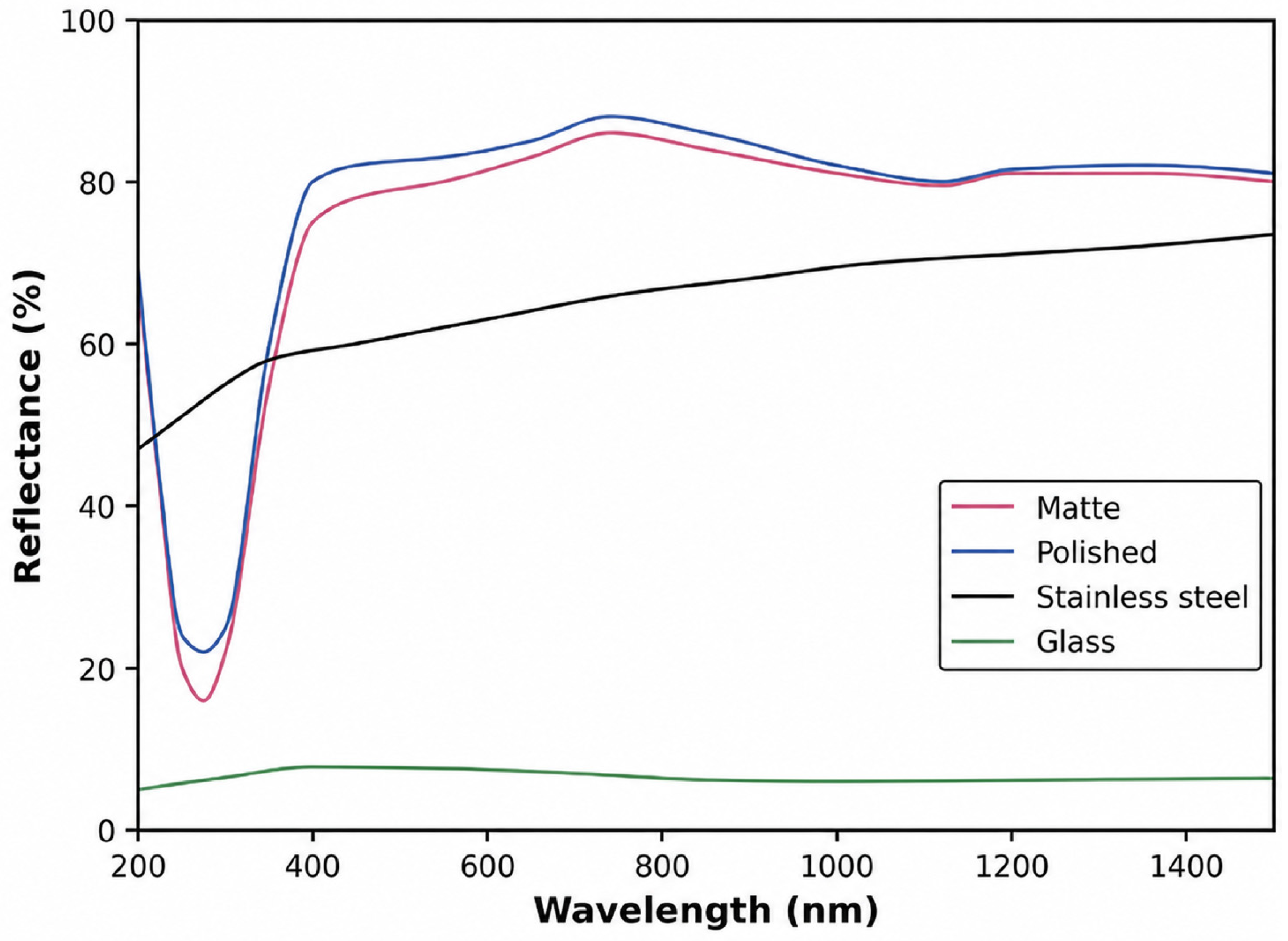
In addition to the chemical composition, another relevant aspect of the ceramic enamel is its surface roughness, which is generally associated with either a matte or a polished finish. Polished ceramic enamels tend to present flatter surface topography while matte enamels typically present partially unfused particles at the surface, which are responsible for the characteristic matte appearance. This parameter is critical in the fabrication of thin-film photovoltaic cells, as higher roughness directly affects the nucleation, growth, and continuity of the functional layers, as well as the final electrical properties of the device. From an optical standpoint, reflectance characterization reveals that both surface finishes exhibit very similar behavior. As shown in Figure 7, matte and polished ceramic enamels display a high total reflectance close to 80% across most of the visible and near-infrared regions. The slight differences observed between the two finishes are consistent with the fact that the main morphological variations occur at length scales of several tens of micrometers, which are too large to interact significantly with visible wavelengths. In the ultraviolet region, both enamels show a pronounced decrease in reflectance, reaching values on the order of 20–25% around 300 nm. Compared to reference substrates such as glass and stainless steel, ceramic enamels exhibit a clearly higher reflectance over the entire spectral range, which may enhance back-reflection of the incident radiation and potentially contribute to increased optical absorption in the photovoltaic active layer [15].
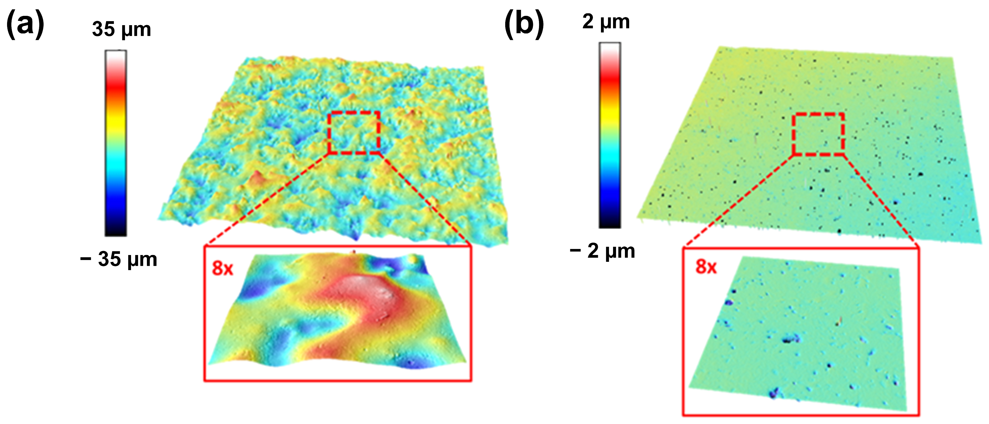
Confocal microscopy observations, as shown in Figure 8, reveal the presence of local surface defects, mainly pores and pinholes originating from the ceramic sintering process, even on polished surfaces (Figure 8b). Despite their presence, the defect density remains sufficiently low to enable continuous layer deposition without macroscopic discontinuities, as such defects are difficult to completely eliminate in ceramic enamels. Although these imperfections could potentially hinder thin-film solar cell fabrication, previous studies on stainless steel substrates have demonstrated that this level of surface imperfection is tolerable for CIS growth [119]. Polished substrates (Figure 8b) exhibit a smoother and more homogeneous morphology than matte ones (Figure 8a). In both cases, pinholes and localized crystallization features are observed, albeit more frequently on matte enamels. Overall, the void density is low, as expected for ultra-compact sintered ceramic substrates of this type.
The photovoltaic comparison reported by Delgado-Sánchez et al. [15] provides a useful example of how ceramic surface finishing affects CIS device performance without preventing successful device operation. In that study, CIS solar cells fabricated on glazed ceramic enamels with polished and matte finishes reached efficiencies of 5.8% and 5.5%, respectively, close to the 6.1% obtained for the reference device on glass. The polished ceramic substrate performed slightly better than the matte one, consistent with its smoother and more homogeneous surface morphology.
The main difference between the ceramic and glass devices was associated with the fill factor rather than with the short-circuit current density. The glass-based device exhibited a FF of 53.6%, whereas the values obtained on polished and matte ceramic substrates were 48.3% and 44.6%, respectively. By contrast, Jsc remained very similar for all substrates, around 29–30 mA cm−2, indicating that the ceramic surface did not strongly limit optical absorption or photocurrent generation. The open-circuit voltage was slightly higher for the ceramic-based devices, with values above 400 mV compared with 392 mV for the glass reference, which was attributed to alkali diffusion from the ceramic substrate into the CIS absorber and its potential contribution to grain-boundary passivation and reduced recombination losses.
Overall, these results indicate that although ceramic surface roughness and localized defects affect interfacial homogeneity and certain electrical parameters, properly finished ceramic enamels can still support continuous CIS layer deposition and functional thin-film photovoltaic operation. This confirms the suitability of polished and matte glazed ceramic substrates for BIPV-oriented CIS solar cells, provided that surface conditioning and defect control are adequately addressed.

3.1.4. Representative Examples of Solar Integration on Ceramic Substrates

Table 5 summarizes representative examples of photovoltaic integration on ceramic substrates reported in the literature, highlighting the evolution of device performance and technological maturity. Early studies demonstrated the feasibility of directly depositing thin-film photovoltaic stacks on glazed ceramic tiles, although with relatively low efficiencies. For instance, Calvet et al.reported CZTSSe solar cells on ceramic substrates with efficiencies around 2% [46], while Oliveira et al. achieved 3.1% efficiency for Cu(In,Ga)(S,Se)2 devices synthesized by in situ sol–gel processing [46,120].
Subsequent works focused on chalcopyrite absorbers, showing progressive improvements. Fraga et al. [112] demonstrated that optimizing the alkali content of the ceramic enamel (4 wt.% Na2O and 3.2 wt.% K2O) enabled CIGS solar cells with efficiencies up to 3.5%. Similarly, Delgado-Sánchez et al. [15] reported stable CIS devices directly deposited on glazed ceramic tiles, reaching efficiencies of approximately 5.5%, confirming the electrical and thermal compatibility of ceramic substrates without the need for barrier layers. Moving into amorphous silicon (a-Si:H), Águas et al. reported the fabrication of a-Si:H solar cells directly deposited onto glazed ceramic tiles, achieving power conversion efficiencies of up to ~5% [121].
More recent studies extended ceramic integration to emerging absorbers. Porcar et al. [104] reported Sb2Se3 solar cells on ceramic enamels with efficiencies of 2.13%, demonstrating the versatility of ceramic substrates across different photovoltaic technologies (architecture of the cell in Figure 9).
Notably, the highest efficiencies reported on ceramic substrates to date have been achieved by Bosio et al. [122], who fabricated CIGS-based solar cells on glazed ceramic tiles with efficiencies reaching 14.28%, approaching those obtained on conventional glass substrates. This result clearly demonstrates that, with appropriate substrate engineering and process optimization, ceramic substrates can support high-performance thin-film photovoltaic devices.
Overall, the studies summarized in Table 6 confirm the technological viability of ceramic enamels as robust, multifunctional substrates for photovoltaic integration, particularly in the context of building-integrated and architectural photovoltaic applications.
Table 5. Representative examples of thin-film photovoltaic devices integrated on ceramic substrates and their reported efficiencies.
Reference (Year)PV TechnologySubstrateMain Result
Porcar et al. (2024) [104]
  • Ceramic enamel
  • Mo
  • Sb2Se3
  • CdS/ZnO
  • ITO
Glazed ceramic tileEfficiency of 2.13% in Sb2Se3 solar cells on ceramic substrates
Delgado-Sánchez et al. (2020) [15]
  • Ceramic enamel
  • Mo
  • p-CuInSe2
  • n-CdS
  • Al:ZnO
Glazed ceramic tileCIS cells directly on ceramic; stable electrical response; device efficiencies of 5.5%
D. Fraga et al. (2018) [123]
  • Glass-ceramic
  • Mo
  • CuIn0.7Ga0.3Se2
  • CdS
  • i-ZnO
  • ITO
Glass-ceramic containing industrial wasteCIGS solar cells with device efficiencies of 0.4%
Fraga et al. (2017) [112]
  • Ceramic enamel
  • Mo
  • CuIn0.7Ga0.3Se2
  • CdS
  • i-ZnO
  • ITO
Glazed ceramic tileThe optimal alkali content (4 wt% Na2O and 3.2 wt% K2O) yields a CIGS solar cell efficiency of 3.5%.
Calvet et al. (2015) [46]
  • Ceramic enamel
  • Mo
  • CZTSSe
  • CdS
  • i-ZnO
  • ITO
Glazed ceramic tileCZTSSe photovoltaic ceramic tile achieving 2% efficiency on ceramic substrate.
Oliveira L. et al. (2013) [120]
  • Ceramic enamel
  • Mo
  • Cu(In,Ga)(S,Se)2
  • CdS
  • i-ZnO
  • ZnO:Al
Glazed ceramic tileCu(In,Ga)(S,Se)2 devices achieved 3.1% efficiency.
Águas et al. (2011) [121]
  • tile/ceramic tile
  • back contact
  • na-Si:H
  • i-pm-Si:H
  • p-nc-Si:C:H
  • p-a-Si:C:H
  • front contact
Glazed ceramic tilea-Si:H solar cells achieving efficiencies near 5%.
Bosio et al. (2014) [122]
  • Ceramic enamel
  • Mo
  • Cu(In,Ga)(S,Se)2
  • CdS
  • i-ZnO
  • ITO
Glazed ceramic tileHighest efficiencies reported on ceramic substrates 14.28%.
Table 6. Key properties of metallic materials for photovoltaic substrates.
PropertyStainless SteelAluminumTitaniumNickelCopperInconel (Ni–Cr)
Density (g·cm−3)~7.9~2.7~4.5~8.9~8.9~8.4
Thermal expansion coefficient (10−6 K−1)16–17~238–9~13~1713–15
Elastic modulus (GPa)~200~70~110~200~110~210
Corrosion resistanceVery highMediumVery highMediumLow–MediumVery high
Chemical resistanceHighMediumVery highMediumMediumVery high
Melting point (°C)~1400~660~1668~1455~1085>1300
Thermal conductivity (W·m−1·K−1)~15~235~22~90~400~11
Tensile strength (MPa)500–100070–300300–900400–700200–400800–1200
Thermal shock resistanceHighMediumHighMediumLow–MediumHigh

3.2. Metallic Substrates

3.2.1. Material Properties and Functional Characteristics

The use of metallic substrates in photovoltaic cells has attracted increasing interest in the development of next-generation solar devices, particularly in the context of thin and flexible modules [124]. Such configurations enable advanced applications in sectors such as space [125], aeronautics [126], and mobile systems, where low weight, mechanical flexibility, and structural robustness are critical requirements [127].
In recent years, significant efforts have been devoted to the development of lightweight and flexible photovoltaic modules based on thin-film technologies. These advances have been driven by the high efficiencies achieved at small scale on both polymeric and metallic substrates [128]. Within this framework, a wide range of substrates has been investigated, with flexible metal foils standing out due to their combination of thermal stability, compatibility with vacuum-based processing, and the high reliability of the resulting devices [129,130].
Among the various metals studied, stainless steel foils are considered one of the most viable options from an industrial perspective. Their attractiveness stems from their relatively low cost, large-scale availability, and particularly their coefficient of thermal expansion, which is comparable to that of the typical multilayer stack of thin-film photovoltaic devices. This thermal compatibility reduces mechanical stresses during fabrication and operation, thereby contributing to enhanced stability and durability of the final device [131].
Table 6 summarizes the main physical, mechanical, thermal, and chemical properties of several metals and alloys commonly used or investigated as photovoltaic substrates. The comparison highlights the trade-offs between low density, high thermal and chemical stability, and high-temperature capability. This overview provides a practical basis for selecting suitable metallic substrates depending on the photovoltaic technology and the targeted application.

3.2.2. Challenges Associated with Metallic Substrates

The development of solar cells on metallic substrates is constrained by a number of technical challenges that must be addressed in an integrated manner to ensure both device efficiency and long-term stability [132]. The most critical requirement is the electrical insulation of the substrate, since metals such as stainless steel, aluminum, or titanium are intrinsically conductive [133]. Consequently, dielectric layers—such as ceramic oxides (Al2O3, SiO2) or nitrides (AlN)—must be introduced to provide effective electrical isolation while maintaining good adhesion and thermal stability within the photovoltaic stack [134]. In contrast, high-purity molybdenum foil offers a distinct advantage, as it can be directly used as a back contact without additional barrier layers [135]. Unlike stainless steel substrates, which often contain deep-level impurities such as Fe that may diffuse into the absorber and degrade its electronic properties, molybdenum foil minimizes contamination-related losses and simplifies the device architecture.
Once electrical insulation is ensured, controlling the diffusion of elements from the metallic substrate into the functional layers becomes one of the main limiting factors [136]. In stainless steel substrates, for instance, the diffusion of Fe, Cr, or Ni into absorbers such as Cu(In,Ga)Se2 can modify their electronic properties and degrade device performance. Similarly, in Cu substrates or Ni-based alloys, the migration of metallic species during thermal treatments necessitates the use of dedicated diffusion barrier layers, such as Mo, TiN, or oxide/nitride multilayer structures, to preserve the chemical integrity of the photovoltaic device [137].
Thermal compatibility between the metallic substrate and the functional layers also represents a key challenge [138]. Metals such as aluminum exhibit relatively high thermal expansion coefficients [139], which can induce significant mechanical stresses during processing or operation. In contrast, materials such as titanium or Ni–Cr alloys offer improved thermal matching with semiconductor and ceramic layers [140]. If not properly managed, these stresses can lead to cracking or delamination, directly affecting device reliability.
In addition, the surface roughness inherent to many metallic substrates poses a challenge for the uniform deposition of thin films [36]. Substrates such as rolled stainless steel or flexible metal foils often require surface polishing, controlled texturing, or leveling layers to enable homogeneous growth of the photovoltaic layers. Finally, the chemical stability and corrosion resistance of the metallic substrate are essential, particularly for long-term operation or exposure to harsh environments, where materials such as stainless steel or superalloys present clear advantages over more reactive metals [141].

3.2.3. Barrier Layers and Interface Engineering

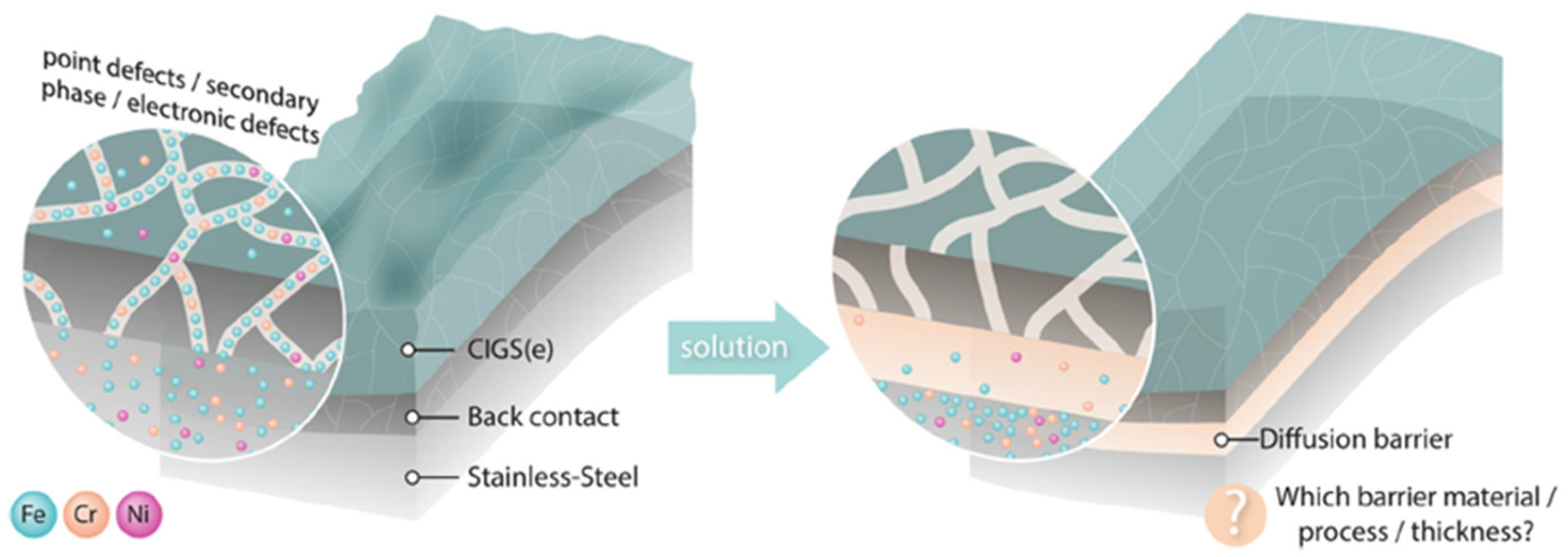
In thin-film photovoltaic technologies fabricated on metallic substrates, diffusion barriers are essential to decouple the chemical nature of the substrate from the functional layers of the device [142]. While metallic substrates provide mechanical robustness and thermal stability, they also act as reservoirs of metallic impurities that can diffuse into the photovoltaic stack during high-temperature processing. As a result, impurity containment and stack isolation become critical requirements for achieving stable and high-efficiency devices [143].
This issue is particularly severe when semiconductor absorbers are grown on stainless steel substrates. Stainless steel is primarily composed of Fe, Cr and Mn, which together account for more than 90% of its chemical composition [144]. These elements—especially iron—are known to have a detrimental impact on absorber materials, as they can act as deep electronic defects or form secondary phases. Even relatively low iron concentrations have been shown to reduce charge carrier collection, particularly in the near-infrared region, while also decreasing the effective doping density and carrier mobility [145]. At higher concentrations, parasitic compounds such as CuFeSe2 or Fe-based chalcogenides may form, severely compromising absorber functionality. To reach high-efficiency thin-film solar cells, impurity concentrations must therefore be reduced to extremely low levels, in some cases approaching sub-ppm thresholds.
Once metallic impurities penetrate the absorber layer, their impact is difficult to reverse. Diffusion kinetics in thin-film absorbers often lead to a rapid and nearly uniform distribution of impurities across the film thickness, effectively degrading the entire layer. Consequently, preventive strategies based on diffusion barriers are essential. These barriers are placed between the metallic substrate and the back contact or absorber to block impurity migration while maintaining adhesion, thermal stability and compatibility with subsequent processing steps [146].
Figure 10 schematically illustrates this concept. On the left side, the absence of a diffusion barrier allows metallic species originating from the stainless steel substrate to migrate through the back contact and into the absorber. These impurities accumulate within grains and at grain boundaries, where they induce point defects, secondary phases and electronic traps that degrade device performance. On the right side, the introduction of a diffusion barrier effectively confines these metallic species to the substrate region, preserving the chemical purity and electronic quality of the absorber layer. The figure also emphasizes that the effectiveness of this approach depends critically on the choice of barrier material, deposition process and thickness, which must be carefully optimized to ensure robust diffusion blocking without introducing additional mechanical or electrical penalties.

3.2.4. Representative Studies from the Literature

Metallic substrates have been widely investigated in thin-film photovoltaic technologies due to their mechanical flexibility, thermal robustness, and compatibility with large-area fabrication processes. Among them, stainless steel (SS) has been extensively used as a flexible substrate for CIGS solar cells, typically requiring dielectric and metallic interlayers to ensure electrical insulation and suitable back-contact properties. For instance, CIGS devices fabricated on stainless steel substrates incorporating SiO2 and Mo layers have achieved power conversion efficiencies of up to 12.6% [147].
Aluminum foil has also been explored as a lightweight and low-cost metallic substrate for CIGS solar cells. In this case, conductive oxide layers such as FTO are commonly introduced to provide chemical insulation between the aluminum substrate and the active device stack. Using this approach, CIGS solar cells deposited on aluminum foil substrates have demonstrated efficiencies around 6.6% [148], highlighting both the potential and the limitations associated with aluminum-based supports.
In contrast, high-purity molybdenum foil offers distinct advantages, as it can act simultaneously as a flexible substrate and an effective back contact, eliminating the need for additional barrier layers. This simplified architecture has been successfully applied to kesterite CZTS solar cells, where devices fabricated on molybdenum foil substrates reached efficiencies of 3.82% [149]. Although the reported efficiencies are lower than those of CIGS devices, this approach demonstrates the feasibility of streamlined device designs enabled by chemically stable and impurity-free metallic substrates.
Table 7 provides an overview of these representative studies, including the corresponding device architectures, substrate types and reported power conversion efficiencies, in the “Overview of photovoltaic devices fabricated on metallic substrates” below.
Table 7. Overview of photovoltaic devices fabricated on metallic substrates.
(Year) ReferencePV StructureSubstrateConversion Efficiency
Y. Kawano et al. (2020) [147]
  • SS
  • SiO2
  • Mo
  • CIGS
  • CdS
  • ZnO
  • ITO
Stainless steel (SS)12.6%
D. Brémaud et al. (2007) [148]
  • Al Foil
  • FTO
  • Mo
  • CIGS
  • CdS
  • AZO
Al6.6%
Y. Zhang et al. (2014) [149]
  • Mo foil (flexible substrate)
  • Mo film
  • CZTS
  • CdS ZnO
  • Al:ZnO
Mo3.82%
T. Yagioka et al. (2009) [130]
  • Ti Foil
  • Mo
  • CIGS
  • CBD-ZnS(O, OH)
  • ZnO:Al
Ti17.9%
L. Wei et al. (2025) [136]
  • Ni foil
  • NiOx
  • Ph-4PACz
  • Perovskite
  • C60
  • BCP
  • ITO
Ni11.42%
B. Abdollahi Nejand et al. (2016) [150]
  • Cu
  • CuI
  • CH3NH3PbI3
  • ZnO
Cu12.80%
Miettunen, K. et al. (2010) [151]
  • Inconel (Ni–Cr)
  • Porous TiO2
  • N719 dye
  • Liquid electrolyte (I−/I3−)
  • Pt
  • FTO
Inconel (Ni–Cr)2.8%

3.3. Polymeric and Elastomeric Substrates

Elastomeric and/or polymeric substrates are of great importance due to their mechanical flexibility, weight, and compatibility with low-temperature synthesis. Because of these characteristics, they are optimal substrates for the deposition of functional layers using sol–gel techniques or mild chemical processes, facilitating the fabrication of photovoltaic layers or devices on curved or other portable shapes and surfaces [4].
These substrates offer advantages over others, such as ceramics or metals, in that they strike a good balance between thermal stability, environmental sensitivity, and mechanical deformation. New forms of application have emerged thanks to characteristics of these materials, such as low density and high flexibility. However, their molecular composition imposes limitations in terms of processing temperature, gas and water vapor permeability, heterogeneous surface charge, and less robust durability compared to other materials. These constraints reflect fundamental challenges at the surface and volume levels, which are discussed in previous sections (Section 2), and they influence the stability and design of flexible photovoltaic devices [4,152].
Polymeric materials are easily produced using continuous roll-to-roll (R2R) manufacturing, where flexible sheets are produced in an assembly line and sequentially coated with functional layers in a continuous process. This type of manufacturing provides high scalability for flexible photovoltaic devices and printed electronics, giving these composite materials clear potential. The ease of integrating these polymeric materials in R2R processes with organic, hybrid, and thin-film semiconductors has driven the development of flexible and lightweight photovoltaic technology [4,153,154,155].

3.3.1. Fundamental Properties and Representative Materials

In the field of flexible photovoltaics, the most studied materials are polyimides (CPIs), naphthalate (PEN) and terephthalate (PET). PET and PEN are the least expensive, with good optical transparency and adequate ductility, consistent with flexible devices. These characteristics are combined with a low glass transition temperature (70 °C for PET and 120 °C for PEN), limiting their use in high-temperature industrial manufacturing processes. In contrast, CPI have better thermal stability, exceeding 300 °C for the glass transition, and high mechanical and chemical resistance. For these reasons, these materials are the most commonly used substrates in the study of flexible photovoltaic devices, as they are more tolerant of high temperatures [154,156]. Table 8 below shows some of the most important characteristics of these materials.
There are other elastic materials, such as thermoplastic polyurethanes (TPU) or polydimethylsiloxane (PDMS), that are used as intermediate layers, due to their viscoelastic behavior, thus redistributing mechanical stresses during bending, reducing potential cracks or delamination in thin or ultrathin layers and improving the mechanical durability of the entire material [157,158].

3.3.2. Thermal Limitations and Processing Strategies

The main limitation of most elastomeric materials is their low thermal adaptability. Traditionally, photovoltaic technologies rely on crystalline silicon or thin films based on CIGS, CdTe (cadmium telluride), or a-Si:H (amorphous hydrogenated silicon), which are highly thermally tolerant materials compared to more common materials. For this reason, the elastomers or polymeric substrates used in photovoltaics must be able to operate at low temperatures; perovskite or organic solar cells fall into this category [4,159].
To overcome these limitations, low-temperature manufacturing strategies are commonly used, including plasma-assisted deposition, solution processing, and other mild-chemistry methods that allow for maintaining the dimensional stability and mechanical integrity of an elastomeric material. The focus of these studies highlights that the substrate imposes thermal constraints, prompting the investigation of new, viable processing routes for these flexible photovoltaic systems [4].
Thin-film polymeric substrates for photovoltaic technology are becoming increasingly relevant, particularly in inorganic systems processed at low temperatures. One example is Sb2Se3-based solar cells, where the possibility of using elastomeric systems, such as polyimides, alongside conventional materials like metal sheets or glass has been explored. However, this highlights that while these materials are viable to process, they have limitations in terms of temperature, lifespan, and surface resistance. Current research is exploring alternative substrates, such as ceramic materials, which significantly overcome these limitations and can facilitate their integration into urban building models [104].
Representative experimental examples illustrating the integration of thin-film photovoltaic devices and low-temperature-compatible processes on polymeric, elastomeric, or related flexible substrates are summarized in Table 9.
Table 9. Experimental studies on photovoltaic devices and processes associated with polymeric and elastomeric substrate integration.
Reference (Year)Photovoltaic Technology/ProcessSpecific Polymer or Substrate TypeMain Relevance to Section 3.3Reported Device-Level Efficiency
Chirilă et al. (2011) [160]CIGS thin-film solar cellsPolyimide (PI) flexible filmRepresentative example of high-efficiency thin-film photovoltaics on polymer substrates18.7%
Docampo et al. (2013) [159]Perovskite solar cells (PSC)Flexible polymer substrateDemonstrates low-temperature-compatible PSC integration on flexible polymer supports>6% on flexible polymer substrates
Huang et al. (2023) [154]Organic photovoltaics (OPVs), non-fullerene acceptor, roll-to-roll processingFlexible polymer substrateRepresentative example of scalable roll-to-roll OPV fabrication>8.9%
Kaltenbrunner et al. (2012) [158]Ultrathin organic solar cells/OPVsPET (1.4 µm polyethylene terephthalate)Representative example of ultrathin, lightweight, mechanically compliant photovoltaics4.2%

3.3.3. Permeability, Emissions and Chemical Stability

Elastomeric materials exhibit slight permeability to oxygen and water vapor, which limits their use and presents a challenge. Without barrier coatings, these materials exhibit significantly higher WVTR, several magnitudes above the optimum for long-term durability. For example, PET films, approximately 100 μm thick, have WVTR values of 9 g·m−2·day−1 However, in the context of stable photovoltaic devices, this value is around 10−3 g·m−2·day−1 or less, making barrier layers essential for these new polymeric materials. Thanks to these multilayer barriers that combine organic coatings with dense inorganic ones, reductions in WVTR values have been observed to as low as 10−5 g·m−2·day−1, without losing the characteristics of interest, such as mechanical flexibility [4].
It is worth noting that the presence of residual additives, plasticizers, or other low molecular weight compounds can cause changes in the chemical stability of polymer substrates, migrating to functional layers during the synthesis or fabrication of the multilayer. Outgassing phenomena can cause interfacial contamination and/or degradation of charge transport, especially in highly flexible and/or ultrathin layers [4,161].

3.3.4. Surface Properties and Mechanical Durability

Mechanical properties are a strong point of polymeric substrates, as they exhibit high elastic deformation, making them ideal for applications where the material may undergo repeated elastic deformation. However, the composite materials we are evaluating consist of these elastic materials and more brittle functional layers, which can lead to the accumulation of surface stresses and rupture of some or all of the composite layers. The proposed solution involves multilayer architectures with elastomeric materials that redistribute mechanical stresses and suppress or reduce crack propagation [157,161].
R2R-manufactured flexible photovoltaic devices can retain a large fraction of their efficiency after thousands of bending cycles, indicating the great potential mechanical robustness of these composite polymer substrates, provided that the design and selection of the multilayers is optimized [154,158].

3.3.5. Recent Advances and Architectural Implications

The most promising advances have focused on R2R processing, integrating functionalities into these polymers through surface structuring strategies and interface engineering. For example, the microstructuring of these surfaces using hot R2R embossing works by modifying optical properties without compromising substrate flexibility, making it easily applicable to thin-film photovoltaic devices [162]. However, these developments highlight the influence of polymer substrates on the design of the potential photovoltaic stack, requiring barrier layers, interfacial modifiers, and low-temperature processing. Therefore, substrate selection and engineering are crucial before constructing a flexible photovoltaic device [162,163].
The broader review and background literature supporting the discussion of substrate properties, processing constraints, barrier requirements, mechanical durability, and roll-to-roll manufacturing is summarized in Table 10.
Table 10. Review and background studies covering photovoltaic technologies relevant to polymeric and elastomeric substrates.
Reference (Year)Photovoltaic Technology/Scope CoveredSpecific Polymer or Substrate Type(s) DiscussedMain Relevance to Section 3.3
Li et al. (2021) [4]Flexible solar cells: materials perspective, including organic and perovskite systemsPET, PEN, CPI, and other flexible substratesMain framework for substrate selection, barrier requirements, and processing constraints
Znajdek et al. (2016) [155]Flexible photovoltaic structures on polymeric substratesPET, PEN, polyimideMain source for the comparison of representative polymeric substrates
Kim et al. (2021) [152]Flexible solar cells beyond siliconFlexible photovoltaic systems broadlyGeneral framework for non-silicon flexible photovoltaic technologies
Reinhard et al. (2012) [164]Flexible CIGS solar cells and module manufacturingFlexible CIGS substrate platformsBackground reference on flexible CIGS progress and manufacturing issues
Subudhi and Punetha (2023) [165]Polymer substrates for emerging flexible solar cellsPET, PEN, polyimide, and related polymer substratesMain source for permeability, thermal limitations, and barrier-layer requirements
Ng et al. (2022) [156]Roll-to-roll manufacturing of non-fullerene acceptor OPVsFlexible OPV-compatible substratesSupports the discussion of R2R architecture and manufacturing
Lipomi and Bao (2011) [157]Stretchable and elastic materials and devices for solar energy conversionElastomeric and stretchable substrates; relevant to TPU- and PDMS-type systemsSupports the role of elastic interlayers and stress redistribution
Palavesam et al. (2018) [153]Roll-to-roll processing of film substrates for hybrid integrated flexible electronicsFlexible film substratesSupports manufacturability and scalability arguments
Kodihalli Shivaprakash et al. (2019) [162]Polymer microstructuring by roll-to-roll hot embossingFlexible polymer molds and substratesSupports surface structuring and optical management strategies
Elastomeric substrates are active mechanical supports that define processing parameters, interfacial stability, and durability limits. The significant advantages they offer, such as flexibility, weight, and manufacturability, must be considered alongside their thermal, permeability, and mechanical limitations. Optimizing these processes, within their respective constraints, is achieved through layer engineering, utilizing barriers or interfaces to enhance the reliability of this new technology for flexible photovoltaics based on elastomeric substrates [4].

3.4. PV on Paper and Textile Substrates

3.4.1. Material Properties and Functional Characteristics

The physicochemical and mechanical properties of paper and textile substrates for optoelectronic device integration have been reviewed extensively in the literature [166,167,168,169]. The following is a summary of the properties most relevant to photovoltaic device integration.
Paper is a random network of cellulose fibers bonded at contact points [168,169], forming a mechanically isotropic in-plane sheet whose surface roughness varies strongly with grade and processing. AFM measurements report Rq values of 482 nm and 243 nm for printing paper and tracing paper, respectively [170]. Nanocellulose-derived papers (CNF, CNC) are intrinsically much smoother, with Rq around 10 nm, which can be further reduced by additional coatings such as acrylic resin [171]. Textiles impose a multi-scale three-dimensional topology: individual fiber and yarn surfaces carry their own roughness, superimposed on the inter-yarn periodicity of woven or knitted structures, which introduces amplitude variations spanning from the sub-micron fiber scale up to hundreds of microns at the fabric level [168,169]. Unlike paper, which is effectively a two-dimensional sheet, a woven textile has genuine thickness variation across its surface that no planarization approach can fully suppress without burying the weave structure entirely.
Textile substrate families are very diverse. Natural fibers (cotton, wool, silk) are hydrophilic, mechanically compliant, and limited in thermal stability; synthetic fibers (polyester, polyamide, polypropylene) offer higher thermal tolerance but present smoother, more chemically inert surfaces with poorer adhesion for printed inks; glass fiber fabric combines thermal robustness with high stiffness; metal-coated or metallic yarns add electrical conductivity at the cost of weight and reduced breathability [168,169,172,173].
Paper and textile substrates occupy complementary mechanical and thermal niches, as summarized in Table 11. Cellulose-based papers can achieve stiffness comparable to polymer films while retaining excellent foldability due to their fibrous network architecture, whereas textiles span a broader mechanical range depending on fiber type and structure, with knitted configurations additionally providing intrinsic stretchability not accessible in flat substrates. From a thermal perspective, these materials impose clear processing limitations: paper substrates exhibit moderate thermal stability, while synthetic textiles undergo thermally induced dimensional changes above their glass transition temperatures, restricting their usable temperature window. In contrast, glass fiber fabrics represent a notable exception, combining high thermal stability with a coefficient of thermal expansion compatible with silicon, enabling more robust thin-film deposition. The quantitative values supporting these trends, together with additional relevant parameters, are compiled in Table 11 [174,175,176].
Surface chemistry of paper is dominated by the hydroxyl groups of cellulose, while synthetic textile fibers such as polyester present more hydrophobic surfaces; both govern wettability and ink adhesion behavior, as discussed in Section 3.4.2. Optically, white paper is a broadband diffuse reflector across the visible spectrum, a property that makes it simultaneously a potential back-reflector and a light-scattering element for photon management, as discussed in Section 3.4.3. Glass fiber fabric transmits less than 33% of incident light in the a-Si:H absorption range in untreated form, dropping further upon heating to process temperatures [176]. Paper substrates are highly permeable to moisture and oxygen—far more so than glass—which challenges moisture-sensitive active layers; even optimized nanocellulose papers do not reach glass-level barrier performance, necessitating surface modification or encapsulation before or after device fabrication [166]. For textile substrates, moisture permeability depends strongly on fiber type and surface finishing: natural fibers such as cotton are hygroscopic and absorb moisture readily, while hydrophobic synthetic or technical textiles such as PTFE-coated glass fiber fabric can provide significantly better barrier properties [175].
The planar, roll-compatible format of paper and the mechanically flexible nature of textile sheets align naturally with printing and additive coating techniques, such as screen printing, inkjet, gravure, and blade coating, reducing material waste relative to subtractive vacuum processes and enabling R2R manufacturing [167,168,177]. Their compatibility with water-based and low-toxicity solvent inks opens access to less-critical-material electrode and contact-layer formulations for ITO-free solar-cell architectures [178]. Beyond their processing advantages, paper and textile substrates carry intrinsic sustainability credentials relevant to the broader context of this review [166,179,180,181]. Cellulose-based paper is biodegradable and recyclable, and its bio-derived origin has motivated sustainability assessments of plant-based PV substrates; however, a critical framework based on energy return on investment—accounting for performance, lifetime, and embedded energy—consistently shows that the environmental benefit depends on the full device stack and its operational lifetime, not the substrate alone [182]. For textile substrates, any metallization or integrated electronic component is likely to contaminate the textile recycling stream regardless of fiber type, making separability of functional layers from the fabric a key design consideration for end-of-life recovery [179]. These end-of-life considerations introduce a device-design challenge of achieving simultaneously strong adhesion between functional layers and the fibrous substrate for device durability, and sufficient layer separability for substrate recovery at end of life—a dual requirement that will need to be addressed as paper and textile PV moves beyond proof-of-concept demonstrations.

3.4.2. Key Challenges and Device Design Strategies

The surface roughness described in Section 3.4.1 is the overriding challenge for thin-film PV integration: functional layers of DSSC, OPV, PSC, and a-Si:H stacks range from tens to a few hundred nanometers in thickness, well below the surface amplitude of uncoated paper and textile substrates at all length scales. The dominant failure mechanism is roughness-induced shunting, where fiber protrusions create resistive shorts through ultrathin layers, depressing fill factors and Voc. The quantitative penalty is documented in Section 3.4.3: unplanarized photo paper yields 1.08% PCE for a-Si:H versus 5.5% with UV nanoimprint planarization [183,184], and a ~2.5× efficiency gap between a smooth Kapton reference and woven polyester cotton fabric, smoothed with a polyurethane based interface paste, has been measured directly for DSSC [185].
Wettability presents a parallel challenge: the hydrophilic character of cellulosic and natural fiber surfaces promotes capillary absorption of solution-processed inks into the fiber network, depleting the surface film and preventing uniform layer formation, while the hydrophobic character of synthetic surfaces resists wetting entirely. Both cases require surface engineering with physical or chemical modifications (i.e., plasma activation, UV-ozone treatment, or enzymes) before any solution deposition step [186]. Chemical contamination from the substrate adds a further latent degradation pathway: paper releases moisture and volatile organics during annealing [187], and commercial textiles may contribute surfactant and dye residues from finishing processes [188], both representing potential sources of contamination for solution-processed active layers.
Barrier and planarization layers must address roughness, moisture blocking, and mechanical compliance simultaneously. Polymer coatings—polyurethane, polyimide, acrylic resin, PEDOT:PSS—applied by printing or blade coating are the most widely demonstrated approach: a PU layer enabled successful fabrication of PSC on woven fabric [189], and a screen-printed smooth interface layer was required before spray-coating OPV on polyester cotton [190]. Dimensional instability under humidity cycling adds a further constraint specific to cellulosic and natural-fiber substrates: hygroscopic swelling and shrinkage of the fibrous network impose cyclic in-plane strains on deposited films [191]. For textile substrates, any planarization strategy must additionally preserve breathability and drapeability, since a coating thick enough to suppress the textile topology restricts both—a tension that remains unresolved for direct-deposition thin-film approaches, and that only discrete encapsulated architectures such as the crystalline Silicon (c-Si) micropod yarn system have fully addressed [192].
These substrate constraints collectively govern technology and stack selection, electrode design, encapsulation strategy, and light management—aspects documented through representative device examples in Section 3.4.3. The thermal envelope excludes conventional TiO2 sintering (450–500 °C) for all paper and synthetic textile substrates, and confines a-Si:H PECVD to glass fiber textile supports; DSSC and OPV, processable below 120 °C, are compatible with the broadest substrate range, followed by PSC with sufficient barrier engineering—a hierarchy reflected in the performance landscape of Section 3.4.3. ITO is doubly unsuitable—thermally aggressive and indium-dependent—and the field has converged on printed alternatives: PEDOT:PSS, AgNW networks, and carbon paste electrodes, with woven metallic wire interconnects offering a textile-specific route that bypasses deposited electrode constraints entirely [193]. Because both substrate families are permeable to moisture and oxygen, encapsulation must supply the full gas-diffusion barrier function; for washable textile applications this additionally requires wash durability, as demonstrated by parylene and hot-melt adhesive encapsulants [168,194,195]. For light management, the three-dimensional yarn topology of textiles requires either conformal deposition or transfer-and-encapsulation approaches to achieve uniform current collection, while paper’s diffuse reflectance—introduced in Section 3.4.1—can be structured into a light-trapping surface as demonstrated by UV nanoimprint lithography [184].

3.4.3. Representative Examples and Performance Benchmarks

Paper Substrates
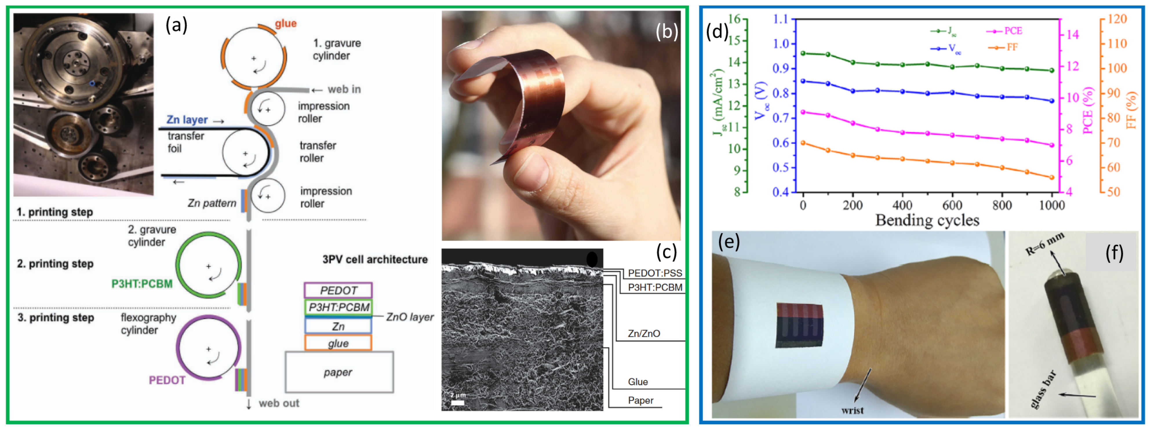
The first photovoltaic device fabricated on a paper substrate was a dye-sensitized cell reported by Wang and Kerr in 2011, using a nickel-coated paper as the conductive substrate supporting a ZnO photoanode sensitized with N719 dye [196]. Despite the modest efficiency of 1.21% (Voc = 0.56 V, Jsc = 6.70 mA/cm2, FF = 0.33), this demonstration established that paper-compatible low-temperature processing is viable (ZnO sintering at 90 °C rather than the 200 °C required for TiO2) as represented in Figure 11a–c. In the same year, Hübler et al. demonstrated the first solar cell on paper substrate free from ITO and Ag, using free patterning of all functional layers via printing and cold-foil transfer techniques, achieving 1.3% PCE on glossy printing paper (measured at 60 mW/cm2) [197].
Progress in OPV on cellulosic substrates accelerated significantly over the following decade. Zhou et al. in 2013 introduced cellulose nanocrystal (CNC) transparent films as substrates for OPV, achieving 2.7% PCE while simultaneously demonstrating room-temperature device disassembly and component recovery—the first solar cell for which a genuine end-of-life recycling route was shown experimentally [198]. Lin et al. in 2021 pushed further by developing free-standing TEMPO-oxidized cellulose nanofibril (TOCN) films embedding silver nanowire (AgNW) networks as ITO-free transparent electrodes, achieving a sheet resistance of 2.62 Ω/sq and 78.5% transmittance at 550 nm—performance comparable to PEN/ITO benchmarks—and demonstrating 7.47% PCE with stability over 500 bending cycles at a radius of 0.8 mm [199]. A step change occurred in 2024, when two independent groups demonstrated OPV efficiencies exceeding 18% on cellulose-derived substrates. Xiao et al. reported 18.05% PCE on an ethyl cellulose (EC)/polyimide hybrid film carrying an AgNW electrode (T = 88% at 550 nm, Rs = 17.65 Ω/sq), a result directly comparable to rigid ITO-glass references at that device generation [200]. Shortly thereafter, a world record for cellulose-substrate flexible OPV was established using an EC film crosslinked with an ETPTA polymer network, achieving 18.71% PCE with a specific power of 30.04 W·g−1 and mechanical stability at a bending radius of 1 mm over 10,000 cycles—a performance regime that conventional PET/ITO substrates cannot sustain at that radius (Figure 11d–f) [197].
For amorphous silicon, the most significant demonstration on paper remains the work of Smeets et al. ([184]), who applied UV nanoimprint lithography using an OrmoComp mould to transfer crater-like light-scattering textures onto Felix Schoeller FS-2 cellulose paper, simultaneously planarizing the fibrous surface and introducing efficient light trapping. The resulting a-Si:H cells achieved 5.5% PCE, directly comparable to the simultaneously processed textured glass reference at 5.6%. The NIL step is roll-to-roll compatible, and the authors noted its potential for upscaling to large-area and flexible device manufacturing [184]. By contrast, direct deposition of a-Si:H onto unplanarized photo paper without any surface engineering yielded only 1.08% PCE, underlining the critical role of roughness reduction in this device architecture [183].
Perovskite solar cells (PSCs) on paper have progressed from proof-of-concept to approaching competitive efficiencies, though the substrate class remains among the more challenging for this technology due to moisture sensitivity. Castro-Hermosa et al. demonstrated the first PSC on paper in 2017, without using adhesives, lamination or transfer processes, achieving 2.7% PCE through a stack of Au bottom electrode, SnO2, mesoporous TiO2, MAPbI3, Spiro-OMeTAD, and a MoOx/Au/MoOx semitransparent top contact with 62.5% transmittance and 9 Ω/sq sheet resistance [201]. Gao et al. in 2019 ([171]) advanced to nanocellulose paper coated with acrylic resin, reporting a transparent and biodegradable PSC substrate with PCE reaching 4.25% while the power per weight was 0.56 W g−1. The flexible PSCs also showed good stability, retaining >80% of original efficiency after 50 bending cycles. The relatively low FF of 34.65% reflects the limited sheet conductance of the ITO-free PEDOT:PSS anode, which the authors identified as the primary bottleneck for further efficiency gains [171]. An HTL-free architecture on cellulose paper was subsequently reported with 9.05% PCE (measured at 95 mW/cm2) and >75% retention after 1000 bending cycles, currently the highest PCE demonstrated for a PSC directly on a cellulosic paper substrate [202]. Notably, no higher PCE on paper has been reported since 2018, underscoring the persistent challenges that paper’s hygroscopicity and surface roughness pose for perovskite device integration.
Rounding out the paper substrate landscape, recently Synkiewicz-Musialska et al. compared regenerated cellulose (NatureFlex, certified compostable), gelatin-propylene glycol films, and PET as substrates for indoor OPV targeting IoT applications, using a soil-compatible carbon paste electrode throughout. The regenerated cellulose substrate achieved 15.88% PCE under LED at 1000 lx (indoor metric, not comparable to AM1.5G values), while the gelatin-based substrate failed during gravure printing due to thermal sensitivity [203].
Figure 11. Paper substrates. Fully printed SC. (a) Printing processes and respective layer architecture. (b) Photograph of the printed paper photovoltaic cell. (c) SEM image of the solar-cell cross-section [204]. Perovskite SC: (d) Plot of photovoltaic parameters as a function of bending cycles, (e) optical image of paper based HTM-free PSC attached on the wrist and (f) bent with R of 6 mm [202].
Solar 06 00028 g011
Textile Substrates
Three main fabrication strategies are commonly used for textile-based solar cells: direct layer-by-layer deposition onto the textile surface, stacking or transfer of prefabricated devices onto the fabric, and integration at the yarn intersection level. Each presents distinct trade-offs in terms of conformability, processing constraints, and device performance, as reviewed in detail by Ali et al. [168]. Here, we focus on selected representative examples within each technology class.
Plentz et al. ([176]), reported the first a-Si:H thin-film solar cell directly deposited on a woven textile, using Vitrulan glass fiber fabric dip-coated with a butadiene-styrene polymer to planarize the fiber surface. PECVD at 225 °C yielded Voc up to 883 mV, confirming shunt-free deposition on the non-planar substrate, with 1.4% PCE (FF 43.1%). The pseudo-FF of 70.2% from suns-Voc analysis identified the resistive 10 nm Ti semi-transparent contact as the primary bottleneck, with the authors projecting >5% PCE upon substitution with a transparent conductive oxide [176]. Plentz et al. ([175]), built on this foundation, replacing the dip-coat polymer with a PTFE coating that matched the thermal expansion coefficient of the glass fiber fabric more closely, enabling crack-free deposition. By integrating metal wires directly into the weave for electrical interconnection, they achieved 3.9% PCE (Voc = 876 mV, Jsc = 11.4 mA/cm2, FF = 39%, pseudo-FF = 79%), with the same diagnostic conclusion as before: series resistance at the contact, not the a-Si:H absorber quality, limits fill factor. A four-cell series-connected textile module reaching ~3 V was demonstrated as a proof of concept, as shown in Figure 12a [175].
Figure 12. Textile-based substrates. Amorphous silicon SC: (a) photo of solar cell array on glass fiber fabric with PTFE coating. (b) J–V curve and photovoltaic parameters of solar fabric with a-Si:H deposition at 180 °C [175]. OPV: (c) Plan view and (d) Cross-sectional view of woven 65/35 polyester cotton fabric substrate. (e) Interface coated fabric substrate. (f) Cross-sectional SEM image of spray coated functional layers’ sequence on the fabric substrate [189]. DSSC: (g) Schematic illustration (right column) and photographs (left column) of the process of inserting DSSCs into the textile during the weaving process with a six-heddle loom. (h) Current density–voltage (J–V) characteristics and power–voltage characteristics of representative inserted DSSCs in the textile. (i) Photograph of an inserted DSSC textile bent on the surface of a rod with a 1 cm radius of curvature [204]. Colored frames are used to group the panels according to the corresponding photovoltaic technology: amorphous silicon solar cells, OPV, and DSSC. Internal graphical elements, such as dots, arrows, and colored regions, are reproduced from the original cited sources.
Solar 06 00028 g012
For DSSC on textiles, Yun et al. ([204]) exemplified the third fabrication strategy identified above, integration at the yarn intersection level, by incorporating the cell electrodes directly during the weaving process: a dye-loaded TiO2-coated holed stainless-steel ribbon as photoanode and a Pt-loaded carbon yarn as counter-electrode were inserted as weft, with nylon warp threads serving as spacers to maintain electrode separation. This bypassed the friction and tension damage that had plagued earlier attempts to weave pre-fabricated PV wires, yielding 2.63% PCE (Voc = 0.725 V, Jsc = 5.78 mA/cm2, FF = 0.63) and stable performance down to 1 cm bending radius (Figure 12) [204]. Liu et al. ([185]) provided the clearest quantification of substrate roughness effects in textile DSSC. Using a screen-printed liquid-electrolyte architecture with a polyimide planarization layer, a 2.5-fold efficiency gap was measured between Kapton film (7.03%) and polyurethane-coated polyester-cotton fabric (2.78%), directly attributable to residual surface roughness after planarization [185]. A subsequent monolithic solid-state architecture deposited directly on glass fiber textile yielded only 0.4%, with the authors identifying roughness-induced shunting as the dominant loss mechanism [205]. No later work has substantially exceeded 2–3% on directly coated woven fabric substrates, underscoring that roughness management for textile DSSC remains an open problem. Fiber/yarn-type architectures, where TiO2 is grown or coated directly on individual metallic wires and two complementary wires are twisted together, have reached ~10% PCE on isolated wire cells, but this performance is not retained upon integration into actual woven structures, where mechanical forces during weaving damage the photovoltaic layers. The gap between wire-level and fabric-level efficiency thus remains the defining open challenge for textile DSSC, as reviewed in detail by Bandara et al. [172].
For OPV, Li et al. ([190]) demonstrated fully spray-coated OPV on 65/35 polyester-cotton fabric, using a screen-printed interface layer, applied in three passes to a total thickness of ~250 µm, as the essential planarization step before deposition of all functional layers [190]. Without this interface, earlier work from the same group had yielded only 0.02% PCE [206]; with it, 0.4% was achieved on fabric against 1.5% on an FTO glass reference. The encapsulated devices survived up to 90 days in air and 25 tensile bending cycles at 25 mm radius, establishing spray coating as a scalable, low-temperature route compatible with standard woven substrates. Jinno et al. ([193]) reported the washability benchmark for OPV on textiles via a transfer approach: ultrathin inverted cells (3 µm total, PNTz4T:PC71BM active layer, parylene substrate) were fabricated on glass, delaminated, and laminated onto textiles between two acrylic elastomer layers, achieving 7.9% PCE (Voc = 0.71 V, Jsc = 16.2 mA/cm2, FF = 68.9%) with only 5.4% efficiency loss after 120 min water immersion and 80% retention after 20 compression cycles with concurrent water exposure [193]. Since the textile serves solely as the final mechanical carrier rather than as a deposition substrate, this result speaks primarily to the wearability requirements discussed in Section 3.4.2 rather than to the substrate integration challenges addressed elsewhere in this section. The same group subsequently improved PCE to 10% via a thermally stable active layer integrated by hot-melt bonding [194] and further to 13.2% through non-fullerene acceptor engineering with doping-stabilized interfaces (Jiang et al., 2020 [207]), representing the current OPV efficiency ceiling for textile-integrated devices in this transfer configuration.
Jung et al. ([189]) provided the first demonstration of perovskite solar cells fabricated directly on a woven textile, using a polyester/satin substrate with a polyurethane planarization coating to suppress solvent infiltration and enable all-solution deposition of the full stack in an ITO-free architecture (PEDOT:PSS/CNT anode, MAPbI3 absorber, PCBM electron transport layer, thin Ag cathode). After solvent annealing of the 600 nm perovskite film, the best device achieved 5.72% PCE (Voc = 0.89 V, Jsc = 12.91 mA/cm2, FF = 0.51) on an active area of 6 mm2, with >80% retention after 300 h in ambient air without encapsulation [189]. Lam et al. ([195]) applied the same transfer logic as Jinno et al. ([192]), adhering a MAPbI3 device on ITO/PEN with electrodeposited SnO2/PCBM as the electron transport layer onto a textile via an acrylic elastomer encapsulant, achieving 14.3% PCE (Voc = 1.06 V, Jsc = 20.53 mA/cm2, FF = 0.66 at 1 sun) with >70% retention after 425 h in ambient air and resistance to 35 min water immersion. This remains the highest efficiency reported for a PSC in a textile-integrated configuration, with the same caveat that the textile serves solely as the final mechanical carrier rather than as a deposition substrate [195].
Yun et al. ([208]) set the upper efficiency bound for any PV technology on textile using a stress-assisted epitaxial lift-off (ELO) process: GaAs single-junction cells grown by MOCVD on a rigid wafer were transferred to woven fabric via an Au-Au bonding technique and a polyimide support layer, achieving 17.49% PCE. The practical constraints of this route (MOCVD cost, GaAs toxicity requiring full encapsulation, and the absence of washability testing) mean it represents an efficiency ceiling rather than a practical wearable technology [208].
Satharasinghe et al. ([192]) addressed all wearability requirements simultaneously through a different strategy: miniature c-Si cells encapsulated in resin micropods were soldered onto copper wire pairs and sheathed in knitted polyester to form solar E-yarns, which were then woven into fabric. The 44.5 × 45.5 mm2 demonstrator generated 2.15 mW/cm2 at 1 sun, retained ~90% output after 15 machine wash cycles, and preserved the breathability, drapeability, and moisture management of conventional textiles. It is the only textile PV result to satisfy all four wearability criteria simultaneously, at the cost of lower areal power density than thin-film approaches due to discrete cell spacing [192]. The performance data for both substrate families are collected in Table 12.
Table 12. Highlighted device results on paper and textile substrates.
TechnologySubstratePCE (%)YearKey Advance
Paper substrates
Fibrous cellulose paper
DSSC [209]Ni-coated paper1.212011First DSSC on paper; ZnO at 90 °C
OPV [204]Glossy printing paper1.3 a2011First fully printed, ITO-free and Ag-free OPV on paper; R2R process
PSC [201]Paper2.72017First PSC directly on paper; semitransparent top contact
a-Si:H [184]Cellulose paper (NIL textured, FS-2)5.52017UV nanoimprint planarization + light trapping; R2R compatible
a-Si:H [183]Photo paper (unplanarized)1.082018Roughness-penalty reference: no surface treatment
PSC [202]Cellulose paper, C electrode (HTL-free)9.05 b2018Highest PCE on paper; >75% retention after 1000 bending cycles
Cellulose-derived films c
OPV [198]CNC transparent film2.72013First recyclable solar cell; room-temperature disassembly demonstrated
PSC [171]Nanocellulose paper (NCP) + acrylic resin4.252019Transparent biodegradable PSC substrate; 0.56 W g−1
OPV [199]CNF/AgNW free-standing film7.472021ITO-free bio-based electrode; Rs = 2.62 Ω/sq; stable to 0.8 mm bending
OPV [200]Ethyl cellulose (EC) + AgNW18.052024First >18% OPV on a cellulose-derived substrate
OPV [197]EC@ETPTA crosslinked + AgNW18.712024World record OPV on cellulose; 30.04 W g−1; stable to 1 mm/10,000 cycles
OPV [203]Regenerated cellulose film (NatureFlex)15.88 d2025Certified compostable substrate; soil-compatible carbon paste electrode
Textile substrates
Direct deposition on textile
a-Si:H [176]Glass fiber textile (dip-coat polymer)1.42016First a-Si:H thin-film SC on woven textile; pseudo-FF 70.2%
a-Si:H [175]Glass fiber textile (PTFE coating)3.92025Best a-Si:H on textile; integrated wire interconnection; pseudo-FF 79%
DSSC [185]Polyester-cotton fabric (PU + PI layer)2.782018Roughness penalty quantified: 2.78% (fabric) vs. 7.03% (Kapton reference)
DSSC [205]Glass fiber textile (solid-state)0.42019Roughness-induced shunting identified as dominant loss mechanism
OPV [190]Polyester-cotton fabric (spray coating)0.42019Roughness threshold defined; all-spray route; 90-day encapsulated lifetime
PSC [189]Polyester/satin (PU coating)5.722018First PSC directly on woven textile; ITO-free; >80% retention at 300 h
Yarn-level integration (weaving-in)
DSSC [210]Woven structure (nylon warp spacers)2.632015First DSSC integrated during weaving; stable to 1 cm bending radius
Transfer/stacking onto textile
OPV [193]Parylene substrate → elastomer → textile7.92017Washability benchmark; 5.4% loss after 120 min water immersion
OPV [194]Parylene substrate → hot-melt → textile102018Thermal stability to 120 °C; no performance loss on textile integration
OPV [207]Parylene substrate → textile13.22020OPV efficiency ceiling for transfer configuration; T80 > 11 years
PSC [195]ITO/PEN → elastomer → textile14.32017Highest PCE for PSC on textile; >70% retention at 425 h; waterproof
GaAs [208] MOCVD wafer → ELO transfer to fabric17.492022Highest PCE on textile (any technology); efficiency ceiling demonstration
a Measured at 60 mW/cm2 (not AM1.5G standard); efficiency not directly comparable to other entries. b Measured at 95 mW/cm2; not directly comparable to AM1.5G values. c Cellulose-derived films (CNC, CNF, ethyl cellulose, regenerated cellulose) differ fundamentally from fibrous paper in surface morphology and are included here for their bio-based character; they are physically closer to polymer substrates than to conventional paper. d Indoor metric only: LED illumination at 1000 lx; not comparable to AM1.5G values.

4. Integrated Substrate Landscape

4.1. Integration Constraints of Non-Conventional Substrates

Despite their differences in composition and microstructure the impact of the different substrates on device performance is, in many cases, determined by a set of common physical phenomena. Table 13 summarizes these constraints for the main substrate families discussed in this review, aiming to link the intrinsic properties of each substrate with the main challenges they present for the integration of photovoltaic solar systems. This indicates that the complexity associated with non-conventional substrates does not come from some particular defects, but from the interaction between their surface properties, internal microstructure, and the requirements of the device to be deposited.
From this perspective, each substrate family presents a specific combination of constraints that determines how and what type of photovoltaic devices can be integrated. Ceramic substrates concentrate challenges related to micrometric roughness and alkali migration; metallic substrates to transition metal diffusion and electrical boundary conditions; polymeric substrates to limited thermal processing and high permeability; and porous systems to multi-species transport and structural heterogeneity. However, the underlying physical framework is common.
Rather than focusing on the type of material, this approach allows the dominant physical constraints to be identified first. Based on these, both substrate selection and device architecture can be defined.

4.2. Advantanges and Opportunities of Non-Conventional Substrates

Although the previous section discusses their main limitations, non-conventional substrates also provide important opportunities. Their adoption opens the door to the incorporation of photovoltaic solar systems into application scenarios that cannot be achieved with traditional platforms.
Glass continues to offer a highly optimized combination of flatness, chemical stability, low permeability, and industrial maturity. For this reason, it remains the reference substrate for large-area rigid photovoltaic modules. However, its rigidity, weight, and limited structural integration capacity restrict its use across a wide range of applications.
Ceramic substrates, particularly glazed tiles, enable direct structural integration across the entire building while simultaneously forming part of the construction element itself. Their thermal stability, exceeding 1000 °C in many cases, together with their high mechanical robustness, makes them compatible with absorbers requiring high-temperature treatments, while also offering aesthetic integration possibilities in BIPV applications.
Metallic substrates, in contrast, are good candidates for structurally demanding environments such as aerospace applications, mobile systems, or flexible devices. In certain cases, metallic foils can also simplify device architecture by acting as conductive back contacts, provided that diffusion and electrical insulation phenomena are properly controlled.
Polymeric substrates enable lightweight, conformable photovoltaic devices manufactured through continuous and scalable processes such as roll-to-roll. Their flexibility allows it integration on curved surfaces, portable devices, or wearable systems, scenarios that are not accessible with rigid substrates, thereby defining a specific space for low-temperature photovoltaic technologies with high mechanical conformability.
Porous and fibrous substrates further expand the possibilities toward integration into textiles and multifunctional materials. Their high surface area and structural versatility make it possible to conceive hybrid systems in which energy generation can be combined with additional functions, such as structural reinforcement or textile integration.
In this context, non-conventional substrates should not be evaluated only in terms of integration difficulty, but in terms of the functional domain they enable. There is no universally optimal substrate, each family defines a specific trade-off between stability, mechanical behavior, processing window, and application environment.

4.3. Comparative Performance, Economic Viability and Substrate Selection

To complement the substrate-specific discussion, Table 14 provides a cross-technology comparison of the highest efficiencies reported in this review for representative photovoltaic technologies on non-conventional substrates. These values are compared with current record or reference efficiencies for the corresponding technologies on conventional or optimized substrates. The comparison should not be interpreted as a direct measurement of substrate-induced loss in all cases, since the reported devices often differ in absorber composition, device architecture, active area, processing route and measurement conditions. Nevertheless, it provides a useful indication of the technological maturity of each substrate–technology combination.
In addition to photovoltaic performance, Table 14 also summarizes the main substrate-related limitations, recommended application domains and qualitative economic considerations for each substrate family. This qualitative assessment highlights that economic viability is not determined only by the intrinsic cost of the substrate, but also by surface preparation, planarization, barrier layers, encapsulation, process scalability, expected lifetime and the added value of the final application.
Based on the constraints discussed above, substrate selection can be approached as a sequential decision process rather than as a direct comparison of material families. Figure 13 provides a practical flowchart linking the main application requirements with compatible substrate classes. The first selection criterion is usually the thermal budget imposed by the photovoltaic technology, followed by mechanical flexibility, electrical conductivity, surface roughness/permeability and manufacturing scale. This approach highlights that the most economically efficient substrate is not necessarily the cheapest material, but the one that minimizes the total integration penalty, including planarization, barrier layers, encapsulation, processing yield and application-specific lifetime.

Outlook and Open Questions

Overall, the most promising substrate–technology combinations are those in which the processing requirements of the photovoltaic stack are naturally aligned with the intrinsic properties of the substrate. Ceramic and building-derived substrates are particularly attractive for BIPV-oriented thin-film technologies, such as CIGS, CIS, Sb2Se3 and a-Si:H, provided that glaze roughness, porosity and alkali diffusion are controlled. Metallic substrates remain among the most mature options for high-performance flexible thin-film photovoltaics, especially CIGS-based devices, although stable operation requires effective electrical insulation and diffusion-barrier layers. Polymeric substrates are best suited to lightweight, flexible and roll-to-roll-compatible devices based on low-temperature technologies such as OPV and PSCs, while paper-, cellulose- and textile-based substrates are most promising for indoor photovoltaics, sustainable electronics, wearables and low-power applications.
Conversely, some combinations remain strongly constrained. Direct deposition of high-temperature absorbers on untreated paper, natural textiles or thermally unstable polymers is generally limited by thermal degradation, outgassing, dimensional instability and poor surface planarity. Similarly, direct fabrication of ultrathin OPV or PSC stacks on rough woven textiles remains challenging because of multiscale roughness, pinhole formation and shunting. Key open questions therefore include the control of substrate-induced diffusion at grain boundaries and local defects, the establishment of quantitative roughness–shunting relationships, the development of scalable barrier and planarization layers, and the assessment of long-term reliability under coupled thermal, humidity, mechanical and application-specific stresses.

5. Conclusions

This work analyses the integration of photovoltaic devices on non-conventional substrates from a unified physical perspective. Although ceramic, metallic, polymeric, and porous substrates differ significantly in composition and application context, their impact on device performance can be largely understood through the phenomena described above, which enables a more systematic view of integration limits.
At the same time, non-conventional substrates should not only be evaluated in terms of technological complexity. Each family of materials has a specific optimal application field: structural integration in the case of ceramics, mechanical resilience and lightweight architectures for metallic substrates, conformability and low-cost manufacturing for polymers and textile or multifunctional integration for porous materials. These substrates do not necessarily compete with one another; rather, they expand the application space of photovoltaic technologies. Each case represents a specific balance between stability, processability, mechanical behavior and application environment. The future of photovoltaic integration will not only be determined by absorber efficiency, but by the intelligent alignment between substrate properties, device architecture, and application environment. Understanding and engineering these factors will be key to the development of the next generation of integrated photovoltaic systems.

Author Contributions

Conceptualization, S.P.-G., D.M.-R. and J.B.C.; resources, D.M.-R. and J.B.C.; writing—original draft preparation, S.P.-G., A.L., S.T., D.T.P. and J.G.C.; writing—review and editing, all authors; supervision, D.M.-R. and J.B.C.; project administration, D.M.-R. and J.B.C.; funding acquisition, D.M.-R. and J.B.C. All authors have read and agreed to the published version of the manuscript.

Funding

This research was funded by the CLUSKER project (INNEST/2024/420), funded by the Valencian Institute of Business Competitiveness (IVACE), and by the REACTIVE project (ANR-21-CE08-0047), funded by the Agence Nationale de la Recherche (ANR). This work was also supported by the postdoctoral contract CIAPOS/2023/425 and the predoctoral contract CIACIF/2022/277, both cofunded by the Valencian Community Government and the European Social Fund. Additional financial support was provided by the “Cátedra de Innovación Cerámica ‘Ciutat de Vila-real’ de l’Universitat Jaume I”. The APC was waived by the journal.

Data Availability Statement

No new data were created or analyzed in this study. Data sharing is not applicable to this article.

Acknowledgments

The authors would like to thank their respective institutions and research groups for their support during the preparation of this manuscript.

Conflicts of Interest

The authors declare no conflicts of interest.

Abbreviations

The following abbreviations are used in this manuscript:
AFMAtomic force microscopy
AgNWSilver nanowire
ALDAtomic layer deposition
AM1.5GAir mass 1.5 global solar spectrum
AZOAluminum-doped zinc oxide
BCPBathocuproine
BIPVBuilding-integrated photovoltaics
CBDChemical bath deposition
CdTeCadmium telluride
CIGSCopper indium gallium selenide
CISCopper indium selenide
CNCCellulose nanocrystal
CNFCellulose nanofibril
CNTCarbon nanotube
CPIColorless polyimide
CTECoefficient of thermal expansion
CVDChemical vapor deposition
CZTSCopper zinc tin sulfide
CZTSSeCopper zinc tin sulfide/selenide
DSSCDye-sensitized solar cell
ECEthyl cellulose
EDXEnergy-dispersive X-ray spectroscopy
ELOEpitaxial lift-off
ETPTAEthoxylated trimethylolpropane triacrylate
FFFill factor
FS-2Felix Schoeller FS-2 cellulose paper
FTOFluorine-doped tin oxide
HiPIMSHigh-power impulse magnetron sputtering
HTLHole transport layer
HTMHole transport material
IBADIon-beam-assisted deposition
ITOIndium tin oxide
IoTInternet of Things
J–VCurrent density–voltage
JscShort-circuit current density
LEDLight-emitting diode
MOCVDMetal-organic chemical vapor deposition
NCPNanocellulose paper
NILNanoimprint lithography
OPVOrganic photovoltaics
OSCOrganic solar cell
PCBMPhenyl-C61-butyric acid methyl ester
PCEPower conversion efficiency
PDMSPolydimethylsiloxane
PECVDPlasma-enhanced chemical vapor deposition
PEDOT:PSSPoly(3,4-ethylenedioxythiophene):poly(styrenesulfonate)
PENPolyethylene naphthalate
PETPolyethylene terephthalate
PIPolyimide
PSCPerovskite solar cell
PTFEPolytetrafluoroethylene
PUPolyurethane
PVPhotovoltaic
PVDPhysical vapor deposition
R2RRoll-to-roll
RaArithmetic average roughness
RqRoot mean

References

  1. Al-Ali, S.; Olabi, A.G.; Mahmoud, M. A Review of Solar Photovoltaic Technologies: Developments, Challenges, and Future Perspectives. Energy Convers. Manag. X 2025, 27, 101057. [Google Scholar] [CrossRef] [Scilit]
  2. Singh, B.P.; Goyal, S.K.; Kumar, P. Solar PV Cell Materials and Technologies: Analyzing the Recent Developments. Mater. Today Proc. 2021, 43, 2843–2849. [Google Scholar] [CrossRef] [Scilit]
  3. Bórawski, P.; Holden, L.; Bełdycka-Bórawska, A. Perspectives of Photovoltaic Energy Market Development in the European Union. Energy 2023, 270, 126804. [Google Scholar] [CrossRef] [Scilit]
  4. Li, X.; Li, P.; Wu, Z.; Luo, D.; Yu, H.-Y.; Lu, Z.-H. Review and Perspective of Materials for Flexible Solar Cells. Mater. Rep. Energy 2021, 1, 100001. [Google Scholar] [CrossRef] [Scilit]
  5. Goldschmidt, J.C.; Wagner, L.; Pietzcker, R.; Friedrich, L. Technological Learning for Resource Efficient Terawatt Scale Photovoltaics. Energy Environ. Sci. 2021, 14, 5147–5160. [Google Scholar] [CrossRef] [Scilit]
  6. Piliougine, M.; Garcia-Marrero, L.E.; Lappalainen, K.; Spagnuolo, G. Influence of the Temperature on the Intrinsic Parameters of Thin-Film Photovoltaic Modules. Renew. Energy 2025, 240, 122068. [Google Scholar] [CrossRef] [Scilit]
  7. Priya, P.; Stonier, A.A. Emerging Innovations in Solar Photovoltaic (PV) Technologies: The Perovskite Solar Cells and More. Energy Rep. 2025, 14, 216–242. [Google Scholar] [CrossRef] [Scilit]
  8. Piliougine, M.; Sánchez-Friera, P.; Petrone, G.; Sánchez-Pacheco, F.J.; Spagnuolo, G.; Sidrach-de-Cardona, M. New Model to Study the Outdoor Degradation of Thin–Film Photovoltaic Modules. Renew. Energy 2022, 193, 857–869. [Google Scholar] [CrossRef] [Scilit]
  9. Meddeb, H.; Götz-Köhler, M.; Neugebohrn, N.; Banik, U.; Osterthun, N.; Sergeev, O.; Berends, D.; Lattyak, C.; Gehrke, K.; Vehse, M. Tunable Photovoltaics: Adapting Solar Cell Technologies to Versatile Applications. Adv. Energy Mater. 2022, 12, 2200713. [Google Scholar] [CrossRef] [Scilit]
  10. Ali, A.O.; Elgohr, A.T.; El-Mahdy, M.H.; Zohir, H.M.; Emam, A.Z.; Mostafa, M.G.; Al-Razgan, M.; Kasem, H.M.; Elhadidy, M.S. Advancements in Photovoltaic Technology: A Comprehensive Review of Recent Advances and Future Prospects. Energy Convers. Manag. X 2025, 26, 100952. [Google Scholar] [CrossRef] [Scilit]
  11. Li, J.; Xie, H.; Zhang, J.; Li, L.; Song, G.; Fu, H.; Chen, P.; Liu, C.; Zhang, L.; Shi, Z.; et al. A Systematic Review of Reinforcement Learning in Building-Integrated Photovoltaic (BIPV) Optimization. Adv. Appl. Energy 2025, 19, 100239. [Google Scholar] [CrossRef] [Scilit]
  12. Zhou, N.; Wang, N.; Wang, H.; Xie, H.; Zhang, Y.; Ao, H. Optical 3d µ-Printing of Pvdf-Based Flexible Microstructural Auxetic Metamaterials and 3d Microgrid Pyramid Arrays for Wearable Electronics. Chem. Eng. J. 2025, 516, 163956. [Google Scholar] [CrossRef] [Scilit]
  13. Jeong, H.-S.; Ki, T.; Lim, D.; Lee, S.; Jang, J.-H.; Kim, S.; Lee, K.; Kang, H. Realizing the Potential of Scalable and Stable Semitransparent Organic Solar Modules. Chem. Eng. J. 2025, 503, 158497. [Google Scholar] [CrossRef] [Scilit]
  14. Wu, Y.; Huang, H.; Cao, Y.; Wang, B.; Li, X.; Song, X.; Pang, Z.; Jiang, T.; Lu, Y.; Tan, G. Photovoltaic Material Selection and Multi-Objective Building Design Optimization for Enhancing Energy Performance of Building Integrated Photovoltaics (BIPV) Systems. Appl. Energy 2026, 406, 127270. [Google Scholar] [CrossRef] [Scilit]
  15. Delgado-Sanchez, J.M.; Larrañeta, M.; Lillo-Bravo, I. Functional and Semi-Transparent CIS Solar Cells Deposited on Aesthetic Ceramic Substrates for Building Integrated Photovoltaic Applications. Appl. Surf. Sci. 2026, 724, 165742. [Google Scholar] [CrossRef] [Scilit]
  16. Casariego, P.; Sarrablo, V.; Barrientos, R.; Ibraikulov, O.A.; Cros, S. Second Photovoltaic Prototype for Textile Ceramic Technology: The Perovskite Glass Solar Brick. Constr. Build. Mater. 2025, 493, 143143. [Google Scholar] [CrossRef] [Scilit]
  17. Kwaśnicki, P. Texturized Glass in the Application of Architectural Photovoltaics. Clean. Eng. Technol. 2024, 22, 100810. [Google Scholar] [CrossRef] [Scilit]
  18. Batista, F.; Guimarães, A.S.; Palmero-Marrero, A.I. Building Integrated Photovoltaics: A Multi-Level Design Review for Optimized Implementation. Renew. Sustain. Energy Rev. 2025, 220, 115837. [Google Scholar] [CrossRef] [Scilit]
  19. Park, H.K.; Jo, W. Flexible Cu(In,Ga)Se2 Photovoltaics for Bending Applications: Advances from Materials to Panels. J. Mater. Chem. C 2025, 13, 2554–2577. [Google Scholar] [CrossRef] [Scilit]
  20. Li, L.; Han, L.; Hu, H.; Zhang, R. A Review on Polymers and Their Composites for Flexible Electronics. Mater. Adv. 2023, 4, 726–746. [Google Scholar] [CrossRef] [Scilit]
  21. Zhang, P.; Yang, H.; Zheng, Q.; Nie, G.; Abdullah Alzahrani, A.Y.; Al-Buriahi, M.S.; Alsaiari, N.S.; Raza, S.; Orooji, Y. Next-Generation Solar Energy: Progress, Stability, and Prospects of Polymer-Modified Perovskite Solar Cells; A Review. Int. J. Hydrogen Energy 2025, 106, 1088–1113. [Google Scholar] [CrossRef] [Scilit]
  22. Intal, D.; Ebong, A. Thin-Film Solar Photovoltaics: Trends and Future Directions. In Proceedings of the 2024 IEEE 21st International Conference on Smart Communities: Improving Quality of Life Using AI, Robotics and IoT (HONET); IEEE: Doha, Qatar, 2024; pp. 135–142. [Google Scholar]
  23. Cosme, I.; Carrillo-Sendejas, J.C.; Guerra-Hernandez, S.F.; Sánchez Vergara, M.E.; Carlos, N.; Moreno, M. Xanthan Gum as a Green, Non-Toxic, Surfactant-Free Modifier for Enhanced Deposition of PEDOT: PSS in Crystalline Silicon Hybrid Solar Cells. Surf. Interfaces 2025, 72, 107232. [Google Scholar] [CrossRef] [Scilit]
  24. Nuayi, A.W.; Ruslan, R.; Irzaman; Winata, T.; Noor, F.A. Scalable Low-Temperature Growth of Graphene Window Layers Using HW IP–VHF–PECVD for Efficient Silicon Solar Cells: The Influence of Different Chamber Pressures on Optoelectrical Performance. Mater. Sci. Eng. B 2026, 324, 118969. [Google Scholar] [CrossRef] [Scilit]
  25. Nisa, Q.A.K.; Nasrun, R.F.B.; Son, D.H.; Kim, J.H. Unraveling Charge Transport and Stability Mechanism in Non-Halogenated Phenothiazine Self-Assembled Monolayer for 19.7% High Performance Organic Solar Cell. Mater. Today Energy 2026, 56, 102195. [Google Scholar] [CrossRef] [Scilit]
  26. Adhikari, T.; Shahiduzzaman, M.; Yamamoto, K.; Lebel, O.; Nunzi, J.-M. Interfacial Modification of the Electron Collecting Layer of Low-Temperature Solution-Processed Organometallic Halide Photovoltaic Cells Using an Amorphous Perylenediimide. Sol. Energy Mater. Sol. Cells 2017, 160, 294–300. [Google Scholar] [CrossRef] [Scilit]
  27. Polman, A.; Knight, M.; Garnett, E.C.; Ehrler, B.; Sinke, W.C. Photovoltaic Materials: Present Efficiencies and Future Challenges. Science 2016, 352, aad4424. [Google Scholar] [CrossRef] [Scilit]
  28. Majhi, J.; Ghosh, S.; Priya, K.; Sharma, S.; Bandyopadhyay, A. A Critical Review on the Progress of Emerging Active and Substrate Materials for Organic Solar Cells and Device Level Fabrication Techniques by Solution Process Method. Next Mater. 2025, 8, 100595. [Google Scholar] [CrossRef] [Scilit]
  29. Mathew, X.; Enriquez, J.P.; Romeo, A.; Tiwari, A.N. CdTe/CdS Solar Cells on Flexible Substrates. Sol. Energy 2004, 77, 831–838. [Google Scholar] [CrossRef] [Scilit]
  30. Pimpinelli, A.; Villain, J. Physics of Crystal Growth; Collection Alea-Saclay: Monographs and Texts in Statistical Physics; Cambridge University Press: Cambridge, UK, 1998. [Google Scholar]
  31. Venables, J.A.; Spiller, G.D.T.; Hanbucken, M. Nucleation and Growth of Thin Films. Rep. Prog. Phys. 1984, 47, 399. [Google Scholar] [CrossRef] [Scilit]
  32. Schorr, S. The Crystal Structure of Kesterite Type Compounds: A Neutron and X-Ray Diffraction Study. Sol. Energy Mater. Sol. Cells 2011, 95, 1482–1488. [Google Scholar] [CrossRef] [Scilit]
  33. Roland, S.; Hans-Werner, S. Chalcogenide Photovoltaics Physics, Technologies, and Thin Film Devices; WILEY-VCH: Weinheim, Germany, 2011. [Google Scholar]
  34. Marino, C.E.B.; Nascente, P.A.P.; Biaggio, S.R.; Rocha-Filho, R.C.; Bocchi, N. XPS Characterization of Anodic Titanium Oxide Films Grown in Phosphate Buffer Solutions. Thin Solid Film. 2004, 468, 109–112. [Google Scholar] [CrossRef] [Scilit]
  35. Sangale, S.S.; Mann, D.S.; Lee, H.-J.; Kwon, S.-N.; Na, S.-I. Influence of Interfacial Roughness on Slot-Die Coatings for Scaling-up High-Performance Perovskite Solar Cells. Commun. Mater. 2024, 5, 201. [Google Scholar] [CrossRef] [Scilit]
  36. Feleki, B.T.; Bouwer, R.K.M.; Wienk, M.M.; Janssen, R.A.J. Perovskite Solar Cells on Polymer-Coated Smooth and Rough Steel Substrates. Sol. RRL 2022, 6, 2100898. [Google Scholar] [CrossRef] [Scilit]
  37. Jehl, Z.; Bouttemy, M.; Lincot, D.; Guillemoles, J.F.; Gerard, I.; Etcheberry, A.; Voorwinden, G.; Powalla, M.; Naghavi, N. Insights on the Influence of Surface Roughness on Photovoltaic Properties of State of the Art Copper Indium Gallium Diselenide Thin Films Solar Cells. J. Appl. Phys. 2012, 111, 114509. [Google Scholar] [CrossRef] [Scilit]
  38. Yang, G.; Yu, Z.J.; Wang, M.; Shi, Z.; Ni, Z.; Jiao, H.; Fei, C.; Wood, A.; Alasfour, A.; Chen, B.; et al. Shunt Mitigation toward Efficient Large-Area Perovskite-Silicon Tandem Solar Cells. Cell Rep. Phys. Sci. 2023, 4, 101628. [Google Scholar] [CrossRef] [Scilit]
  39. Maurya, S.; Labeyrie, L.; Zimny, K.; Rodriguez-Robles, M.D.M.; Zheng, B.; Schumacher, S.; Muñoz-Rojas, D.; Bellet, D.; Tréguer-Delapierre, M. Recent Advances in Metallic Nanowire Based Transparent Electrodes: From Chemistry of Metallic Nanowires to Physics behind the Conducting Networks. Adv. Phys. X 2025, 10, 2573818. [Google Scholar] [CrossRef] [Scilit]
  40. Piperno, L.; Celentano, G. Solution Deposition Planarization as an Alternative to Electro-Mechanical Polishing for HTS Coated-Conducters. Coatings 2025, 15, 45. [Google Scholar] [CrossRef] [Scilit]
  41. Sato, D.; Kobayashi, H.; Masuda, T.; Araki, K.; Miyashita, Y.; Yamada, N. Structural Design and Demonstration of Three-Dimensional Curved Photovoltaic Modules Using Crystalline Silicon Solar Cells. Sol. Energy Mater. Sol. Cells 2025, 279, 113258. [Google Scholar] [CrossRef] [Scilit]
  42. Thornber, T.; Game, O.S.; Cassella, E.J.; O’Kane, M.E.; Bishop, J.E.; Routledge, T.J.; Alanazi, T.I.; Togay, M.; Isherwood, P.J.M.; Infante-Ortega, L.C.; et al. Nonplanar Spray-Coated Perovskite Solar Cells. ACS Appl. Mater. Interfaces 2022, 14, 37587–37594. [Google Scholar] [CrossRef] [Scilit]
  43. Howden, R.M.; Flores, E.J.; Bulović, V.; Gleason, K.K. The Application of Oxidative Chemical Vapor Deposited (oCVD) PEDOT to Textured and Non-Planar Photovoltaic Device Geometries for Enhanced Light Trapping. Org. Electron. 2013, 14, 2257–2268. [Google Scholar] [CrossRef] [Scilit]
  44. Brooks, D.J.; Merinov, B.V.; Goddard, W.A.; Kozinsky, B.; Mailoa, J. Atomistic Description of Ionic Diffusion in PEO–LiTFSI: Effect of Temperature, Molecular Weight, and Ionic Concentration. Macromolecules 2018, 51, 8987–8995. [Google Scholar] [CrossRef] [Scilit]
  45. Haruyama, J.; Sodeyama, K.; Han, L.; Tateyama, Y. First-Principles Study of Ion Diffusion in Perovskite Solar Cell Sensitizers. J. Am. Chem. Soc. 2015, 137, 10048–10051. [Google Scholar] [CrossRef] [Scilit]
  46. Calvet, I.; Barrachina, E.; Martí, R.; Fraga, D.; Stoyanova Lyubenova, T.; Carda, J.B. Development of Photovoltaic Ceramic Tile Based on CZTSSe Absorber. Mater. Lett. 2015, 161, 636–639. [Google Scholar] [CrossRef] [Scilit]
  47. Fraga, D.; Stoyanova Lyubenova, T.; Martí, R.; Calvet, I.; Barrachina, E.; Carda, J.B. Ecologic Ceramic Substrates for CIGS Solar Cells. Ceram. Int. 2016, 42, 7148–7154. [Google Scholar] [CrossRef] [Scilit]
  48. Eames, C.; Frost, J.M.; Barnes, P.R.F.; O’Regan, B.C.; Walsh, A.; Islam, M.S. Ionic Transport in Hybrid Lead Iodide Perovskite Solar Cells. Nat. Commun. 2015, 6, 7497. [Google Scholar] [CrossRef] [Scilit] [PubMed]
  49. Greenbank, W. Interfacial Stability and Degradation in Organic Photovoltaic Solar Cells. Available online: https://theses.hal.science/tel-01552294v2 (accessed on 15 February 2026).
  50. Tong, H.; Wu, X.; Wang, X.; Xu, X.; Guo, M.; Liao, B.; Ma, S.; Li, Z.; Hoex, B. Mitigating Contaminant-Induced Surface Degradation in TOPCon Solar Cells: Mechanisms, Impacts, and Mitigation. Sol. Energy Mater. Sol. Cells 2025, 286, 113558. [Google Scholar] [CrossRef] [Scilit]
  51. Penukula, S.; Khanal, M.N.; Sharma, M.; Parashar, M.; Kerner, R.A.; Chen, M.; Davis, M.A.; Saha, R.A.; Solano, E.; Roeffaers, M.B.J.; et al. Barrier Layer Design Reduces Top Electrode Ion Migration in Perovskite Solar Cells. EES Sol. 2025, 1, 345–355. [Google Scholar] [CrossRef] [Scilit]
  52. Zhang, S.; Liu, Z.; Zhang, W.; Jiang, Z.; Chen, W.; Chen, R.; Huang, Y.; Yang, Z.; Zhang, Y.; Han, L.; et al. Barrier Designs in Perovskite Solar Cells for Long-Term Stability. Adv. Energy Mater. 2020, 10, 2001610. [Google Scholar] [CrossRef] [Scilit]
  53. Schlesinger, M.; Paunovic, M.; Electrochemical Society (Eds.) Modern Electroplating, 5th ed.; Electrochemical Society Series; John Wiley & Sons, Inc.: Hoboken, NJ, USA, 2010. [Google Scholar]
  54. National Research Council (U.S.); Panel on Review and Evaluation of Alternative Chemical Disposal Technologies; Board on Army Science and Technology. Review and Evaluation of Alternative Chemical Disposal Technologies, 1st ed.; Alternative Chemical Disposal Technologies; National Academy Press: Washington, DC, USA, 1996.
  55. George, S.M. Atomic Layer Deposition: An Overview. Chem. Rev. 2010, 110, 111–131. [Google Scholar] [CrossRef] [Scilit]
  56. Hoye, R.L.Z.; Muñoz-Rojas, D.; Sun, Z.; Okcu, H.; Asgarimoghaddam, H.; MacManus-Driscoll, J.L.; Musselman, K.P. Spatial Atomic Layer Deposition for Energy and Electronic Devices. PRX Energy 2025, 4, 17002. [Google Scholar] [CrossRef] [Scilit]
  57. Hunter, R.J. (Ed.) Chapter 2—Charge and Potential Distribution at Interfaces. In Zeta Potential in Colloid Science; Academic Press: Cambridge, MA, USA, 1981; pp. 11–58. [Google Scholar]
  58. Hunter, R.J. (Ed.) Chapter 3—The Calculation of Zeta Potential. In Zeta Potential in Colloid Science; Academic Press: Cambridge, MA, USA, 1981; pp. 59–124. [Google Scholar]
  59. Thornton, J.A. Influence of Apparatus Geometry and Deposition Conditions on the Structure and Topography of Thick Sputtered Coatings. J. Vac. Sci. Technol. 1974, 11, 666–670. [Google Scholar] [CrossRef] [Scilit]
  60. Greene, J.E. Review Article: Tracing the Recorded History of Thin-Film Sputter Deposition: From the 1800s to 2017. J. Vac. Sci. Technol. A Vac. Surf. Film. 2017, 35, 5C204. [Google Scholar] [CrossRef] [Scilit]
  61. Houzibe, R.; El-Kettani, M.E.-C.; Maréchal, P.; Siryabe, E.; Betchewe, G. Discrimination between Weak Adhesion, Delamination and Kissing Bond at the Interfaces of Composite Bonded Assemblies. Wave Motion 2023, 118, 103105. [Google Scholar] [CrossRef] [Scilit]
  62. Khanna, V.K. Adhesion–Delamination Phenomena at the Surfaces and Interfaces in Microelectronics and MEMS Structures and Packaged Devices. J. Phys. D Appl. Phys. 2011, 44, 34004. [Google Scholar] [CrossRef] [Scilit]
  63. Jaegermann, W.; Klein, A.; Mayer, T. Interface Engineering of Inorganic Thin-Film Solar Cells—Materials-Science Challenges for Advanced Physical Concepts. Adv. Mater. 2009, 21, 4196–4206. [Google Scholar] [CrossRef] [Scilit]
  64. Chandrasekaran, R.; Itskov, M.; Rege, A. Influence of Microstructure on the Mechanical Behavior of Open-Porous Materials under Large Strains. Int. J. Solids Struct. 2025, 319, 113441. [Google Scholar] [CrossRef] [Scilit]
  65. Liu, H.; Zhao, X. Thermal Conductivity Analysis of High Porosity Structures with Open and Closed Pores. Int. J. Heat Mass Transf. 2022, 183, 122089. [Google Scholar] [CrossRef] [Scilit]
  66. Ortiz-Marqués, A.; Caldevilla, P.; Goldmann, E.; Safuta, M.; Fernández-Raga, M.; Górski, M. Porosity and Permeability in Construction Materials as Key Parameters for Their Durability and Performance: A Review. Buildings 2025, 15, 3422. [Google Scholar] [CrossRef] [Scilit]
  67. Robeson, L.M. Correlation of Separation Factor versus Permeability for Polymeric Membranes. J. Membr. Sci. 1991, 62, 165–185. [Google Scholar] [CrossRef] [Scilit]
  68. Norton, F.J. Permeation of Gases through Solids. J. Appl. Phys. 1957, 28, 34–39. [Google Scholar] [CrossRef] [Scilit]
  69. Yao, J.; Iqbal, A.; Juneja, H.; Shadman, F. Moisture Uptake and Outgassing in Patterned and Capped Porous Low-k Dielectric Films. J. Electrochem. Soc. 2007, 154, G199. [Google Scholar] [CrossRef] [Scilit]
  70. Figini-Albisetti, A.; Velasco, L.F.; Parra, J.B.; Ania, C.O. Effect of Outgassing Temperature on the Performance of Porous Materials. Appl. Surf. Sci. 2010, 256, 5182–5186. [Google Scholar] [CrossRef] [Scilit]
  71. Gundlach, B.; Blum, J. Outgassing of Icy Bodies in the Solar System—II: Heat Transport in Dry, Porous Surface Dust Layers. Icarus 2012, 219, 618–629. [Google Scholar] [CrossRef] [Scilit]
  72. Jordan, D.C.; Kurtz, S.R. Photovoltaic Degradation Rates—An Analytical Review. Prog. Photovolt. 2013, 21, 12–29. [Google Scholar] [CrossRef] [Scilit]
  73. Alstrup, J.; Norrman, K.; Jørgensen, M.; Krebs, F.C. Lifetimes of Organic Photovoltaics: Design and Synthesis of Single Oligomer Molecules in Order to Study Chemical Degradation Mechanisms. Sol. Energy Mater. Sol. Cells 2006, 90, 2777–2792. [Google Scholar] [CrossRef] [Scilit]
  74. Kaviany, M. Principles of Heat Transfer in Porous Media; Mechanical Engineering Series; Springer: New York, NY, USA, 1995. [Google Scholar]
  75. Ohring, M. (Ed.) Chapter 12—Mechanical Properties of Thin Films. In Materials Science of Thin Films, 2nd ed.; Academic Press: San Diego, CA, USA, 2002; pp. 711–781. [Google Scholar]
  76. Papargyri, L.; Papanastasiou, P.; Georghiou, G.E. Sequential Thermomechanical Stress and Cracking Analysis of Photovoltaic Modules with Full and Half-Cut Cells. Sol. Energy Mater. Sol. Cells 2024, 278, 113166. [Google Scholar] [CrossRef] [Scilit]
  77. Erdil, U.; Khenkin, M.; Bernardes De Araujo, W.M.; Emery, Q.; Lauermann, I.; Paraskeva, V.; Norton, M.; Vediappan, S.; Kumar, D.K.; Gupta, R.K.; et al. Delamination of Perovskite Solar Cells in Thermal Cycling and Outdoor Tests. Energy Tech 2025, 13, 2401280. [Google Scholar] [CrossRef] [Scilit]
  78. Dailey, M.; Li, Y.; Printz, A.D. Residual Film Stresses in Perovskite Solar Cells: Origins, Effects, and Mitigation Strategies. ACS Omega 2021, 6, 30214–30223. [Google Scholar] [CrossRef] [Scilit] [PubMed]
  79. Li, J.; Sun, K.; Yuan, X.; Huang, J.; Green, M.A.; Hao, X. Emergence of Flexible Kesterite Solar Cells: Progress and Perspectives. npj Flex. Electron. 2023, 7, 16. [Google Scholar] [CrossRef] [Scilit]
  80. Wirtz, W.; Meyer, K.; Brendel, R.; Schulte-Huxel, H. Improved Robustness Against Thermal Stress for Building-Integrated PV Modules Built on Aluminum Façade Elements. Prog. Photovolt. 2025, 33, 717–725. [Google Scholar] [CrossRef] [Scilit]
  81. Meslier, V.; Chambion, B.; Bouchard, P.-O.; Bouvard, J.-L. Thermal Expansion Behavior of a Thermoplastic Polyolefin for Photovoltaic Application Over Hygrothermal Aging. IEEE J. Photovolt. 2024, 14, 920–929. [Google Scholar] [CrossRef] [Scilit]
  82. Chen, M.; Dong, Y.; Zhang, Y.; Zheng, X.; McAndrews, G.R.; Dai, Z.; Jiang, Q.; You, S.; Liu, T.; Harvey, S.P.; et al. Stress Engineering for Mitigating Thermal Cycling Fatigue in Perovskite Photovoltaics. ACS Energy Lett. 2024, 9, 2582–2589. [Google Scholar] [CrossRef] [Scilit]
  83. Leriche, A.; Cambier, F. Overview: Mechanical and Physical Properties and Property Testing of Ceramics and Glasses. In Encyclopedia of Materials: Technical Ceramics and Glasses; Pomeroy, M., Ed.; Elsevier: Oxford, UK, 2021; p. 704. [Google Scholar]
  84. Pilate, P.; Delobel, F. Low Thermal Expansion Ceramic and Glass-Ceramic Materials. In Encyclopedia of Materials: Technical Ceramics and Glasses; Pomeroy, M., Ed.; Elsevier: Oxford, UK, 2021; pp. 47–58. [Google Scholar]
  85. Gülen, Ş.M.; Çöpoğlu, N.; Yılmaz, Y.B.; Karaahmet, O.; Cengiz, T.; Gökdemir, H.; Çiçek, B. TiO2-Based Glass-Ceramic Coatings: An Innovative Approach to Architectural Panel Applications. Case Stud. Constr. Mater. 2022, 16, e00805. [Google Scholar] [CrossRef] [Scilit]
  86. Zhang, C.; Zhang, L.; Jin, Z.; Cao, G.; Vladimir, S.; Cao, F.; Huang, Y.; Shen, H.; Ramasamy, P.; Eckert, J.; et al. Thermodynamic and Kinetic Mechanism of Interfacial Reactions between Several Industrial Oxide Refractory Ceramics and Vit 105 Amorphous Alloy Melt. Ceram. Int. 2025, 51, 45498–45509. [Google Scholar] [CrossRef] [Scilit]
  87. De Moraes, E.G.; Sangiacomo, L.; Stochero, N.P.; Arcaro, S.; Barbosa, L.R.; Lenzi, A.; Siligardi, C.; Novaes De Oliveira, A.P. Innovative Thermal and Acoustic Insulation Foam by Using Recycled Ceramic Shell and Expandable Styrofoam (EPS) Wastes. Waste Manag. 2019, 89, 336–344. [Google Scholar] [CrossRef] [Scilit]
  88. Gao, Y.; She, A.; Wang, Y.; Li, H.; Lei, H.; Zhang, L.; Huang, Z.; Hou, Z.; Xu, Y.; Zhang, H.; et al. Tailings Foam Ceramics with Controllable Pore Structures for High-Performance Thermal Insulation. J. Build. Eng. 2026, 118, 114993. [Google Scholar] [CrossRef] [Scilit]
  89. Zhang, X.; Liang, J.; Fei, Z.; Zhao, Y.; Tong, L.; Han, Y.; Wang, J.; Xu, D.; Zhang, H.; Gong, W.; et al. Synergistic Effect of Hydrophobic Microbubble Enrichment with Hydrophilic Ceramic Membrane Filtration: Toward Enhanced Biomass Separation and Antifouling Performance. Sep. Purif. Technol. 2026, 380, 135229. [Google Scholar] [CrossRef] [Scilit]
  90. Das, A.; Kapil, S.; Biswas, P. Improvement on Hardness, Wear and Corrosion Properties of Functionally Graded Material Fabricated Using ZrO2+SiO2 Hybrid Ceramic Particles Reinforced in AA6061 Alloy through Hybrid Additive Manufacturing. Ceram. Int. 2025, 51, 61650–61670. [Google Scholar] [CrossRef] [Scilit]
  91. Kedia, S.; Tammana, M.S.; Soundharraj, P.; Sahu, A.K.; Jonnalgadda, P.N. Enhanced Performance of Ti6al4v Alloy with Pulsed Laser Deposited Bio-Ceramic Coatings: Wear, Corrosion and Protein Adsorption. Colloids Surf. A Physicochem. Eng. Asp. 2025, 718, 136861. [Google Scholar] [CrossRef] [Scilit]
  92. Hampshire, S. Overview: Glass and Glass Ceramics. In Encyclopedia of Materials: Technical Ceramics and Glasses; Pomeroy, M., Ed.; Elsevier: Oxford, UK, 2021; pp. 445–447. [Google Scholar]
  93. Veciana, A.; Steiner, S.; Tang, Q.; Pustovalov, V.; Llacer-Wintle, J.; Wu, J.; Chen, X.; Manyiwa, T.; Ultra, V.U.; Garcia-Cirera, B.; et al. Breaking the Perfluorooctane Sulfonate Chain: Piezocatalytic Decomposition of PFOS Using BaTiO3 Nanoparticles. Small Sci. 2024, 4, 2400337. [Google Scholar] [CrossRef] [Scilit]
  94. Kim, M.; Kim, D.; Mirjolet, M.; Shepelin, N.A.; Lippert, T.; Choi, H.; Puigmartí-Luis, J.; Nelson, B.J.; Chen, X.; Pané, S. Shape-Morphing in Oxide Ceramic Kirigami Nanomembranes. Adv. Mater. 2024, 36, 2404825. [Google Scholar] [CrossRef] [Scilit]
  95. Fraser, R.; Girtan, M. A Selective Review of Ceramic, Glass and Glass–Ceramic Protective Coatings: General Properties and Specific Characteristics for Solar Cell Applications. Materials 2023, 16, 3906. [Google Scholar] [CrossRef] [Scilit]
  96. Otitoju, T.A.; Okoye, P.U.; Chen, G.; Li, Y.; Okoye, M.O.; Li, S. Advanced Ceramic Components: Materials, Fabrication, and Applications. J. Ind. Eng. Chem. 2020, 85, 34–65. [Google Scholar] [CrossRef] [Scilit]
  97. Wei, Z.-Y.; Meng, G.-H.; Chen, L.; Li, G.-R.; Liu, M.-J.; Zhang, W.-X.; Zhao, L.-N.; Zhang, Q.; Zhang, X.-D.; Wan, C.-L.; et al. Progress in Ceramic Materials and Structure Design toward Advanced Thermal Barrier Coatings. J. Adv. Ceram. 2022, 11, 985–1068. [Google Scholar] [CrossRef] [Scilit]
  98. Rodrigues, B.P.; To, T.; Smedskjaer, M.M.; Wondraczek, L. Mechanical Properties of Oxide Glasses. Rev. Mineral. Geochem. 2022, 87, 229–281. [Google Scholar] [CrossRef] [Scilit]
  99. He, F.; He, Z.; Zhou, Z.; Tian, Y.; Zhao, Z. Properties of Ultra-Low Thermal Expansion LAS Transparent Glass-Ceramics Prepared by Spodumene. J. Wuhan Univ. Technol. Mater. Sci. Ed. 2024, 39, 541–550. [Google Scholar] [CrossRef] [Scilit]
  100. Naumov, A.S.; Shakhgildyan, G.Y.; Golubev, N.V.; Lipatiev, A.S.; Fedotov, S.S.; Alekseev, R.O.; Ingat’eva, E.S.; Savinkov, V.I.; Sigaev, V.N. Tuning the Coefficient of Thermal Expansion of Transparent Lithium Aluminosilicate Glass-Ceramics by a Two-Stage Heat Treatment. Ceramics 2023, 7, 1–14. [Google Scholar] [CrossRef] [Scilit]
  101. Abdelzaher, M.A.; Shehata, N.; Mahmoud, M.; Alami, A.H. 2.07—Green Construction Materials. In Comprehensive Green Materials, 1st ed.; Olabi, P.A.G., Ed.; Elsevier: Oxford, UK, 2025; pp. 94–106. [Google Scholar]
  102. Constant, K.P. Ceramic Materials. In Reference Module in Materials Science and Materials Engineering; Elsevier: Amsterdam, The Netherlands, 2016. [Google Scholar]
  103. Hu, J. Chapter 15—Recycling of Glass and Ceramic Wastes as Construction Materials. In Wastes to Low-Carbon Construction Materials; Wang, L., Guo, B., Ma, B., Eds.; Woodhead Publishing Series in Civil and Structural Engineering; Woodhead Publishing: Cambridge, UK, 2025; pp. 451–486. [Google Scholar]
  104. Porcar, S.; Lahlahi, A.; Cuadra, J.G.; Toca, S.; Serna-Gallén, P.; Fraga, D.; Jawhari, T.; Alcobe, X.; Barrio, L.C.; Vidal-Fuentes, P.; et al. Electrodeposition of Sb2Se3 Solar Cells on Ceramic Tiles. Sol. Energy 2025, 290, 113377. [Google Scholar] [CrossRef] [Scilit]
  105. Yan, Y.; Xiang, C. Life Cycle Carbon Footprint and Sustainability Assessment of Building-Integrated Photovoltaics: A Comparative Review of Technologies and Applications. Energy Build. 2026, 350, 116678. [Google Scholar] [CrossRef] [Scilit]
  106. Tenorio Cavalcante, P.M.; Dondi, M.; Ercolani, G.; Guarini, G.; Melandri, C.; Raimondo, M.; Rocha E Almendra, E. The Influence of Microstructure on the Performance of White Porcelain Stoneware. Ceram. Int. 2004, 30, 953–963. [Google Scholar] [CrossRef] [Scilit]
  107. Siligardi, C.; Miselli, P.; Lusvarghi, L.; Reginelli, M. Influence of CaO–ZrO2–Al2O3–SiO2 Glass-Ceramic Frits on the Technological Properties of Porcelain Stoneware Bodies. Ceram. Int. 2011, 37, 1851–1858. [Google Scholar] [CrossRef] [Scilit]
  108. Fabris, R.; Pasiut, K.; Masi, G.; Mazzini, D.; Ridolfi, G.; Rutkowski, P.; Partyka, J.; Bignozzi, M.C. Development of Novel Low-BaO Based Glass-Ceramic Glazes for Porcelain Stoneware Tiles. Ceram. Int. 2025, 51, 49676–49685. [Google Scholar] [CrossRef] [Scilit]
  109. Dondi, M.; Ercolani, G.; Guarini, G.; Melandri, C.; Raimondo, M.; Rocha E Almendra, E.; Tenorio Cavalcante, P.M. The Role of Surface Microstructure on the Resistance to Stains of Porcelain Stoneware Tiles. J. Eur. Ceram. Soc. 2005, 25, 357–365. [Google Scholar] [CrossRef] [Scilit]
  110. Casasola, R.; Rincón, J.M.; Romero, M. Glass–Ceramic Glazes for Ceramic Tiles: A Review. J. Mater. Sci. 2012, 47, 553–582. [Google Scholar] [CrossRef] [Scilit]
  111. Son, S.; Kim, K. Effect of TiO2 Content on Crystallization Behavior of CaO–Al2O3–SiO2–ZnO Glass-Ceramic Glaze. Ceram. Int. 2023, 49, 13677–13686. [Google Scholar] [CrossRef] [Scilit]
  112. Fraga, D.; Stoyanova Lyubenova, T.; Martí, R.; Calvet, I.; Barrachina, E.; Carda, J.B. Effect of Alkali Doping on CIGS Photovoltaic Ceramic Tiles. Sol. Energy 2017, 147, 1–7. [Google Scholar] [CrossRef] [Scilit]
  113. Becerril-Romero, I.; Giraldo, S.; López-Marino, S.; Placidi, M.; Sánchez, Y.; Sylla, D.; Pérez-Rodríguez, A.; Saucedo, E.; Pistor, P. Vitreous Enamel as Sodium Source for Efficient Kesterite Solar Cells on Commercial Ceramic Tiles. Sol. Energy Mater. Sol. Cells 2016, 154, 11–17. [Google Scholar] [CrossRef] [Scilit]
  114. Kronik, L.; Cahen, D.; Schock, H.W. Effects of Sodium on Polycrystalline Cu(In,Ga)Se2 and Its Solar Cell Performance. Adv. Mater. 1998, 10, 31–36. [Google Scholar] [CrossRef] [Scilit]
  115. Gabor, A.M.; Tuttle, J.R.; Albin, D.S.; Contreras, M.A.; Noufi, R.; Hermann, A.M. High-Efficiency CuIn x Ga1− x Se2 Solar Cells Made from (In x,Ga1− x)2Se3 Precursor Films. Appl. Phys. Lett. 1994, 65, 198–200. [Google Scholar] [CrossRef] [Scilit]
  116. Melchiades, F.G.; Rego, B.T.; Higa, S.M.; Alves, H.J.; Boschi, A.O. Factors Affecting Glaze Transparency of Ceramic Tiles Manufactured by the Single Firing Technique. J. Eur. Ceram. Soc. 2010, 30, 2443–2449. [Google Scholar] [CrossRef] [Scilit]
  117. Zanelli, C.; Baldi, G.; Dondi, M.; Ercolani, G.; Guarini, G.; Raimondo, M. Glass–Ceramic Frits for Porcelain Stoneware Bodies: Effects on Sintering, Phase Composition and Technological Properties. Ceram. Int. 2008, 34, 455–465. [Google Scholar] [CrossRef] [Scilit]
  118. Chopra, K.L.; Paulson, P.D.; Dutta, V. Thin-film Solar Cells: An Overview. Prog. Photovolt. 2004, 12, 69–92. [Google Scholar] [CrossRef] [Scilit]
  119. Delgado-Sanchez, J.-M.; Guilera, N.; Francesch, L.; Alba, M.D.; Lopez, L.; Sanchez, E. Ceramic Barrier Layers for Flexible Thin Film Solar Cells on Metallic Substrates: A Laboratory Scale Study for Process Optimization and Barrier Layer Properties. ACS Appl. Mater. Interfaces 2014, 6, 18543–18549. [Google Scholar] [CrossRef] [Scilit]
  120. Oliveira, L.L.; Lyubenova, T.S.; Martí, R.; Fraga, D.; Rey, A.; Kozhukharov, V.; Carda, J.B. In-Situ Sol-Gel Synthesis and Thin Film Deposition of Cu(In,Ga)(S,Se)2 Solar Cells. J. Chem. Technol. Metall. 2013, 48, 559–566. [Google Scholar]
  121. Águas, H.; Ram, S.K.; Araújo, A.; Gaspar, D.; Vicente, A.; Filonovich, S.A.; Fortunato, E.; Martins, R.; Ferreira, I. Silicon Thin Film Solar Cells on Commercial Tiles. Energy Environ. Sci. 2011, 4, 4620–4632. [Google Scholar] [CrossRef] [Scilit]
  122. Bosio, A.; Menossi, D.; Rosa, G.; Romeo, N. Key Developments in CIGS Thin Film Solar Cells on Ceramic Substrates. Cryst. Res. Technol. 2014, 49, 620–627. [Google Scholar] [CrossRef] [Scilit]
  123. Fraga, D.; Barrachina, E.; Calvet, I.; Stoyanova, T.; Carda, J.B. Developing CIGS Solar Cells on Glass-Ceramic Substrates. Mater. Lett. 2018, 221, 104–106. [Google Scholar] [CrossRef] [Scilit]
  124. Basol, B.M.; Kapur, V.K.; Leidholm, C.R.; Halani, A. Flexible and Light Weight Copper Indium Diselenide Solar Cells. In Proceedings of the Conference Record of the Twenty Fifth IEEE Photovoltaic Specialists Conference; IEEE: Washington, DC, USA, 1996; pp. 157–162. [Google Scholar]
  125. Romano, V.; Agresti, A.; Verduci, R.; D’Angelo, G. Advances in Perovskites for Photovoltaic Applications in Space. ACS Energy Lett. 2022, 7, 2490–2514. [Google Scholar] [CrossRef] [Scilit]
  126. Ionescu, O.N.; Cernica, I.; Manea, E.; Parvulescu, C.; Istrate, A.; Ionescu, G.; Suchea, M.P. Integration of Micro-Structured Photovoltaic Cells into the Ultra-Light Wing Structure for Extended Range Unmanned Aerial Vehicles. Appl. Sci. 2021, 11, 10890. [Google Scholar] [CrossRef] [Scilit]
  127. Herz, K.; Kessler, F.; Wächter, R.; Powalla, M.; Schneider, J.; Schulz, A.; Schumacher, U. Dielectric Barriers for Flexible CIGS Solar Modules. Thin Solid Film. 2002, 403–404, 384–389. [Google Scholar] [CrossRef] [Scilit]
  128. Ahmed, A.S.A.; Hashem, F.S.M.; El-Adasy, A.-B.A.; Seaf El-Nasr, T.A. Flexible Photovoltaics Based on Perovskite Materials. RSC Adv. 2025, 15, 23266–23301. [Google Scholar] [CrossRef] [Scilit]
  129. Ishizuka, S.; Yamada, A.; Matsubara, K.; Fons, P.; Sakurai, K.; Niki, S. Alkali Incorporation Control in Cu(In,Ga)Se2 Thin Films Using Silicate Thin Layers and Applications in Enhancing Flexible Solar Cell Efficiency. Appl. Phys. Lett. 2008, 93, 124105. [Google Scholar] [CrossRef] [Scilit]
  130. Yagioka, T.; Nakada, T. Cd-Free Flexible Cu(In,Ga)Se2 Thin Film Solar Cells with ZnS(O,OH) Buffer Layers on Ti Foils. Appl. Phys. Express 2009, 2, 72201. [Google Scholar] [CrossRef] [Scilit]
  131. Amouzou, D.; Guaino, P.; Fourdrinier, L.; Richir, J.-B.; Maseri, F.; Sporken, R. Dielectric and Diffusion Barrier Multilayer for Cu(In,Ga)Se2 Solar Cells Integration on Stainless Steel Sheet. Thin Solid Film. 2013, 542, 270–275. [Google Scholar] [CrossRef] [Scilit]
  132. Khelifi, S.; Belghachi, A.; Lauwaert, J.; Decock, K.; Wienke, J.; Caballero, R.; Kaufmann, C.A.; Burgelman, M. Characterization of Flexible Thin Film CIGSe Solar Cells Grown on Different Metallic Foil Substrates. Energy Procedia 2010, 2, 109–117. [Google Scholar] [CrossRef] [Scilit]
  133. Naghdi, S.; Rhee, K.Y.; Hui, D.; Park, S.J. A Review of Conductive Metal Nanomaterials as Conductive, Transparent, and Flexible Coatings, Thin Films, and Conductive Fillers: Different Deposition Methods and Applications. Coatings 2018, 8, 278. [Google Scholar] [CrossRef] [Scilit]
  134. Hamtaei, S.; Brammertz, G.; Poortmans, J.; Vermang, B. A Review on Barrier Layers Used in Flexible Stainless-Steel Based CIGS Photovoltaic Devices. npj Flex. Electron. 2023, 7, 36. [Google Scholar] [CrossRef] [Scilit]
  135. Dong, L.; Cheng, S.; Lai, Y.; Zhang, H.; Jia, H. Sol-Gel Processed CZTS Thin Film Solar Cell on Flexible Molybdenum Foil. Thin Solid Film. 2017, 626, 168–172. [Google Scholar] [CrossRef] [Scilit]
  136. Wei, L.; Shao, Y.; Zheng, G.; Yao, D.; Tian, N.; Wang, J.; Yu, Z.; Zhou, B.; Long, F. Flexible Perovskite Solar Cells on Nickel Foil for Substrate and Electrode. Mater. Lett. 2025, 396, 138794. [Google Scholar] [CrossRef] [Scilit]
  137. Herz, K.; Eicke, A.; Kessler, F.; Wächter, R.; Powalla, M. Diffusion Barriers for CIGS Solar Cells on Metallic Substrates. Thin Solid Film. 2003, 431–432, 392–397. [Google Scholar] [CrossRef] [Scilit]
  138. Boudier, L.; Charlot, S.; Doucet, J.-B.; Vaillon, R.; Almuneau, G.; Revol, I. Bonding of GaAs PV Cells on Copper Substrate by Thermocompression for Photovoltaic-Thermoelectric Hybridization. In Proceedings of the 2025 IEEE 53rd Photovoltaic Specialists Conference (PVSC); IEEE: Montreal, QC, Canada, 2025; pp. 298–300. [Google Scholar]
  139. Johnson, M.; Eriksson, L. Thermal Expansion of Al and TiB2 in the Temperature Range 300 to 900 K and Calculated Lattice Fit at the Melting Temperature for Al. Int. J. Mater. Res. 1998, 89, 478–480. [Google Scholar]
  140. Banerjee, K.; Sharma, C.; Bittu, N. Plunges in the Bombay Stock Exchange: Characteristics and Indicators. Int. J. Mod. Phys. B 2017, 31, 1750160. [Google Scholar] [CrossRef] [Scilit]
  141. Balashangar, K.; Thanihaichelvan, M.; Ravirajan, P.; Mahanama, G.D.K.; Dissanayake, M.A.K.L.; Colegrove, E.; Dhere, R.G.; Sivananthan, S. The Effect of Surface Roughness of Substrates on the Performance of Polycrystalline Cadmium Sulfide/Cadmium Telluride Solar Cells. J. Nanoelectron. Optoelectron. 2015, 10, 435–439. [Google Scholar] [CrossRef] [Scilit]
  142. Kotilainen, M.; Vuoristo, P. Aluminium and Tantalum Nitride Barriers against Copper Diffusion in Solar Absorbers. Surf. Eng. 2016, 32, 615–623. [Google Scholar] [CrossRef] [Scilit]
  143. Palekis, V.; Singh, K.; Feng, X.; Morel, D.L.; Ferekides, C.S. Diffusion Barriers for CdS/CdTe Solar Cells Fabricated on Flexible Substrates. In Proceedings of the 2013 IEEE 39th Photovoltaic Specialists Conference (PVSC), Tampa, FL, USA, 16–21 June 2013; pp. 1150–1155. [Google Scholar]
  144. Parra-Montero, C.I.; Rojas, T.C.; Escobar-Galindo, R.; Sánchez-López, J.C. Enhancement of High-Temperature Stability of Solar Absorber Coatings on Metallic Substrates through Diffusion Barriers. Surf. Coat. Technol. 2025, 507, 132120. [Google Scholar] [CrossRef] [Scilit]
  145. Kim, H.; Cias, S.P. Effect of Oxide Diffusion Barrier and Substrate on the Reliability of Stainless-Steel-Based CIGS Solar Cells. Sol. Energy Mater. Sol. Cells 2024, 272, 112888. [Google Scholar] [CrossRef] [Scilit]
  146. Dowon, B.; Sehan, K.; Joonjae, O.; Joowon, L.; Wookyoung, K. Fabrication of High Efficiency Flexible CIGS Solar Cell with ZnO Diffusion Barrier on Stainless Steel Substrate. MRS Online Proc. Libr. 2011, 1324, 1805. [Google Scholar] [CrossRef] [Scilit]
  147. Kawano, Y.; Chantana, J.; Nishimura, T.; Mavlonov, A.; Minemoto, T. Bismuth-Doped Cu(In,Ga)Se2 Solar Cell on Flexible Stainless Steel Substrate: Examination of Bismuth-Doping Effectiveness under Different Substrate Temperatures on Photovoltaic Performances. Sol. Energy 2020, 208, 20–30. [Google Scholar] [CrossRef] [Scilit]
  148. Brémaud, D.; Rudmann, D.; Kaelin, M.; Ernits, K.; Bilger, G.; Döbeli, M.; Zogg, H.; Tiwari, A.N. Flexible Cu(In,Ga)Se2 on Al Foils and the Effects of Al during Chemical Bath Deposition. Thin Solid Film. 2007, 515, 5857–5861. [Google Scholar] [CrossRef] [Scilit]
  149. Zhang, Y.; Ye, Q.; Liu, J.; Chen, H.; He, X.; Liao, C.; Han, J.; Wang, H.; Mei, J.; Lau, W. Earth-Abundant and Low-Cost CZTS Solar Cell on Flexible Molybdenum Foil. RSC Adv. 2014, 4, 23666–23669. [Google Scholar] [CrossRef] [Scilit]
  150. Abdollahi Nejand, B.; Nazari, P.; Gharibzadeh, S.; Ahmadi, V.; Moshaii, A. All-Inorganic Large-Area Low-Cost and Durable Flexible Perovskite Solar Cells Using Copper Foil as a Substrate. Chem. Commun. 2017, 53, 747–750. [Google Scholar] [CrossRef] [Scilit]
  151. Miettunen, K.; Ruan, X.; Saukkonen, T.; Halme, J.; Toivola, M.; Guangsheng, H.; Lund, P. Stability of Dye Solar Cells with Photoelectrode on Metal Substrates. J. Electrochem. Soc. 2010, 157, B814. [Google Scholar] [CrossRef] [Scilit]
  152. Kim, S.; Quy, H.V.; Bark, C.W. Photovoltaic Technologies for Flexible Solar Cells: Beyond Silicon. Mater. Today Energy 2021, 19, 100583. [Google Scholar] [CrossRef] [Scilit]
  153. Palavesam, N.; Marin, S.; Hemmetzberger, D.; Landesberger, C.; Bock, K.; Kutter, C. Roll-to-Roll Processing of Film Substrates for Hybrid Integrated Flexible Electronics. Flex. Print. Electron. 2018, 3, 014002. [Google Scholar] [CrossRef] [Scilit]
  154. Huang, Y.-C.; Cha, H.-C.; Huang, S.-H.; Li, C.-F.; Santiago, S.R.M.; Tsao, C.-S. Highly Efficient Flexible Roll-to-Roll Organic Photovoltaics Based on Non-Fullerene Acceptors. Polymers 2023, 15, 4005. [Google Scholar] [CrossRef] [Scilit]
  155. Znajdek, K.; Sibiński, M.; Strąkowska, A.; Lisik, Z. Polymer Substrates for Flexible Photovoltaic Cells Application in Personal Electronic Systems. Opto-Electron. Rev. 2016, 24, 20–24. [Google Scholar] [CrossRef]
  156. Ng, L.W.T.; Lee, S.W.; Chang, D.W.; Hodgkiss, J.M.; Vak, D. Organic Photovoltaics’ New Renaissance: Advances Toward Roll-to-Roll Manufacturing of Non-Fullerene Acceptor Organic Photovoltaics. Adv. Mater. Technol. 2022, 7, 2101556. [Google Scholar] [CrossRef] [Scilit]
  157. Lipomi, D.J.; Bao, Z. Stretchable, Elastic Materials and Devices for Solar Energy Conversion. Energy Environ. Sci. 2011, 4, 3314–3328. [Google Scholar] [CrossRef] [Scilit]
  158. Kaltenbrunner, M.; White, M.S.; Głowacki, E.D.; Sekitani, T.; Someya, T.; Sariciftci, N.S.; Bauer, S. Ultrathin and Lightweight Organic Solar Cells with High Flexibility. Nat. Commun. 2012, 3, 770. [Google Scholar] [CrossRef] [Scilit]
  159. Docampo, P.; Ball, J.M.; Darwich, M.; Eperon, G.E.; Snaith, H.J. Efficient Organometal Trihalide Perovskite Planar-Heterojunction Solar Cells on Flexible Polymer Substrates. Nat. Commun. 2013, 4, 2761. [Google Scholar] [CrossRef] [Scilit]
  160. Chirilă, A.; Buecheler, S.; Pianezzi, F.; Bloesch, P.; Gretener, C.; Uhl, A.R.; Fella, C.; Kranz, L.; Perrenoud, J.; Seyrling, S.; et al. Highly Efficient Cu(In,Ga)Se2 Solar Cells Grown on Flexible Polymer Films. Nat. Mater. 2011, 10, 857–861. [Google Scholar] [CrossRef] [Scilit] [PubMed]
  161. Zhang, X.; Medina, L.; Cai, H.; Aksyuk, V.; Espinosa, H.D.; Lopez, D. Kirigami Engineering—Nanoscale Structures Exhibiting a Range of Controllable 3D Configurations. Adv. Mater. 2021, 33, 2005275. [Google Scholar] [CrossRef] [Scilit]
  162. Kodihalli Shivaprakash, N.; Ferraguto, T.; Panwar, A.; Banerjee, S.S.; Barry, C.F.; Mead, J. Fabrication of Flexible Polymer Molds for Polymer Microstructuring by Roll-to-Roll Hot Embossing. ACS Omega 2019, 4, 12480–12488. [Google Scholar] [CrossRef] [Scilit] [PubMed]
  163. Green, M.A.; Dunlop, E.D.; Hohl-Ebinger, J.; Yoshita, M.; Kopidakis, N.; Ho-Baillie, A.W.Y. Solar Cell Efficiency Tables (Version 55). Prog. Photovolt. Res. Appl. 2020, 28, 3–15. [Google Scholar] [CrossRef] [Scilit]
  164. Reinhard, P.; Chirilă, A.; Blosch, P.; Pianezzi, F.H.; Nishiwaki, S.; Buechelers, S.; Tiwari, A.N. Review of Progress toward 20% Efficiency Flexible CIGS Solar Cells and Manufacturing Issues of Solar Modules. IEEE J. Photovolt. 2012, 3, 572–580. [Google Scholar] [CrossRef] [Scilit]
  165. Subudhi, P.; Punetha, D. Progress, Challenges, and Perspectives on Polymer Substrates for Emerging Flexible Solar Cells: A Holistic Panoramic Review. Prog. Photovolt. Res. Appl. 2023, 31, 753–789. [Google Scholar] [CrossRef] [Scilit]
  166. Pan, T.; Liu, S.; Zhang, L.; Xie, W. Flexible Organic Optoelectronic Devices on Paper. iScience 2022, 25, 103782. [Google Scholar] [CrossRef] [Scilit]
  167. Ha, D.; Fang, Z.; Zhitenev, N.B. Paper in Electronic and Optoelectronic Devices. Adv. Electron. Mater. 2018, 4, 1700593. [Google Scholar] [CrossRef] [Scilit]
  168. Ali, I.; Islam, M.R.; Yin, J.; Eichhorn, S.J.; Chen, J.; Karim, N.; Afroj, S. Advances in Smart Photovoltaic Textiles. ACS Nano 2024, 18, 3871–3915. [Google Scholar] [CrossRef] [Scilit]
  169. Rafique, A.; Ferreira, I.; Abbas, G.; Baptista, A.C. Recent Advances and Challenges Toward Application of Fibers and Textiles in Integrated Photovoltaic Energy Storage Devices. Nano-Micro Lett. 2023, 15, 40. [Google Scholar] [CrossRef] [Scilit] [PubMed]
  170. He, Z.; Wang, L.; Liu, G.-S.; Xu, Y.; Qiu, Z.; Zhong, M.; Li, X.; Gui, X.; Lin, Y.-S.; Qin, Z.; et al. Constructing Electrophoretic Displays on Foldable Paper-Based Electrodes by a Facile Transferring Method. ACS Appl. Electron. Mater. 2020, 2, 1335–1342. [Google Scholar] [CrossRef] [Scilit]
  171. Gao, L.; Chao, L.; Hou, M.; Liang, J.; Chen, Y.; Yu, H.-D.; Huang, W. Flexible, Transparent Nanocellulose Paper-Based Perovskite Solar Cells. npj Flex. Electron. 2019, 3, 4. [Google Scholar] [CrossRef] [Scilit]
  172. Bandara, T.M.W.J.; Hansadi, J.M.C.; Bella, F. A Review of Textile Dye-Sensitized Solar Cells for Wearable Electronics. Ionics 2022, 28, 2563–2583. [Google Scholar] [CrossRef] [Scilit]
  173. Satharasinghe, A.; Hughes-Riley, T.; Dias, T. A Review of Solar Energy Harvesting Electronic Textiles. Sensors 2020, 20, 5938. [Google Scholar] [CrossRef] [Scilit]
  174. Perera, H.A.A.E.; Lanarolle, W.D.G. Comparative Study on the Thermal Shrinkage Behaviour of Polyester Yarn and Its Plain Knitted Fabrics. J. Text. Inst. 2020, 111, 1755–1765. [Google Scholar] [CrossRef] [Scilit]
  175. Plentz, J.; Brückner, U.; Schmidl, G.; Gawlik, A.; Richter, K.; Andrä, G. Solar Fabric Based on Amorphous Silicon Thin Film Solar Cells on Flexible Textiles. Energies 2025, 18, 1448. [Google Scholar] [CrossRef] [Scilit]
  176. Plentz, J.; Andrä, G.; Pliewischkies, T.; Brückner, U.; Eisenhawer, B.; Falk, F. Amorphous Silicon Thin-Film Solar Cells on Glass Fiber Textiles. Mater. Sci. Eng. B 2016, 204, 34–37. [Google Scholar] [CrossRef] [Scilit]
  177. Boumegnane, A.; Nadi, A.; Cochrane, C.; Boussu, F.; Cherkaoui, O.; Tahiri, M. Formulation of Conductive Inks Printable on Textiles for Electronic Applications: A Review. Text. Prog. 2022, 54, 103–200. [Google Scholar] [CrossRef] [Scilit]
  178. Espinosa, N.; García-Valverde, R.; Urbina, A.; Lenzmann, F.; Manceau, M.; Angmo, D.; Krebs, F.C. Life Cycle Assessment of ITO-Free Flexible Polymer Solar Cells Prepared by Roll-to-Roll Coating and Printing. Sol. Energy Mater. Sol. Cells 2012, 97, 3–13. [Google Scholar] [CrossRef] [Scilit]
  179. Schischke, K.; Nissen, N.F.; Schneider-Ramelow, M. Flexible, Stretchable, Conformal Electronics, and Smart Textiles: Environmental Life Cycle Considerations for Emerging Applications. MRS Commun. 2020, 10, 69–82. [Google Scholar] [CrossRef] [Scilit]
  180. Ojelade, B.S.; Nethanani, R.I.; Adesoye, P.O. Cellulose-Based Materials as a Sustainable Alternative to Plastics: Mitigating Environmental Pollution Through Biodegradability and Reduced Toxicity. Nat. Environ. Pollut. Technol. 2026, 25, D1808. [Google Scholar] [CrossRef] [Scilit]
  181. Yang, X.; Yu, L.; Zhang, B.; Wang, Y.; Jia, X.; Lizundia, E.; Chen, C.; Dong, F.; Qi, L.; Chen, L.; et al. Rapidly Making Biodegradable and Recyclable Paper Plastic Based on Microwave Radiation Driven Dynamic Carbamate Chemistry. Nat. Commun. 2025, 16, 6523. [Google Scholar] [CrossRef] [Scilit] [PubMed]
  182. Miettunen, K.; Hadadian, M.; García, J.V.; Lawrynowicz, A.; Akulenko, E.; Rojas, O.J.; Hummel, M.; Vapaavuori, J. Bio-based Materials for Solar Cells. WIREs Energy Environ. 2024, 13, e508. [Google Scholar] [CrossRef] [Scilit]
  183. Madaka, R.; Kanneboina, V.; Agarwal, P. Exploring the Photo Paper as Flexible Substrate for Fabrication of A-Si:H Based Thin Film Solar Cells at Low Temperature (110 °C): Influence of Radio Frequency Power on Opto-Electronic Properties. Thin Solid Film. 2018, 662, 155–164. [Google Scholar] [CrossRef] [Scilit]
  184. Smeets, M.; Wilken, K.; Bittkau, K.; Aguas, H.; Pereira, L.; Fortunato, E.; Martins, R.; Smirnov, V. Flexible Thin Film Solar Cells on Cellulose Substrates with Improved Light Management. Phys. Status Solidi A 2017, 214, 1700070. [Google Scholar] [CrossRef] [Scilit]
  185. Liu, J.; Li, Y.; Arumugam, S.; Tudor, J.; Beeby, S. Screen Printed Dye-Sensitized Solar Cells (DSSCs) on Woven Polyester Cotton Fabric for Wearable Energy Harvesting Applications. Mater. Today Proc. 2018, 5, 13753–13758. [Google Scholar] [CrossRef] [Scilit]
  186. Essa, D. 04. Recent Techniques of Surface Modification for Textile Fabrics. J. Meas. Sci. Appl. 2024, 4, 66–87. [Google Scholar] [CrossRef] [Scilit]
  187. Alam, I.; Sharma, C. Degradation of Paper Products Due to Volatile Organic Compounds. Sci. Rep. 2023, 13, 6426. [Google Scholar] [CrossRef] [Scilit] [PubMed]
  188. Hassan, M.M. A Comprehensive Review of the Advances in Process Engineering and Greener Solvents in Dyeing to Impart Sustainable Textile Manufacturing. Sustain. Mater. Technol. 2025, 45, e01490. [Google Scholar] [CrossRef] [Scilit]
  189. Jung, J.W.; Bae, J.H.; Ko, J.H.; Lee, W. Fully Solution-Processed Indium Tin Oxide-Free Textile-Based Flexible Solar Cells Made of an Organic–Inorganic Perovskite Absorber: Toward a Wearable Power Source. J. Power Sources 2018, 402, 327–332. [Google Scholar] [CrossRef] [Scilit]
  190. Li, Y.; Arumugam, S.; Krishnan, C.; Charlton, M.D.B.; Beeby, S.P. Encapsulated Textile Organic Solar Cells Fabricated by Spray Coating. ChemistrySelect 2019, 4, 407–412. [Google Scholar] [CrossRef] [Scilit]
  191. Reishofer, D.; Resel, R.; Sattelkow, J.; Fischer, W.J.; Niegelhell, K.; Mohan, T.; Kleinschek, K.S.; Amenitsch, H.; Plank, H.; Tammelin, T.; et al. Humidity Response of Cellulose Thin Films. Biomacromolecules 2022, 23, 1148–1157. [Google Scholar] [CrossRef] [Scilit]
  192. Satharasinghe, A.; Hughes-Riley, T.; Dias, T. An Investigation of a Wash-Durable Solar Energy Harvesting Textile. Prog. Photovolt. Res. Appl. 2020, 28, 578–592. [Google Scholar] [CrossRef] [Scilit]
  193. Jinno, H.; Fukuda, K.; Xu, X.; Park, S.; Suzuki, Y.; Koizumi, M.; Yokota, T.; Osaka, I.; Takimiya, K.; Someya, T. Stretchable and Waterproof Elastomer-Coated Organic Photovoltaics for Washable Electronic Textile Applications. Nat. Energy 2017, 2, 780–785. [Google Scholar] [CrossRef] [Scilit]
  194. Xu, X.; Fukuda, K.; Karki, A.; Park, S.; Kimura, H.; Jinno, H.; Watanabe, N.; Yamamoto, S.; Shimomura, S.; Kitazawa, D.; et al. Thermally Stable, Highly Efficient, Ultraflexible Organic Photovoltaics. Proc. Natl. Acad. Sci. USA 2018, 115, 4589–4594. [Google Scholar] [CrossRef] [Scilit]
  195. Lam, J.-Y.; Chen, J.-Y.; Tsai, P.-C.; Hsieh, Y.-T.; Chueh, C.-C.; Tung, S.-H.; Chen, W.-C. A Stable, Efficient Textile-Based Flexible Perovskite Solar Cell with Improved Washable and Deployable Capabilities for Wearable Device Applications. RSC Adv. 2017, 7, 54361–54368. [Google Scholar] [CrossRef] [Scilit]
  196. Sasikumar, R.; Thirumalaisamy, S.; Kim, B.; Hwang, B. Dye-Sensitized Solar Cells: Insights and Research Divergence towards Alternatives. Renew. Sustain. Energy Rev. 2024, 199, 114549. [Google Scholar] [CrossRef] [Scilit]
  197. Xiao, Z.; Liu, J.; Chen, X.; Suo, Z.; Cao, X.; Xu, N.; Yao, Z.; Li, C.; Wan, X.; Chen, Y. Ultra-Flexible Organic Solar Cells Based on Eco-Friendly Cellulose Substrate with Efficiency Approaching 19%. J. Mater. Chem. A 2025, 13, 2301–2308. [Google Scholar] [CrossRef] [Scilit]
  198. Zhou, Y.; Fuentes-Hernandez, C.; Khan, T.M.; Liu, J.-C.; Hsu, J.; Shim, J.W.; Dindar, A.; Youngblood, J.P.; Moon, R.J.; Kippelen, B. Recyclable Organic Solar Cells on Cellulose Nanocrystal Substrates. Sci. Rep. 2013, 3, 1536. [Google Scholar] [CrossRef] [Scilit]
  199. Lin, P.-C.; Hsieh, C.-T.; Liu, X.; Chang, F.-C.; Chen, W.-C.; Yu, J.; Chueh, C.-C. Fabricating Efficient Flexible Organic Photovoltaics Using an Eco-Friendly Cellulose Nanofibers/Silver Nanowires Conductive Substrate. Chem. Eng. J. 2021, 405, 126996. [Google Scholar] [CrossRef] [Scilit]
  200. Xiao, Z.; Li, S.; Liu, J.; Chen, X.; Suo, Z.; Li, C.; Wan, X.; Chen, Y. Ecofriendly Cellulose Substrate-Based Flexible Transparent Electrode for Flexible Organic Solar Cells with Efficiency Over 18%. Sol. RRL 2024, 8, 2400206. [Google Scholar] [CrossRef] [Scilit]
  201. Castro-Hermosa, S.; Dagar, J.; Marsella, A.; Brown, T.M. Perovskite Solar Cells on Paper and the Role of Substrates and Electrodes on Performance. IEEE Electron. Device Lett. 2017, 38, 1278–1281. [Google Scholar] [CrossRef] [Scilit]
  202. Gao, C.; Yuan, S.; Cui, K.; Qiu, Z.; Ge, S.; Cao, B.; Yu, J. Flexible and Biocompatibility Power Source for Electronics: A Cellulose Paper Based Hole-Transport-Materials-Free Perovskite Solar Cell. Sol. RRL 2018, 2, 1800175. [Google Scholar] [CrossRef] [Scilit]
  203. Synkiewicz-Musialska, B.; Väisänen, K.-L.; Välimäki, M.; Uppuluri, K.; Smolander, M.; Szostak, K.; Hakola, L. Sustainable Materials for Organic Photovoltaic Devices towards Transient Electronics in Digital Agriculture. J. Mater. Chem. A 2025, 13, 39128–39139. [Google Scholar] [CrossRef] [Scilit]
  204. Hübler, A.; Trnovec, B.; Zillger, T.; Ali, M.; Wetzold, N.; Mingebach, M.; Wagenpfahl, A.; Deibel, C.; Dyakonov, V. Printed Paper Photovoltaic Cells. Adv. Energy Mater. 2011, 1, 1018–1022. [Google Scholar] [CrossRef] [Scilit]
  205. Liu, J.; Li, Y.; Yong, S.; Arumugam, S.; Beeby, S. Flexible Printed Monolithic-Structured Solid-State Dye Sensitized Solar Cells on Woven Glass Fibre Textile for Wearable Energy Harvesting Applications. Sci. Rep. 2019, 9, 1362. [Google Scholar] [CrossRef] [Scilit]
  206. Arumugam, S.; Li, Y.; Senthilarasu, S.; Torah, R.; Kanibolotsky, A.L.; Inigo, A.R.; Skabara, P.J.; Beeby, S.P. Fully Spray-Coated Organic Solar Cells on Woven Polyester Cotton Fabrics for Wearable Energy Harvesting Applications. J. Mater. Chem. A 2016, 4, 5561–5568. [Google Scholar] [CrossRef] [Scilit]
  207. Jiang, Z.; Wang, F.; Fukuda, K.; Karki, A.; Huang, W.; Yu, K.; Yokota, T.; Tajima, K.; Nguyen, T.-Q.; Someya, T. Highly Efficient Organic Photovoltaics with Enhanced Stability through the Formation of Doping-Induced Stable Interfaces. Proc. Natl. Acad. Sci. USA 2020, 117, 6391–6397. [Google Scholar] [CrossRef] [Scilit]
  208. Yun, Y.; Moon, S.; Kim, S.; Lee, J. Flexible Fabric-Based GaAs Thin-Film Solar Cell for Wearable Energy Harvesting Applications. Sol. Energy Mater. Sol. Cells 2022, 246, 111930. [Google Scholar] [CrossRef] [Scilit]
  209. Wang, B.; Kerr, L.L. Dye Sensitized Solar Cells on Paper Substrates. Sol. Energy Mater. Sol. Cells 2011, 95, 2531–2535. [Google Scholar] [CrossRef] [Scilit]
  210. Yun, M.J.; Cha, S.I.; Seo, S.H.; Kim, H.S.; Lee, D.Y. Insertion of Dye-Sensitized Solar Cells in Textiles Using a Conventional Weaving Process. Sci. Rep. 2015, 5, 11022. [Google Scholar] [CrossRef] [Scilit] [PubMed]
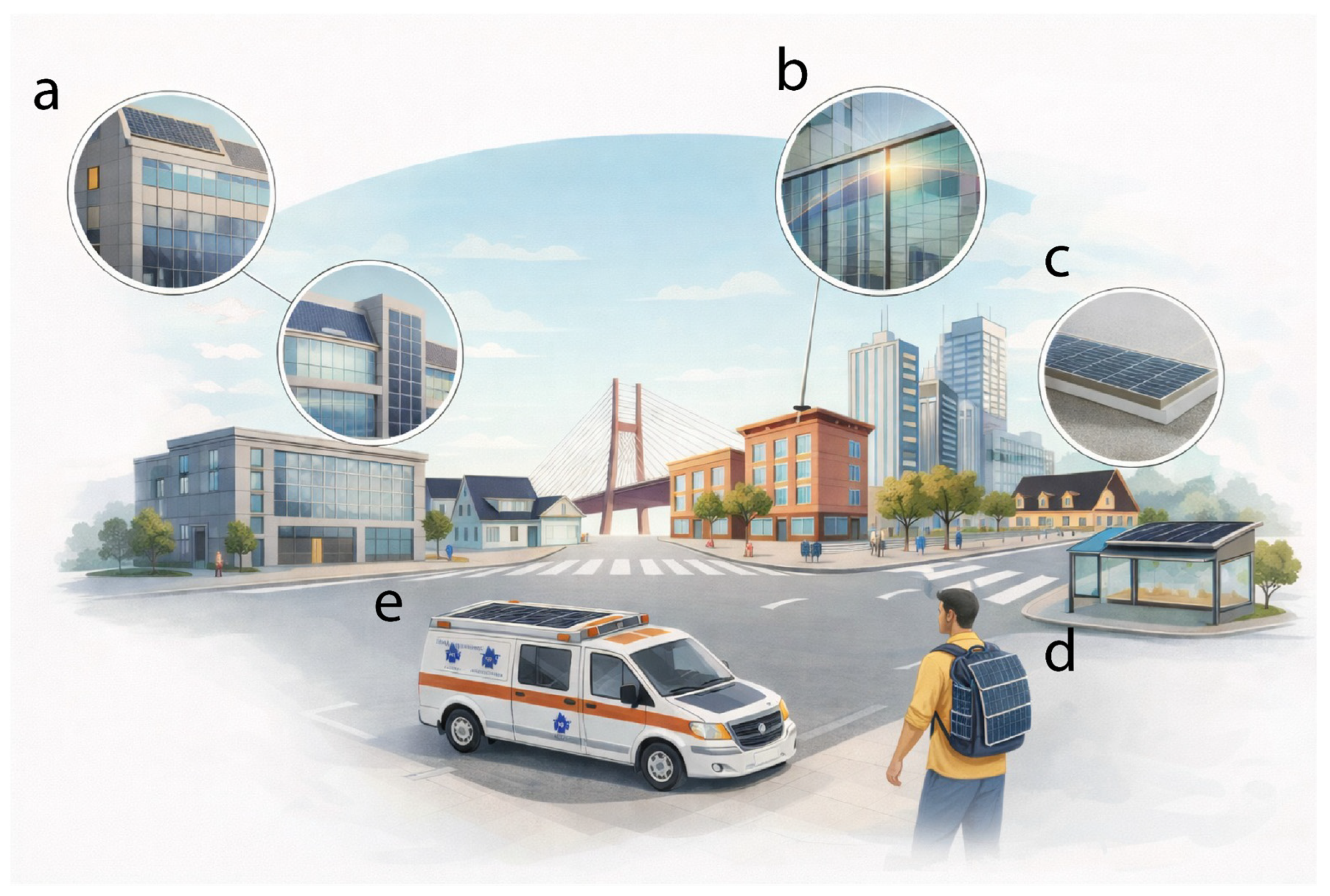
Figure 1. Illustration of photovoltaic integration on non-conventional substrates within urban and architectural environments. Different solar deployment platforms are represented, including (a) rooftop and façade integration on ceramic and building-derived substrates, (b) photovoltaic incorporation into glazed and transparent façade systems, (c) solar modules deposited on prefabricated rigid non-conventional surfaces, (d) flexible and wearable photovoltaic devices based on polymeric or elastomeric substrates, and (e) mobile applications on metallic substrates and vehicle-integrated structures.
Solar 06 00028 g001
Figure 2. (a) Schematic representation of different ionic diffusion pathways, where colored dots represent mobile ionic species or contaminants and red arrows indicate diffusion directions. (b) Schematic representation of open and closed porosity; red arrows indicate gas/vapor transport and outgassing pathways. (c) Schematic representation of tensile and compressive stress effects.
Solar 06 00028 g002
Figure 3. Cross-sectional view of a glazed ceramic tile for building envelope applications. The green box highlights the glaze layer, which constitutes the outermost functional surface for subsequent photovoltaic integration.
Solar 06 00028 g003
Figure 4. EDX line profile across the enamel, Mo/MoSe2, and CIGS layers, obtained from [112]. The colored curves correspond to the elemental profiles indicated in the original legend.
Solar 06 00028 g004
Figure 5. Schematic cross-section of a glazed ceramic substrate highlighting interdiffusion phenomena and surface defects.
Solar 06 00028 g005
Figure 6. Surface morphology of glazed ceramic substrates as revealed by AFM [112].
Solar 06 00028 g006
Figure 7. Reflectance spectra of matte (red) and polished (blue) ceramic substrates are shown in comparison with those of other reference substrates, namely glass (green) and stainless steel (grey).
Solar 06 00028 g007
Figure 8. Confocal microscopy images of the ceramic substrates showing (a) the matte surface and (b) the polished surface.
Solar 06 00028 g008
Figure 9. Schematic illustration of an Sb2Se3 solar cell fabricated on a ceramic tile substrate, together with a conceptual representation of building-integrated photovoltaic devices [104].
Solar 06 00028 g009
Figure 10. Defects arising from substrate impurity diffusion and their prevention by diffusion barriers [134].
Solar 06 00028 g010
Figure 13. Practical decision flowchart for selecting non-conventional substrates according to photovoltaic processing and application requirements.
Solar 06 00028 g013
Table 1. Different roughness regimes description and their main performance on solar cell device physics.
Length ScaleTypical Feature SizeDominant Impact on Solar DevicesRepresentative Consequences
Nanometric<10–20 nmNucleation, interfacial energetics, defect formationModified grain growth, trap density variation, interfacial recombination
Submicrometric20–500 nmLayer continuity, electric field homogeneityPinholes, local thinning, shunting when local features approach the thickness of critical functional layers
Micrometric0.5–50 µmDevice architecture constraintsMinimum layer thickness, need for planarization, optical losses, high risk of discontinuities in thin-film stacks.
Macroscopic/(waviness and geometric architecture)0.1 mm–cmProcessability, electric field and optical non-uniformityDeposition non-uniformity, edge effects, mechanical stress concentration
Table 2. Families of deposition mechanisms and their substrate common effects.
Technique Family (Examples)Growth-Limiting MechanismSensitivity to Substrate Chemistry *Dominant Substrate DriversTypical Integration ConstraintsScalability Potential *
Surface-reaction-limited deposition (ALD)Self-limiting surface reactionsVery highDensity and type of reactive sites (–OH, Lewis acidity/basicity), surface termination, contaminationNucleation delay, growth inhibition, non-uniform initial cycles, need for activation or seed layers, unfavorable film morphologyMedium.
Medium–High for Spatial ALD making process faster.
Solution nucleation-limited deposition (CBD, SILAR, hydrothermal)Heterogeneous nucleation and adsorption from solutionVery highSurface charge, acid–base character, wettability, complexation at the interfaceSuppressed or enhanced nucleation, bath-dependent variability, pinholes, strong sensitivity to cleaning and pre-functionalizationMedium. Scalable for batch or continuous processing on ceramics, metals and polymers.
Electrochemical reaction-limited deposition (electrodeposition, electroless plating)Interfacial electron transfer and surface catalysisHighElectrical conductivity, local potential distribution, catalytic activity, native oxide layersSelective growth or voids, adhesion failure, composition gradients, need for conductive seed layers or surface activationMedium–High. Highly scalable on conductive metals and metallized substrates.
Gas-phase surface-kinetics-limited deposition (CVD, MOCVD, PECVD)Gas-phase reactions and surface reaction kineticsIntermediate–HighSurface energy, catalytic activity, native oxides, functional groups, thermal stabilityNucleation delay on inert surfaces, parasitic interfacial reactions, thermal budget constraintsMedium. Industrially scalable on thermally stable materials.
Flux-limited physical condensation (PVD sputtering, e-beam evaporation, thermal evaporation, cathodic arc)Arrival rate and energy of incoming species; physical stickingLow–IntermediateSurface cleanliness, roughness, shadowing, temperature, mechanical complianceColumnar growth, poor step coverage on rough substrates, delaminationHigh. Widely scalable on glass, metals, ceramics and polymer foils.
Energetic ion-assisted deposition (IBAD, HiPIMS, plasma treatments)Energetic bombardment modifies the near-surface regionIntermediateSubstrate damage threshold, chemical modification, charging effectsDensification versus substrate damage, altered adhesion, induced defects, need for optimized process windowMedium. Useful for large-area surface activation or dense coatings.
Solution coating/wet-film formation (spin coating, doctor blade, spray coating)Wetting, flow and solvent evaporationIntermediateSurface energy, chemical compatibility, topography, absorption and porosityDewetting, thickness non-uniformity, coffee-ring effects, infiltration into porous substrates, need for surface control and barrier/planarization layersHigh. Particularly suitable for polymers, paper, textiles and roll-to-roll processing.
Printing with particulate inks (screen printing, inkjet, aerosol jet)Ink rheology, drying/sintering and percolationIntermediateSurface energy, porosity, ink uptake, roughness, thermal budgetPoor line definition, ink bleeding or infiltration, incomplete sintering on low-temperature substrates, mechanical cracking under strainHigh. Particularly suitable for polymers, paper, textiles and roll-to-roll processing.
* Sensitivity to the substrate chemistry and scalability potential is qualitative and depends on the deposition method, substrate geometry, thermal budget, roughness, porosity and the need for barrier or planarization layers.
Table 4. Chemical analysis of the enamels performed by XRF [112].
Alkali Content (wt.%)STDABCD
Na2O1.002.002.004.006.64
K2O1.004.204.603.202.20
Na2O + K2O2.006.206.607.208.84
Table 8. Key properties of representative polymeric substrates for flexible photovoltaics.
PropertyPETPENPolyimide (CPI)
Chemical familyAromatic polyesterAromatic polyesterAromatic imide
Glass transition temperature, Tg (°C)~70120–130>300
Maximum processing temperature (°C)~100~150>350
Optical transparency (%)~85~8580–90
Young’s modulus (GPa)2–44–52.5–3.5
Thermal stability (practical thermal endurance/heat resistance, °C)150–200150–200350–500
Water vapor transmission rates (WVTR) (bare film, ~100 µm) (g·m−2·day−1)~9~2~0.5–1
Typical photovoltaic useOPV, low-T PSCFlexible PSCHigh-performance PSC
Table 11. Key properties of paper and textile substrates used in photovoltaic applications.
PropertyPaper (Cellulose-Based)Polymer Textiles (Natural/Synthetic)Glass Fiber Textiles
Young’s modulus (GPa)~4.3 (nanofiber)/10–17 (laminates)~0.1–1>1 (significantly higher; typically tens of GPa)
Thermal degradation onset (°C)~300≤300 (natural fibers), lower for some>230 (stable under vacuum)
Glass transition (°C)NonePET: ~89None
Dimensional stability limit (°C)~300 (before degradation)~160 (onset of shrinkage for PET)Stable at 180–225 (PECVD conditions)
Coefficient of thermal expansion (CTE) (10−6 K−1)—High (mismatch with Si)~4 (close to Si)
Mechanical flexibilityHigh (foldable)HighLow
StretchabilityLowHigh (knitted structures)Negligible
Bending toleranceVery high (tight radii)HighLimited
Key processing implicationGood for low-T flexible processingLimited by thermal shrinkageCompatible with high-T processes (e.g., PECVD a-Si:H)
Table 13. Common physical constraints associated with each substrate-type.
ConstraintCeramicsMetalsPolymersPorous Substrates
Dominant roughness scaleµmsub-µmnm–µmmulti-scale (µm–mm)
Main diffusion speciesNa+, K+Fe, Cr, NiOrganics, additivesMulti-species
Thermal limitHighHighLow–moderateVariable?
CTE mismatch riskModerateSubstrate-dependentHigh (soft vs. brittle stack)High heterogeneity
PermeabilityLow–moderateVery lowHighVery high
Barrier necessityOften beneficialCriticalCriticalCritical
Table 14. Comparative performance and qualitative economic assessment of non-conventional photovoltaic substrates.
Substrate FamilyBest Efficiency Reported in This ReviewRecord Efficiency for Same PV TechnologyMain Substrate-Related BottleneckMost Suitable Application/Economic Rationale
Ceramics/Building-derived substrates14.28% CIGS on glazed ceramic tile23.64% CIGSGlaze roughness, surface defects, alkali diffusion control and need for surface conditioningBest suited for BIPV, façades and roofing elements, where the substrate already forms part of the building envelope and added PV functionality can offset processing costs
Metallic substrates17.9% CIGS on Ti foil; 12.6% CIGS on stainless steel23.64% CIGSElectrical conductivity, impurity diffusion, oxidation, CTE mismatch and need for dielectric/diffusion barriersAttractive for high-value lightweight or flexible systems such as aerospace, transport and portable modules, where robustness and thermal stability justify higher integration costs
Polymeric substrates18.7% CIGS on polyimide23.64% CIGSLow thermal budget, gas/moisture permeability, outgassing and mechanical fatigue of brittle layersStrong potential for low-cost flexible PV and roll-to-roll manufacturing, although barrier layers and encapsulation reduce part of the cost advantage
Paper/cellulose-derived substrates18.71% OPV on cellulose-derived substrate19.4% OPVHygroscopicity, roughness, permeability, dimensional instability and limited thermal stabilityPromising for low-temperature OPV/PSC, indoor PV, IoT and sustainable or disposable electronics, where low substrate cost and lightweight format are more relevant than long outdoor lifetime
Textile/fibrous substrates17.49% GaAs transferred to fabric; 5.72% PSC by direct deposition29.1% GaAs; ~27.3% PSCMultiscale roughness, weave topology, encapsulation, washability and trade-off between planarization and textile propertiesMost relevant for wearables, smart textiles and low-power energy harvesting, where mechanical integration and added functionality are more important than maximum energy yield
Disclaimer/Publisher’s Note: The statements, opinions and data contained in all publications are solely those of the individual author(s) and contributor(s) and not of MDPI and/or the editor(s). MDPI and/or the editor(s) disclaim responsibility for any injury to people or property resulting from any ideas, methods, instructions or products referred to in the content.