Abstract
We present our own Interdigitated Back Contact (IBC) technology, which was developed at ISC Konstanz and implemented in mass production with and at SPIC Solar in Xining, China, with production efficiencies of over 24%. To our knowledge, this is the highest efficiency achieved in the mass production of crystalline silicon solar cells without the use of charge-carrier-selective contacts. With an adapted screen-printing sequence, it is possible to achieve open-circuit voltages of over 700 mV. Advanced module technology has been developed for the IBC interconnection, which is ultimately simpler than for conventional double-sided contacted solar cells. In the next step, we will realize low-cost charge-carrier-selective contacts for both polarities in a simple sequence using processes developed and patented at ISC Konstanz. With the industrialisation of this process, it will be possible to achieve efficiencies well above 25% at low cost. We will show that with the replacement of silver screen-printed contacts by copper or aluminium metallisation, future IBC technology will be the end product for the PV market, as it is the best performing c-Si technology, leading to the lowest cost of electricity, even in utility-scale applications.
1. Introduction
The photovoltaic (PV) market is currently dominated by crystalline silicon (c-Si) p-type Passivated Emitter and Rear Contact (PERC) solar cell technology, as it offers a low-cost, high-efficiency process with average production efficiencies of around 23%. The module efficiencies available on the market are between 21–22% [1]. It has been a common understanding in the PV community for over one year now that PERC technology is coming to its efficiency limit, and n-type solar cell technologies will take over the PV market in the coming years. All new investments in and outside of China (except for the Indian market) are based on n-type technology—mostly on TOPCon (Tunneling Oxide Passivating Contacts) and HJT (Hetero Junction Technology). IBC (Interdigitated Back Contact) technology is the last technological step in all roadmaps of institutes and companies; however, it is believed to be complicated and costly, so it will be used for niche markets only. Besides the fact that niche markets, such as rooftops, building integration (BI) PVs, vehicle integration (VI) PVs and product integration (PI) PVs, are already at a large GW scale, low-cost IBC technology has the potential to become dominant in its bifacial configuration at the utility scale as well. The process has to be simplified, material usage reduced and Ag metallisation switched to Cu or Al. These are all topic we are addressing in a new European project “IBC4EU” with 17 partners having EUR 13.5 Mio. In funding coordinated by ISC Konstanz, starting from November 2022 [2].
Figure 1 on the left depicts the c-Si technology shares in the past and present and offers a possible forecast until 2030, redrawn from [3,4]. Ever since 2016, when a large Cz-Si ingot and wafer producer LONGi introduced low-cost Cz-Si wafers into the PV market, and, as a consequence, Al-BSF (Aluminium Back Surface Field) solar cell technology and, with it, mc-Si technology began to disappear from the PV market, innovative high-efficiency solar cell concepts have been on the rise. The reason for the fast decrease in the market share of Al-BSF was also because this technology came to its efficiency limits due to its low passivation ability on the rear side due to the BSF field effect. The next technological step was, therefore, the implementation of a passivated rear side by dielectrics, which leads to current average PERC voltages around 685 mV and 690 mV max. As the PV market is used to yearly enhancements of 0.5% absolute in efficiency, the next technological steps are to further reduce the contribution of recombination underneath the metal contacts, either by advanced screen printing or by the implementation of carrier-selective contacts leading to open-circuit voltages of above 700 mV.
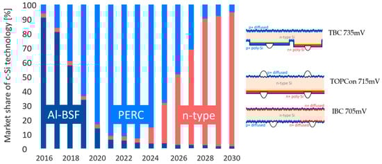
Figure 1.
Market share of Al-BSF, PERC and n-type solar cell technologies, redrawn from [3,4] (left) and cross sections of n-type technologies with no, one or two carrier-selective contacts with a 1 nm thin oxide layer (yellow line), leading to 705 mV, 715 mV or 735 mV, respectively (right).
Figure 1 on the right depicts cross sections of n-type solar cell technologies with no, one or two carrier-selective contacts, leading to average open-circuit voltages Voc of 705 mV, 715 mV or 735 mV, respectively. The carrier-selective contacts consist of an approximately 1 nm thin tunneling oxide (yellow line) between the c-Si bulk and poly-Si doped layer. The creation and proper contacting of the n-doped (phosphorous-doped) poly-Si layer are easier than those of the p-type (boron-doped), which is why n-type PERT concepts with n-type poly-Si rear sides are preferable to p-type PERT concepts, as the poly-Si layer is also highly absorbent when compared to a standard emitter. That is also the reason why a TBC (TOPCon Back Contact) is the perfect device, as both poly-Si layers are on the rear side. The metallisation switch from silver (Ag) to a lower conducting metal such as copper (Cu) and/or aluminium (Al) is easier, as this reduces the bifacial factor only, despite having a perfect front side. That is why all road maps of institutes and industry for c-Si solar cells end with an IBC device with a practical efficiency of 25–26%.
In the following sections, we will look at different possibilities of IBC solar cells in terms of process complexity, efficiency potential and costs. Figure 2 depicts the cross sections of three different major IBC solar cell concepts that are on the PV market already or in R&D at institutes or by industry.
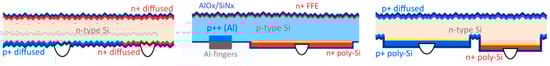
Figure 2.
Cross sections of 3 major different IBC cell concepts with no, one and two carrier-selective contacts. Red colour represents n-type doped regions, blue p-type doped and yellow a thin tunnelling oxide.
On the far left, the cross section shows a simple IBC solar cell concept (as, e.g., ZEBRA) that is totally diffused and has no carrier-selective contacts yet implemented, which is limiting, on the one hand, the voltage to about 705 mV; however, on the other hand, it is having a very lean process flow with stable and standard processes. In production, not only high efficiencies matter but also low COO (cost of ownership), high throughput and high yield. In addition, having both-sided diffusions underneath the passivation layers leads to a stable UV exposure behaviour from the front as well as from the front side [5], which has to be considered in field as well. At the end, the performance in the field is not only about record efficiencies but also about stability and behaviour at elevated temperatures.
Coming now to the structures with passivating contacts or, as mentioned often in the literature, as “carrier-selective contacts”, many machine builders such as Semco, Centrotherm, Schmid and Von Ardenne are currently very focused on the development of poly-Si deposition technologies with LPCVD, PECVD, APCVD and PVD systems in respect to one-sided deposition, in situ doping, low process times and high yield. Once the developments are successful, more and more devices with carrier-selective contacts will become visible on the market. In the middle, the so-called POLO IBC structure is depicted with the same process equipment as PERC, except for the carrier-selective contact with a thin oxide as well as a poly-Si deposition on the rear side. As the front side is passivated by dielectrics only, without having any diffusion beneath the passivation, it has a high efficiency potential; however, there is the potential for high UV degradation as well. On the far right, an ultimate IBC device with both carrier-selective contacts is shown, which has the highest efficiency potential of 25 + % on the solar cell level. As it is a combination of TOPCon and IBC technology, the PV community has started to call it TBC (TOPCon Back Contact) technology.
Table 1 summarises the most prominent IBC solar cell concepts in R&D and in the PV market. On the far left, there are three solar cell concepts without any passivating contact from SPIC/ISC, ipv Stuttgart and Jolywood. The ZEBRA IBC cell reaches 24% in production [6,7] and is about 80% based on standard PERC production, using the same equipment. The ipv concept MESA is based on selective laser-diffusions results, of 23.3% [8,9]. There is not much known about the IBC process from Jolywood—only that it is also not based on carrier-selective contact technology and that the P-diffusion is done by implantation. The costs of all three concepts are below 1.5 × PERC costs, which are shown the COO section for the case of ZEBRA. The POLO IBC technology by ISFH is using one carrier-selective contact and also still Al screen printing for the BSF formation. The efficiency for large area devices is at 21.8% [10], and the projected costs in production are also close to PERC. The IBC technologies with both passivating contacts currently have the highest efficiency and the highest costs, which makes them only attractive for high power-density markets such as rooftops.

Table 1.
Prominent IBC technologies on the market and their properties.
Figure 3 illustrates once more why there are different IBC concepts that coexist. Different institutes and companies have different strategies for upgrading their double-sided contacted solar cell architectures. LONGi and ISFH, staunch supporters of PERC technology, have developed a simple upgrade of PERC technology that ECN/TNO was proposing 5 years ago. ISC Konstanz, ipv Stuttgart and companies such as Jolywood, SPIC and Valoe are pursuing an upgrade of the nPERT technology and, thus, also IBC by further development to the TBC route. SunPower and Aiko have opted directly for TBC technology. There is still a fourth prominent path to IBC that is not shown here—HJT IBC. This was first demonstrated by Kaneka and is now being pursued by REC, Meyer Burger and ENEL.
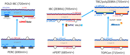
Figure 3.
Different structures of IBC solar cells as evolutions from different both-sided contacted solar cells.
2. ZEBRA IBC without Carrier-Selective Contacts
As already mentioned, the ZEBRA solar cell is the device with the highest efficiency in production that is not using any carrier-selective contacts. The modules on the market compete with concepts having one or two passivating contacts such as TBC (SunPower), HJT (REC) and TOPCon (Q-cells) [1]. The ZEBRA process flow, properties and future developments on the cell and module levels are described in detail as follows.
2.1. ZEBRA Process
Figure 4 shows the process flows of the main cell concepts that co-exist in the PV market. The market shares for PERC and n-type technologies are shown in Figure 1. There is no question that n-type technologies are replacing PERC technology. However, the question is which of the n-type concepts will take over the market leadership—TOPCon, HJT or IBC.
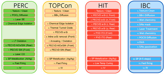
Figure 4.
Process flows for PERC, TOPCon, HJT and IBC.
If one judges by simplicity and the efficiency to be achieved, then HJT would win. This is also the deceptive aspect of a simple approach and aso a reason why some investors and newcomers opt for this concept. However, they have not taken into account the throughput, yield and complexity of the module concept. Even though TOPCon and IBC have a more complex process flow with 12 process steps, the robustness of the process and the possibility to use standard module processes is also the reason why all Tier1 PERC manufacturers such as Jinko, Q-cells, Trina and LONGi have chosen TOPCon. PERC, TOPon and IBC build on each other, so standard processes can be used.
The ZEBRA process, like the TOPCon process, consists of 12 steps involving only standard equipment such as wet chemistry, POCl3 and BBr3 diffusions, PECVD SiNx, laser treatment and screen printing [12]. The main advantages of ZEBRA are that no passivating contacts are used and that the passivation of the surfaces is done by the glass produced during diffusion, so no AlOx is needed on either side. This technology is very specific and has been developed and patented at ISC Konstanz [13]. Thanks to the use of thermal silicon oxide, a ZEBRA cell also shows an excellent behaviour of the reverse I-V characteristics compared to AlOx, which is deposited at low temperatures around 400 °C. As already mentioned, the combination of diffusion and additional passivation with BSG/SiNx and PSG/SiNx is also particularly UV stable [5]. No UV blockers have to be built into the module, but UV light can be used to generate electricity, which also contributes to the lower Levelised Cost of Electricity (LCOE), which will be explained later.
2.2. ZEBRA Characterics
From the point of view of the metallisation pattern, ISC Konstanz’s ZEBRA technology is basically not an IBC technology, but a 3D screen-printing technology where an insulating paste and the busbars are printed over the fingers. This technology is already known and is called “Floating Busbars”. However, we have developed this technology further by using an insulating paste. Reverse screen printing is, therefore, more complex than that for PERC or TOPCon technology. However, there are more degrees of freedom in terms of the amount and type of material applied than on the front side of PERC, TOPCon and HJT.
Figure 5 shows pictures (left, centre) and the schematic drawing of the described metallisation. This technology is suitable for making the number of busbars very flexible. In the meantime, the solar cells in production are very thin busbars in order to save silver. The following sections discuss the efficiencies achieved in production and further describe the developments.
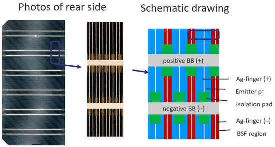
Figure 5.
Picture of the back side of a four-busbar ZEBRA solar cell (left, middle) and schematic drawing of the back-side metallisation of ZEBRA (right) [13].
2.3. ZEBRA in Production
Since 2020, the company SPIC Solar in Xining, China, has been producing ZEBRA solar cells with a capacity of 200 MW annually. The efficiency has been steadily increased, and the silver consumption has been reduced over the last 2 years. Figure 6 shows the parameters from a weekly cell production in April 2022 for the whole distribution and as a daily average. These solar cells were produced on M6 substrates (166 × 166 mm2 with a diagonal of 223 mm2) with an initial thickness of 170 µm using six-busbar technology.
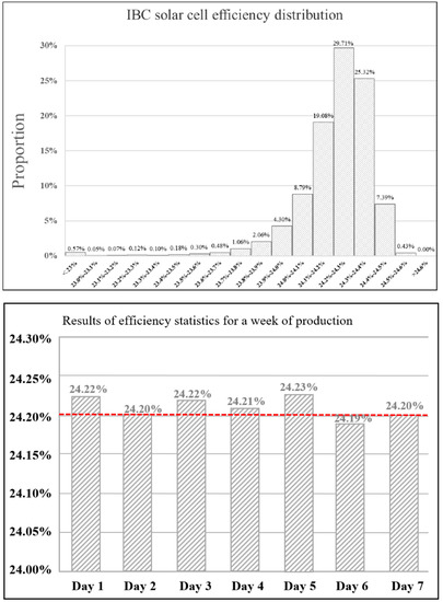
Figure 6.
Distribution of IV data for all solar cells (top) and average on daily basis (bottom) for a week of production in April 2022.
The daily average is always above 24%, and the average is very stable at 24.2%. Table 2 shows the average parameters over the whole week and the parameters of the best solar cell.
Table 2.
Average IV data and best cell performance for a week of production in April 2022.
The best solar cell has an open terminal voltage of 704 mV and an efficiency of 24.6%, which marks the new world record for a solar cell in production without passivating contacts.
2.4. ZEBRA with Copper and Aluminium Contacts
The biggest challenge for all n-type technologies is to minimise or even replace silver metallisation, which is almost twice as large for PERC solar cells with a back contact metallisation that consists of fired Al paste. Some institutes are trying to do this by plating Cu contacts, but plating is a very complex technology, and the disposal of the chemicals is not very easy. On the other hand, screen-printing technology offers a very robust process that is far from being exhausted. Due to the continuous development of screens and printing pastes, finer and finer lines can be printed, and higher-resistance emitters can be contacted. In addition, screen printing offers the simplest method of selectively printing on surfaces without having to use masks.
Therefore, we have been developing alternative printing technologies with special screens and metal pastes such as Cu and Al for several years. The cooperation of the company Copprint has led to excellent results in contacting ZEBRA cell medium copper pastes, which have been specially adapted for this purpose.
Figure 7 shows, on the left side, the cross-section of a silver and copper screen-printed finger and, on the right side, the backside of the entire M6 ZEBRA solar cell in the four-busbar configuration. The special feature is that only 40 mg silver was printed for the entire solar cell (<5 mg silver/Wp)—which is about half the silver metallisation of PERC. The cell parameters are summarised in Table 3, and, in the experiment, they correspond to the parameters of the reference cell that was only metallised with silver, except for the fill factor, which could be improved.
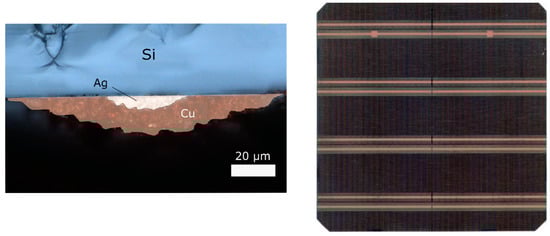
Figure 7.
Cross sections of Ag/Cu-metallised finger contact (left) and Cu-metallised M6 4BB ZEBRA solar cell (right).
Table 3.
IV data of fully Ag-printed (reference) and Cu-printed ZEBRA solar cells with the same geometry (G1 wafer, 4BB) [14].
The efficiencies are generally at a worse level than in production because of the laboratory process and the poorer-quality n-type substrates. The voltages, therefore, ran below 700 mV, but the essence of the experiment was that they were at a similar level. The only lower value is the fill factor, which will be optimised in the future. The wider print reduces the bifacial factor from 0.74 to 0.65, but the cost of the solar cell is greatly reduced by saving the silver. Module tests with the Cu cells in climatic chambers showed no higher degradation than those for the Ag cells, and, thus, an in-diffusion of copper into the silicon can be excluded [14,15]. The only property that still needs to be significantly improved is the adhesion of the copper fingers and busbars. This is currently being worked on with Copprint. Even if the further experiments are successfully completed, it will still take a long time for the Cu screen-printing technology to become established, because the desire of the PV industry to replace Ag is not yet great enough, compared to the fear that the Cu ZEBRA modules will degrade in the field. The bankability needs to be worked on for up to 3 years.
3. ZEBRA IBC with Carrier-Selective Contacts
ZEBRA technology leads to high open-clamp voltages of over 700 mV. However, 705 mV is the limit for this technology without passivating contacts. To reach open terminal voltages of over 720 mV and later even over 735 mV, both polarities must be passivated. There are various approaches for poly-Si deposition as well as for the structuring of the selective deposition of these layers. We have had very good experience with laser technology in recent years and, therefore, use it for the development of our so-called “poly-ZEBRA” (TBC). The laser processes are used to dope and densify the poly-Si layers, so they remain resistant to certain etching processes.
Figure 8 shows, on the left side of the image in the middle, such a layer (light area) surrounded by etched layers (dark areas). On the right side of Figure 8 is the cross-section of such a structure.
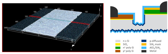
Figure 8.
Laser-scanning micrograph of a surface of the laser-densified boron-doped poly-Si layer (light area) surrounded by etched layers (dark areas) (left) and cross-section of the poly-ZEBRA (TBC) structure (right).
We cannot disclose the exact process flow, as this sequence and the exact method are patent-pending. The finished solar cells already clearly show the higher voltages in the brighter areas of the TBC solar cell under electroluminescence images as shown in Figure 9.
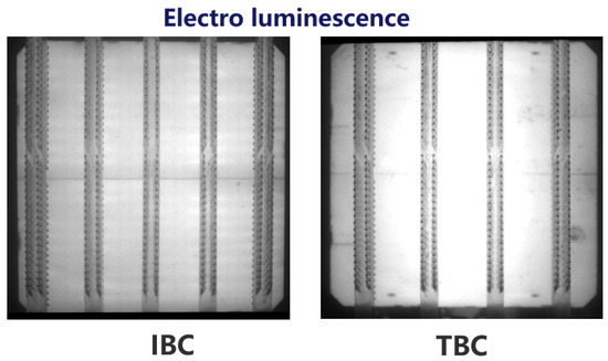
Figure 9.
Electroluminescence images of IBC (reference) and TBC solar cells processed in the same experiment.
Table 4 shows the average values from the experiment at SPIC. The increase in the open terminal voltage is clearly visible.
Table 4.
Average IV data for IBC and TBC processes for 50 solar cells each.
Further experiments to improve the TBC properties are mainly aimed at simplifying the process and increasing the filling factor. With the TBC process, efficiencies of over 25% are possible.
4. ZEBRA Modules
One of the reasons why the PV community has doubts about the breakthrough of IBC technology is the belief that the classic ribbon-based stringing of IBC solar cells is difficult. This is because stringing on only one side leads to severe bending of the solar cells. However, with the introduction of half-cell technology and minor adjustments to the stringing process, the interconnection of IBC solar cells is straight-forward. The adapted interconnection process enables industrial string fabrication based on solder-coated copper ribbons at similar throughputs, as for both-sided contacted solar cells.
Figure 10 shows, on the left side, the bowing of the ZEBRA half-cells in the string matrix is within an acceptable range (<2 mm). On the right side, the so-called “Negative Gap Technology” is shown from a top view. Here, neighbouring half cells are slightly overlapped to form a continuous string of half cells, without any cell-to-cell gaps increasing the active module area. In this way, and through the interconnection with narrow solder ribbons, very homogeneous bifacial ZEBRA modules can be produced from the front side, as shown in Figure 11.
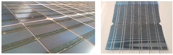
Figure 10.
Interconnection of ZEBRA half cells (left) and “Negative Gap Technology” at IBC (right).
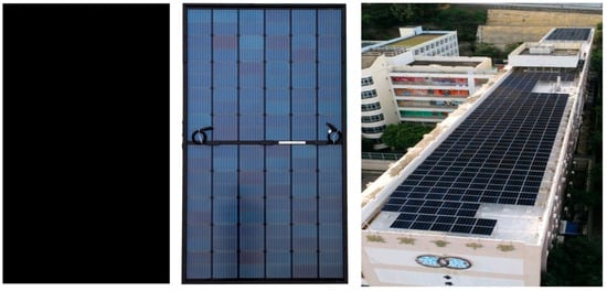
Figure 11.
Pictures of bifacial ZEBRA module (ANDROMEDA2.0 by SPIC) from the front and back (left) and application in Hong Kong on a flat roof (right).
Since bifacial ZEBRA (ANDROMEDA2.0) modules have not yet reached their minimum cost, they will be used for roof applications for the time being. In the future, however, further-developed poly-ZEBRA modules can also be used in large PV power plants. The cost calculations for this are explained in the next section.
5. COO and LCOE
In the present section, we present the results of calculations performed using a bottom-up cost model developed at ISC Konstanz [16], based on the process flows currently implemented in industry for PERC, TOUCAN (ISC’s TOPCon route) and ZEBRA as well as on the anticipated process flow for poly-ZEBRA. The cost structure—i.e., the assumptions for the cost of labour, energy, building, facilities and raw materials—corresponds to the scenario of an integrated cell and module factory located in a low-cost Asian country with a yearly manufacturing capacity of 5 GWp. The wafer cost has been determined based on a poly-silicon cost of USD 15/kg. This is assumed to be the market price in a situation where the supply and the demand of poly-silicon are balanced. The resulting wafer cost is USD 0.61/wafer for p-type Cz-Si M10 (182 mm × 182 mm) wafers and USD 0.664/wafer for n-type Cz-Si M10 wafers. The cost of the Ag-pastes has been calculated for a cost of pure Ag of USD 700/kg. The resulting cost of ownership (COO) for the manufacturing of the different cell technologies is shown in Figure 12.
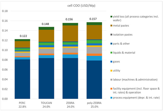
Figure 12.
COO of different solar cell technologies and their energy-conversion efficiencies.
In the subsequent step, the calculated COO values for the cells have been used to determine the module’s COO for a module size of 144 half cells (M10). Based on the assumptions for the raw materials, the cost for the bill of materials (excluding cells, BOM) is USD 43/module. In addition, a cell-to-module Pmpp loss of 0% has been assumed for all cell technologies, a value that can be reached when using white reflectors in the cell interspaces for bifacial modules or a white backsheet for monofacial modules.
The resulting module manufacturing cost is shown in Figure 13. As can be noticed, thanks to the high Pmpp of the poly-ZEBRA module (with 25.5% cell efficiency), although the cell cost is the highest amongst the technologies investigated here, the anticipated module production cost is already lower than the cost calculated for the current ZEBRA technology (24% cell efficiency).
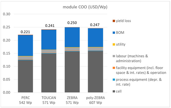
Figure 13.
COO of different module technologies and Pmpp (Wp) at STC for a 144 half-cell module using the respective cell technologies.
The above calculated results in terms of module power for 144 half-cell (M10) modules, with the respective cell technologies as well as the respective module cost (USD/Wp), have been used as input for calculating the levelised cost of electricity (LCOE) for a fixed-tilt, ground-mounted, utility-scale PV system located in Malaga (Spain). The main assumptions used for the LCOE calculations are summarised in Table 5 and Table 6. The results of the LCOE calculations based on these assumptions are shown in Figure 14.
Table 5.
General assumptions for LCOE calculations.
Table 6.
Technology specific assumptions for LCOE.
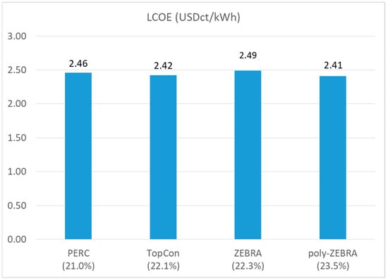
Figure 14.
Result of LCOE calculations for different bifacial technologies; the module efficiencies for the respective cell technologies are indicated in brackets.
As a result, amongst the technologies that are currently implemented in mass production, for the scenario of a ground-mounted, utility-scale system in a rather hot climate with high ground albedo, TOUCAN/TOPCon can reach the lowest LCOE, while electricity production by PERC and ZEBRA is slightly more costly. On the other hand, the LCOE calculations show that, thanks to the high module efficiency and to the high specific yield due to the low temperature coefficient and the related savings in the area-related balance of the system cost, a PV system based on poly-ZEBRA modules is anticipated to reach an LCOE that is even lower than the current values achieved by TOPCon.
6. Conclusions
ZEBRA technology is currently almost the only IBC technology in the PV market and the only technology that can reach open-clamp voltages Voc of over 700 mV without passivating contacts. Currently, ZEBRA is used for rooftop applications, BIPV and VIPV, but the first systems with bifacial ZEBRA modules for utility scale are emerging. Further developments, such as the implementation of copper and aluminium metallisation as well as poly-Si, qualifies poly-ZEBRA technology and other TBC technologies to be able to become the most important technologies on the market in 5–7 years. By increasing module efficiency to more than 23%, while reducing the COO and the temperature coefficient, the lowest LCOEs will be achieved. ISC Konstanz is working towards this goal, as the coordinator of the large EU project “IBC4EU”, with 16 other partners from R&D and especially from industry. With the bifacial poly-ZEBRA technology, large production capacities are to be created in Europe. In order to achieve this goal together, ISC Konstanz is organising a back-contact workshop with two other German institutes, ISFH and FhG ISE, and an institute from the Netherlands, TNO: www.backcontact-workshop.com (accessed on 21 December 2022).
Author Contributions
Conceptualisation, R.K. and P.D.; methodology, F.B. and V.D.M.; validation, F.B., V.D.M., J.L. (Joris Libal), Y.G., X.Q., X.W. and J.G.; formal analysis, F.B., V.D.M. and J.L. (Joris Libal); investigation, F.B., V.D.M., J.L. (Joris Libal), J.L. (Jan Lossen), N.C., H.C., C.P., T.T., A.H., Y.G., X.Q., X.W. and J.G.; data curation, F.B., V.D.M. and J.L.; writing—original draft preparation, R.K. and J.L. (Joris Libal); writing—review and editing, R.K. and J.L. (Joris Libal); supervision, F.B. and V.D.M.; project administration, F.B., V.D.M., J.L. (Joris Libal) and J.L. (Jan Lossen); funding acquisition, R.K., F.B. and P.D. All authors have read and agreed to the published version of the manuscript.
Funding
This work was funded by the German Federal Ministry for Economic Affairs (BMWi) with several projects such as Nexttec-03EE1001B, Zquadrat-03EE1005A, FlexFab2-03EE1081B and own developments by ISC Konstanz.
Institutional Review Board Statement
Not applicable.
Informed Consent Statement
Not applicable.
Data Availability Statement
Data is available at SPIC and ISC Konstanz.
Acknowledgments
We thank all the dedicated and hardworking process engineers of ISC Konstanz and LONGi Solar for providing the high-quality n-type Cz-Si wafers.
Conflicts of Interest
The authors declare no conflict of interest.
References
- Clean Energy Reviews: Most Efficient Solar Panels. 2022. Available online: https://www.cleanenergyreviews.info/blog/most-efficient-solar-panels (accessed on 10 October 2022).
- EU Funding for the Mass-production of Highly Efficient IBC Solar Cells. Available online: https://www.german-energy-solutions.de/GES/Redaktion/EN/News/2022/20220720-EU-funding-IBC-cells.html (accessed on 10 October 2022).
- N-Type Technology Cycle to Dominate PV Industry Spending from 2024. Available online: https://www.pv-tech.org/n-type-technology-cycle-to-dominate-pv-industry-spending-from-2024/ (accessed on 10 October 2022).
- Forecast on Technology Shares. Available online: https://www.infolink-group.com/ (accessed on 10 October 2022).
- Sinha, A.; Qian, J.; Moffitt, S.L.; Hurst, K.; Terwilliger, K.; Miller, D.C.; Schelhas, L.T.; Hacke, P. UV-induced degradation of high-efficiency silicon PV modules with different cell architectures. Prog. Photovolt. Res. Appl. 2022, 31, 36–51. [Google Scholar] [CrossRef]
- Kopecek, R.; Libal, J.; Lossen, J.; Mihailetchi, V.D.; Chu, H.; Peter, C.; Buchholz, F.; Wefringhaus, E.; Halm, A.; Ma, J.; et al. ZEBRA technology: Low cost bifacial IBC solar cells in mass production with efficiency exceeding 23.5%. In Proceedings of the 47th IEEE Photovoltaic Specialists Conference (PVSC). IEEE, Calgary, AB, Canada, 15 June–21 August 2020; pp. 1008–1012. [Google Scholar] [CrossRef]
- Qu, X.; Wu, X.; Guo, Y.; Lin, M.; Dong, P.; Jan, L.; Valentin, D.; Joris, L.; Chu, H.; Peter, C.; et al. Industrial Production of High Efficient ZEBRA IBC Cells and Modules, In Back Contact Workshop, Munich 2022. Available online: https://www.backcontact-workshop.com/pdf/2022-1/9_SPIC.pdf (accessed on 10 October 2022).
- Dahlinger, M.; Carstens, K.; Hoffmann, E.; Zapf-Gottwick, R.; Werner, J.H. 23.2% laser processed back contact solar cell: Fabrication, characterization and modeling. Prog. Photovolt. Res. Appl. 2017, 25, 192–200. [Google Scholar] [CrossRef]
- Zapf-Gottwick, R.; Seren, S.; Fernandez-Robledo, S.; Wete, E.-P.; Schiliro, M.; Hassan, M.; Mihailetchi, V.; Buck, T.; Kopecek, R.; Köhler, J.; et al. Solar Cells with Laser Doped Boron Layers from Atmospheric Pressure Chemical Vapor Deposition. Solar 2022, 2, 15. [Google Scholar] [CrossRef]
- Dullweber, T.; Mertens, V.; Stöhr, M.; Langlois, J.; Mettner, L.; Baumann, U.; Haase, F.; Brendel, R.; Libal, J.; Hähnel, A.; et al. Towards cost-competitive high-efficiency POLO IBC Solar Cells with minimal conversion invest for existing PERC+ production lines. In Proceedings of the 8th World Conference on Photovoltaic Energy Conversion (WCPEC), Milan, Italy, 26–30 September 2022; pp. 35–39. [Google Scholar] [CrossRef]
- Trina Solar Takes n-Type Mono IBC Cell to Record 25.04% Conversion Efficiency. Available online: https://www.pv-tech.org/trina-solar-takes-n-type-mono-ibc-cell-to-record-25-04-conversion-efficienc/ (accessed on 10 October 2022).
- Galbiati, G.; Chu, H.; Mihailetchi, V.D.; Libal, J.; Kopecek, R. Latest Results in Screen-Printed IBC-ZEBRA Solar Cells. In Proceedings of the 7th World Conference on Photovoltaic Energy Conversion (WCPEC), Waikoloa, HI, USA, 10–15 June 2018; pp. 1540–1543. [Google Scholar] [CrossRef]
- Mihailetchi, V.D.; Chu, H.; Lossen, J.; Kopecek, R. Surface passivation of boron-diffused junctions by a borosilicate glass and in situ grown silicon dioxide interface layer. IEEE J. Photovolt. 2018, 8, 435–440. [Google Scholar] [CrossRef]
- Chen, N.; Rudolph, D.; Peter, C.; Zeman, M.; Isabella, O.; Rosen, Y.I.; Grouchko, M.; Shochet, O.; Mihailetchi, V.D. Thermal stable high efficiency copper screen printed back contact solar cells. Sol. RRL 2022, in press. [Google Scholar] [CrossRef]
- Rudolph, D.; Farneda, R.; Timofte, T.; Halm, A.; Chen, N.; Libal, J.; Buchholz, F.; Rosen, I.; Grouchko, M.; Shochet, O. Screen printable, non-fire-through copper paste applied as busbar metallization for back contact solar cells. AIP Conf. Proc. 2022, 2709, 020006. [Google Scholar] [CrossRef]
- Eiermann, F. Bottom-Up COO-Modell für Solarzelltechnologien. Master’s Thesis, HTWG Konstanz, Konstanz, Germany, 2021. [Google Scholar]
Disclaimer/Publisher’s Note: The statements, opinions and data contained in all publications are solely those of the individual author(s) and contributor(s) and not of MDPI and/or the editor(s). MDPI and/or the editor(s) disclaim responsibility for any injury to people or property resulting from any ideas, methods, instructions or products referred to in the content. |
© 2022 by the authors. Licensee MDPI, Basel, Switzerland. This article is an open access article distributed under the terms and conditions of the Creative Commons Attribution (CC BY) license (https://creativecommons.org/licenses/by/4.0/).