Article

Gallium Nitride High-Electron-Mobility Transistor-Based High-Energy Particle-Detection Preamplifier

1
Department of Physics, Ariel University, Ariel 40700, Israel
2
Department of Electrical Engineering, Ariel University, Ariel 40700, Israel
3
Department of Life and Physical Sciences, Physics Division, Fisk University, 1000 17th Avenue North, Nashville, TN 37208, USA
*
Author to whom correspondence should be addressed.
Metrology 2025, 5(2), 21; https://doi.org/10.3390/metrology5020021
Submission received: 20 November 2024 / Revised: 24 March 2025 / Accepted: 28 March 2025 / Published: 3 April 2025

Abstract

:
GaN High-Electron-Mobility Transistors have gained some foothold in the power-electronics industry. This is due to wide frequency bandwidth and power handling. Gallium Nitride offers a wide bandgap and higher critical field strength compared to most wide-bandgap semiconductors, resulting in better radiation resistance. Theoretically, it supports higher speeds as the device dimensions could be reduced without suffering voltage breakdown. The simulation and experimental results illustrate the superior performance of the Gallium Nitride High-Electron-Mobility Transistors in an amplifying circuit. Using a spice model for commercially available Gallium Nitride High-Electron-Mobility Transistors, non-distorted output to an input signal of 200 ps was displayed. Real-world measurements underscore the fast response of the Gallium Nitride High-Electron-Mobility Transistors with its measured slew rate at approximately 3000 V/μs, a result only 17% lower than the result obtained from the simulation. This fast response, coupled with the amplifier radiation resistance, shows promise for designing improved detection and imaging circuits with long Mean Time Between Failure required, for example, by next-generation industrial-process gamma transmission-computed tomography.

1. Introduction

X-ray microscopy and Computed Tomography (CT) are applied in metrology, with its metrological resolution limited by a dimensional measurement chain, which includes radiographic imaging [1]. The imaging resolution depends on detector pixel resolution and its point spread function but is physically limited to the order of 10 nm even at very short wavelengths [2,3,4]. Within the X-ray wavelength range between λ 1 pm to λ 10 nm is hard radiation (1 pm λ 100 pm), a range that overlaps with gamma radiation. Hard radiation penetrates material more than what is considered soft radiation (in the wavelength range of 0.1 nm λ 10 nm) and is the reason for applying hard radiation [4]. Fast gamma 2D and 3D (CT) imaging for metrology requires high-speed circuits with a high signal-to-noise ratio (SNR), which does not degrade and fail due to the radiation. While the development of detector materials is shifting to self-healing materials [5], current preamplifiers are silicon-based transistors prone to radiation damage. In order to address this drawback, preamplifier circuits are located at a distance from the detector matrix with shielding, which complicates the design and increases the circuit capacitance, leading to lower bandwidth and lower sensor data throughput. A solution to silicon-based preamplifier drawbacks suggested in this work is GaN-based amplifiers. GaN has been applied in power electronics as a replacement for Si-based MOSFETs (Metal Oxide Semiconductor Field-Effect Transistors). It has a wider band gap and higher mobility, i.e., lower resistance, and it provides lower power dissipation, increasing its power handling compared to Si-based MOSFETs. Two additional advantages, which have not been investigated, are its higher radiation-damage threshold and its faster switching times. A high radiation-damage threshold increases the component reliability in space and in nuclear detectors. A GaN FET (Field-Effect Transistor) placed at the input stage of a radiation detector can result in improved sensitivity and time resolution. Table 1 displays a comparison of some important properties regarding Si, SiC, and GaN.
The thermal conductivity κ of GaN is lower than Si and SiC. This means that GaN has lower power dissipation, limiting it to lower voltages if used for power devices. Compensating for it is the high-mobility μ , which, compounded with a high-charge (electron) carrier concentration, results in high conductivity and low resistance. In the specific case of detectors, the band gap E G , critical field strength E C , and mobility μ are the dominating factors for an appropriate material. Thermal conductivity κ is less of a concern as not much heat dissipation is expected. Table 1 indicates that excluding thermal conductivity, GaN properties promise superior performance for high voltage fast switching of detectors.

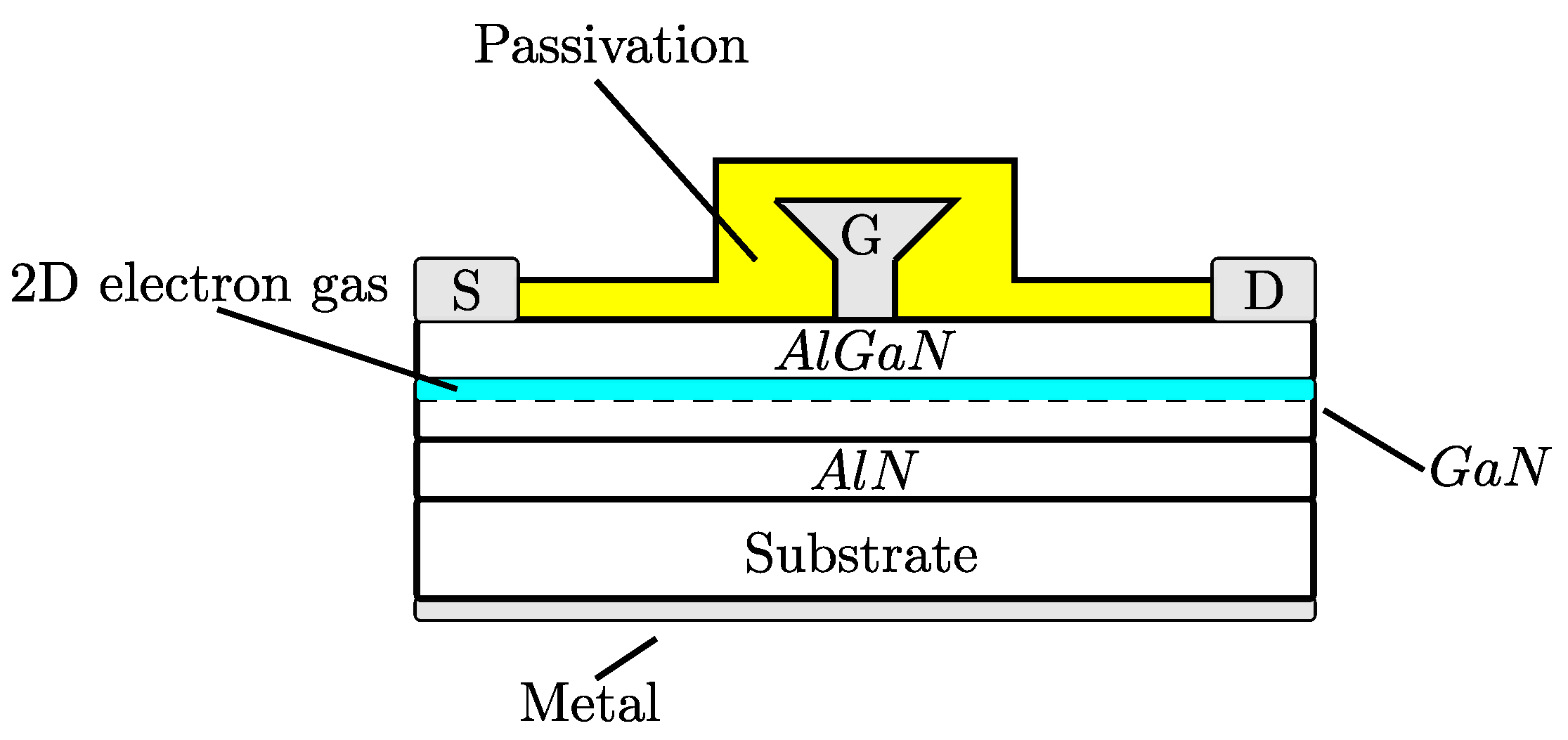
1.1. High-Electron-Mobility Transistor

GaN’s frequency performance can be improved by adopting a heterostructure containing layers of AlGaN and GaN (similar to modulation doping in GaAs [11]). The two different semiconductor layers have a gate that consists of a metal-semiconductor Schottky diode with regular contacts for drain and source (Figure 1).
Figure 1 illustrates a basic GaN High-Electron-Mobility Transistor (HEMT) transistor structure. The transistor heterostructure is placed on a substrate of either SiC or Si. An AlN buffer or nucleation layer is deposited on the substrate. On top of the AlN layer, a GaN layer is deposited. The GaN layer acts as the FET channel. An AlGaN barrier layer is deposited on top of the GaN layer, forming a heterojunction. The heterojunction offers an important advantage as charge carriers are increased considerably without introducing dopant impurities and without degrading the mobility. This structure has a unique property, in which charge carriers accumulate on the asymmetric junction formed between the two semiconductors with different band structures, confining them to the interface and creating what is known as a Two-Dimensional Electron Gas (2DEG). Transistors consisting of those structures are known as High-Electron-Mobility Transistors, theoretically showing promise of cutoff frequencies up to the THz range. Nitrides have a wurtzite crystal structure, which has a lower symmetry and hence built-in polarization. When growing AlGaN on a GaN layer, the AlGaN is stressed, creating piezoelectric polarization as it has a wider lattice structure than GaN. This adds to the spontaneous polarization built into the unstrained crystal, resulting in a sheet of uncompensated positive charge at the interface. Thus, a quantum well is created at the interface, leading to carrier confinement and a 2D electron gas in the undoped material as well as the doped one. This structure is superior to doped semiconductors such as GaAs and InP, in which the doping itself is responsible for ionized impurity scattering, reducing mobility. The 2D electron gas in GaN has a sheet charge density of the order of 10 13 cm−2, which is five times larger than a similar HEMT device using GaAs/AlGaAs. For a more detailed discussion, please refer to [12,13]. At this point, it is time to place a distinction between small-signal HEMTs, which are important for this current discussion, and HEMTs used in high-frequency power switching. Current small-signal devices begin at frequencies above 40 GHz, while most of the available work discusses power devices with larger gate lengths (>0.5 μ) and larger device cross-sections with lower cutoff frequencies. The higher breakdown voltage of the GaN (Table 1) contributes to even smaller devices and gate sizes improving performance at high frequencies.

1.2. Operating Frequency

High capacitance and low impedance are directly related to the transistor operating frequency. Increasing the cross-section of the device increases its capacitance, as the capacitance is proportional to the area of the conductors. This also reduces the impedance for the current increases ( z = v / i ). Thus, for our purposes, two frequencies characterize the device, namely the Gain Bandwidth Product (GBP) and the maximum frequency of oscillation f m a x .
G B P = g m 2 π C g s
f m a x = G B P 2 R d s R g
where g m is the transconductance, C g s the capacitive coupling between the gate and channel, R d s a resistance modeling the drain-source current, and R g the gate resistance. The GBP is the frequency in which the short circuit current gain falls to unity, while f m a x is the frequency in which the power gain falls to unity. The higher those values are, the higher performance the device provides at higher frequencies. If the area of the device is larger, it will increase the gate-source capacitance C g s , reducing the GBP (Equation (1)). This, in turn, will affect the maximum frequency (Equation (2)), reducing R d s , which depends on the device area as well. Thus, reducing the dimensions inherently increases the operating frequencies. One property of the material that affects the frequencies is the dielectric constant, as
C = ε 0 ε r A d
A lower dielectric constant results in lower capacitive loading, increasing the operating frequency. Table 2 compares the dielectric constant of several semiconducting materials.
As can be seen, GaN is favorable to other semiconducting materials, excluding diamond. In the GaN HEMTs, the gate consists of a Shockley diode, further reducing the gate–channel capacitive coupling. Table 1 shows that both electron mobility and electron saturation velocity are higher in GaN than in SiC and Si. This positions it as the better material for high-frequency solid-state devices. Polarized HEMT structure, which is currently commercially unique to GaN, has much higher mobility compared to other materials, including GaAs with a similar structure. It has a wider bandgap compared to GaAs, improving its reliability in environments with energetic radiation. GaN features a considerably lower noise figure [15], placing it as an attractive replacement in the first stage of the preamplifier.
To acquire some idea of the frequencies involved, some recent work should be referenced. Kabouche et al. reported an AlN/GaN HEMT with a maximum frequency f m a x = 242 GHz [16], with Li et al. reporting a cutoff frequency, GBP of 204 GHz and maximum device frequency of f m a x = 250 GHz [17]. This follows the work done by Y. Durmus obtaining GBP of 100 GHz and f m a x = 128 GHz using AlGaN/GaN. While this displays frequencies nearing the THz range, available commercial devices that are designed mostly for power amplification are available for cutoff frequencies of up to 20 GHz, such as work by Kim et al. with devices attaining GBP of approximately 19 GHz and f m a x of 60 GHz [18]. Kumar et al. report that using a FinFET structure, GaN devices obtain a GBP of approximately 2 THz [19].

2. Materials and Methods

Circuit design was undertaken using the open-source KiCAD suit. A simulation was carried out in LTspice. Figure 2 illustrates the component layout of the JFET-NMOS preamplifier. The printed circuit boards were fabricated based on the different designs, and the components were soldered to them.
The input and output signals are connected via SMA connectors. The different transistors incorporated into the various circuits are as follows:
2N4416
Si N-channel JFET high-frequency wide-bandwidth transistor. The transistor is designed to provide high performance and gain at high frequencies. It is supplied by Vishay Siliconix. For the full data sheet, please see reference [20].
2N3904
Si General purpose transistor. The transistor is a Si NPN bipolar junction transistor featuring high gain and low saturation voltage. It is supplied by multiple manufacturers, including OnSemi, NXP, and ST. For the full data sheet, please see reference [21].
2N7000
Small-signal MOSFET. The N-channel enhancement-mode field-effect transistor is designed with low on-state resistance, high frequency, and fast switching times. It is supplied by multiple manufacturers, including OnSemi, NXP, and ST. For the full data sheet, please see reference [22].
EPC2038
Enhancement-mode high-frequency GaN FET. This specific GaN transistor provides exceptionally low on-state resistance due to its structure featuring very high switching frequency and very low switching times. It is manufactured by the Efficient Power Conversion Corporation and, among its offerings, is one of the smallest structures and fastest switching times. For the full data sheet, please see reference [23].
The PCB was a standard FR-4 glass fiber-reinforced epoxy with copper-clad laminate. Resistors consisted of 5% carbon film 1/4 W through hole resistors, and the capacitors are 100 pF high frequency through hole disc capacitors [24].

GaN HEMT and Silicon JFET Detection Circuits (Preamplifiers)

The conventional way of sensing the γ -ray energy consists of using a JFET transistor (2N4416) as a source follower at the first stage, tracing the voltage of the charge generated by the interaction with the γ photon and the detector. JFETs are used due to their speed, low noise, and high input impedance. A simple detection circuit, based on [25], is illustrated in Figure 3.
In the above circuit, the HV bias controls the sensitivity of the circuit at times, requiring the use of a second amplification stage consisting of the 2N3904 transistor. While the first-stage transistor has a switching speed of 2.5 ns, the actual measured time resolution at its output is approximately 20 ns. The switching speed of the second general small-signal amplifying transistor is approximately 250 ns, providing a larger signal (small-signal amplification) at the expense of the time resolution. This is followed by an amplifier with the provisions of shaping the signal obtained from the preamplifier. For pulse-height spectroscopy, an A/D and a multichannel analyzer are connected to the output. As we have seen earlier in this article, GaN-based transistors are faster; thus, by replacing the first stage with a GaN transistor, one can expect that the time resolution would improve considerably. Wide-bandgap GaN-based transistors tend to be radiation-hardened compared to the above circuit, increasing its reliability in environments where hard radiation is abundant. Examples of such environments are space, nuclear reactors, X-ray and γ -ray characterization, and metrological system setups. Placing a GaN-based FET at the first preamplification stage is attractive as it may not require the radiation shielding associated with shallow-bandgap semiconductors, thus resulting in a reliable and compact circuit.
Prior to realizing a GaN circuit, its merits should be analyzed, and different circuits, including a GaN model, need to be compared. The simulation was carried out using LTspice XVII with a spice model of the fastest GaN HEMT that Efficient Power Conversion offers commercially [23]. Three circuits were compared: a preamplifier with a JFET input and bipolar transistor at its output (Figure 3), a preamplifier with a JFET at its input and an NMOS at its output, and a circuit with an eGaN. The following simulations are for comparing theoretical features only. This will be followed by the measured output of practical circuits compared with the simulated result based on the measurement systems constraints. One must remember that we are testing the response of the system to a short pulse, and in the following instances, the simulated input pulses are large, driving the circuit into saturation and rendering the second stage redundant, seemingly reducing the voltage amplification. In practice, most of the detector pulses will have a much lower amplitude (millivolt range), requiring additional amplification. There will be instances in which using only the first stage will have its benefits, especially when a response to very short pulses is a concern.

3. Results

3.1. Preamplifier Simulations

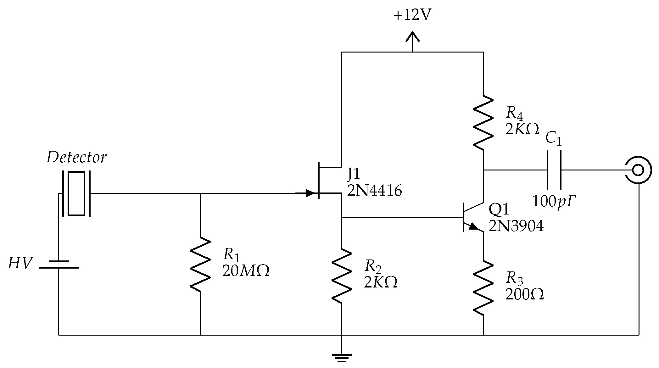
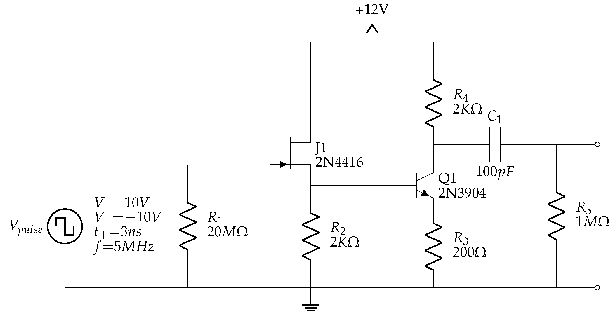
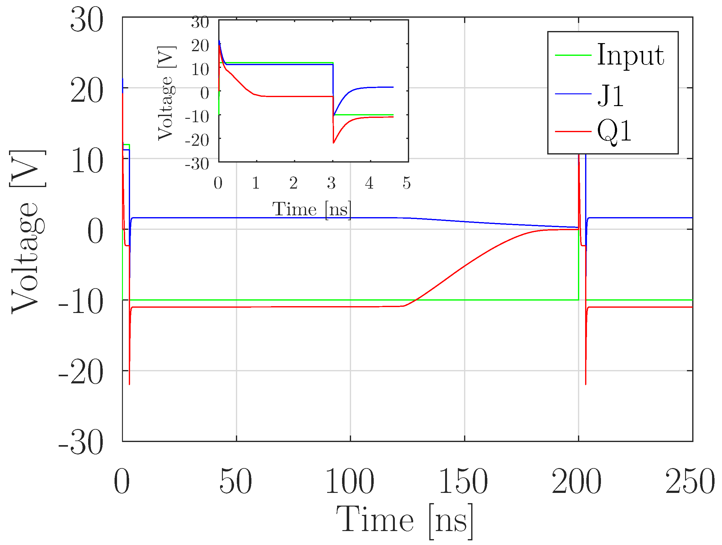
3.1.1. JFET Input and Bipolar Transistor at the Output

Figure 4 displays the simulated circuit of a preamplifier with a JFET at the input (2N4416) and a generic bipolar transistor at the output (2N3904). The input stage consists of a high-impedance source follower further amplified by the generic transistor.
Instead of the detector, we inserted a pulse generator with a pulse height of 20 V, a pulse width of 3 ns, and a period of 200 ns. Figure 5 displays the simulation results of the pulse at the output of the JFET (J1) and the generic transistor (Q1).
From the simulation, it is obvious that the reverse recovery charge Q r r of the JFET and the resulting current I r r lead to spikes in the drain-source voltage. It can be seen that while the JFET response tracks the pulse fairly well, a residual voltage at the output results in Q1 conducting, increasing the response time of the circuit to approximately 200 ns. In the inset, the response of both transistor outputs at the duration of the pulse is shown.

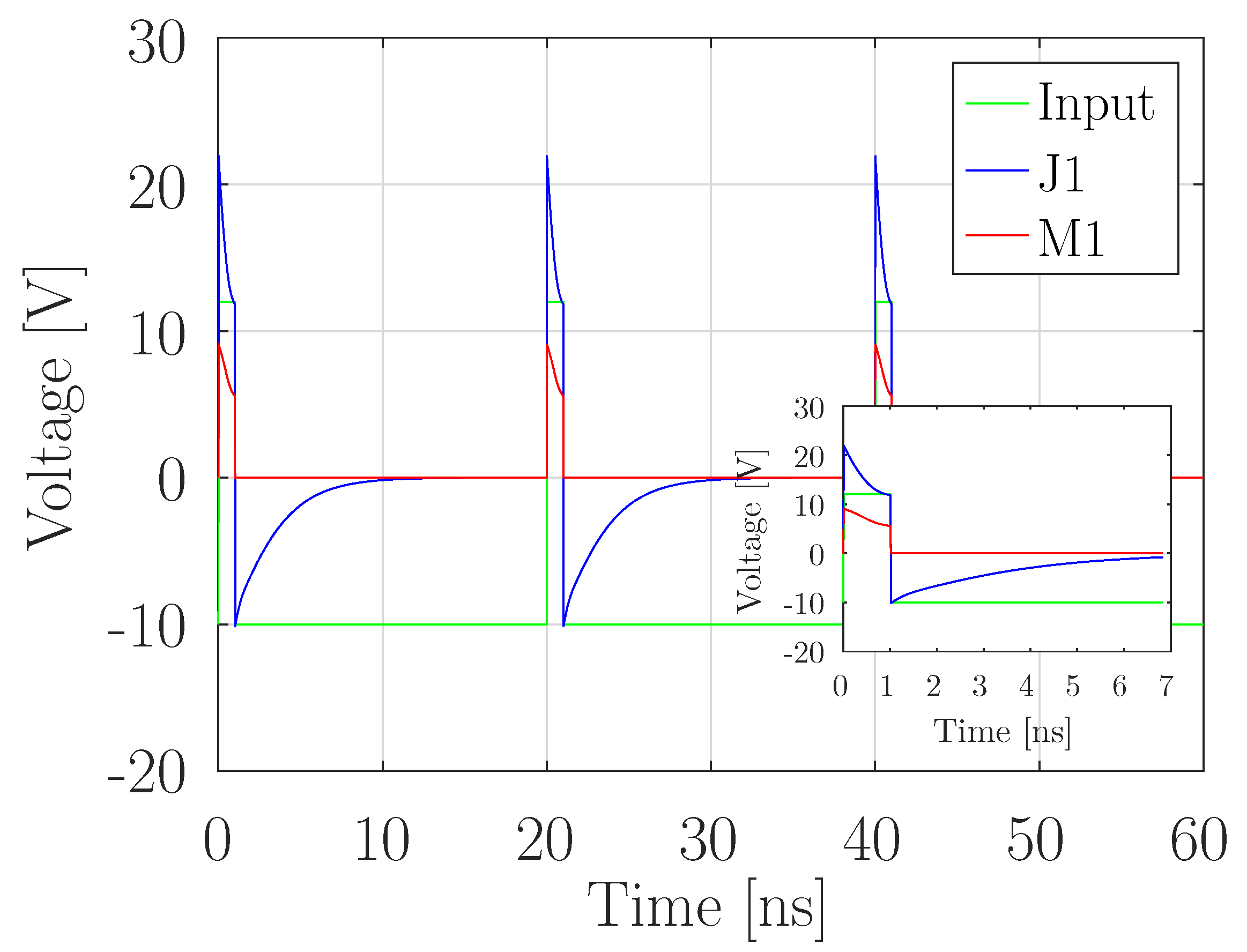
3.1.2. JFET Input and NMOS Output

At this stage, we tested whether an improvement was achieved using an NMOS at the output. Figure 6 illustrates the circuit used to simulate the preamplifier with the same JFET at the input but with a generic enhanced NMOS transistor at the output (2N7000). As the output consists of a source follower, we do not expect a shift in the output.
Once again, the circuit’s response was tested with a periodic short pulse, but as this circuit has a faster response, the pulse width was reduced to 1 ns with a period of 20 ns. Figure 7 displays the resulting simulated signals at the output of the JFET (J1) and the NMOS FET (M1).
In this instance, it is seen that the small-signal NMOS FET does not display the negative voltage-induced reverse recovery charge behavior while maintaining the width of the input pulse, though it does not completely track its form. It can be seen from Figure 7 that this has mostly to do with the JFET at the input.

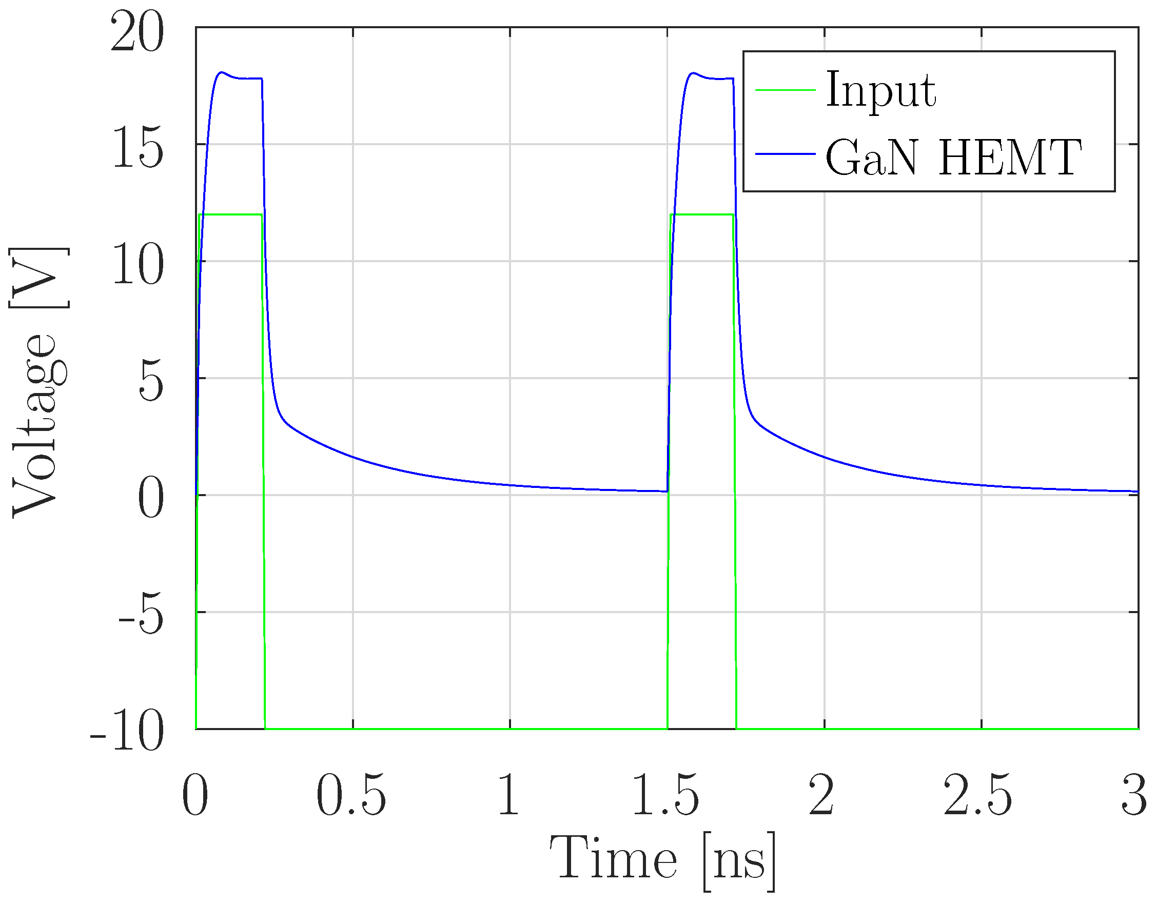
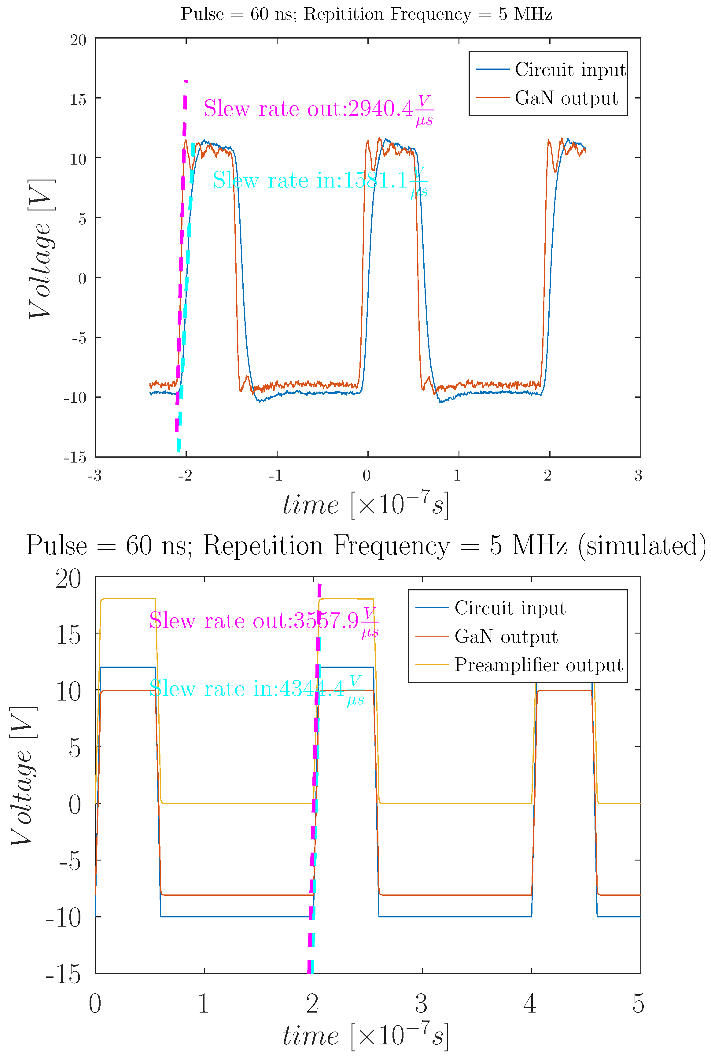
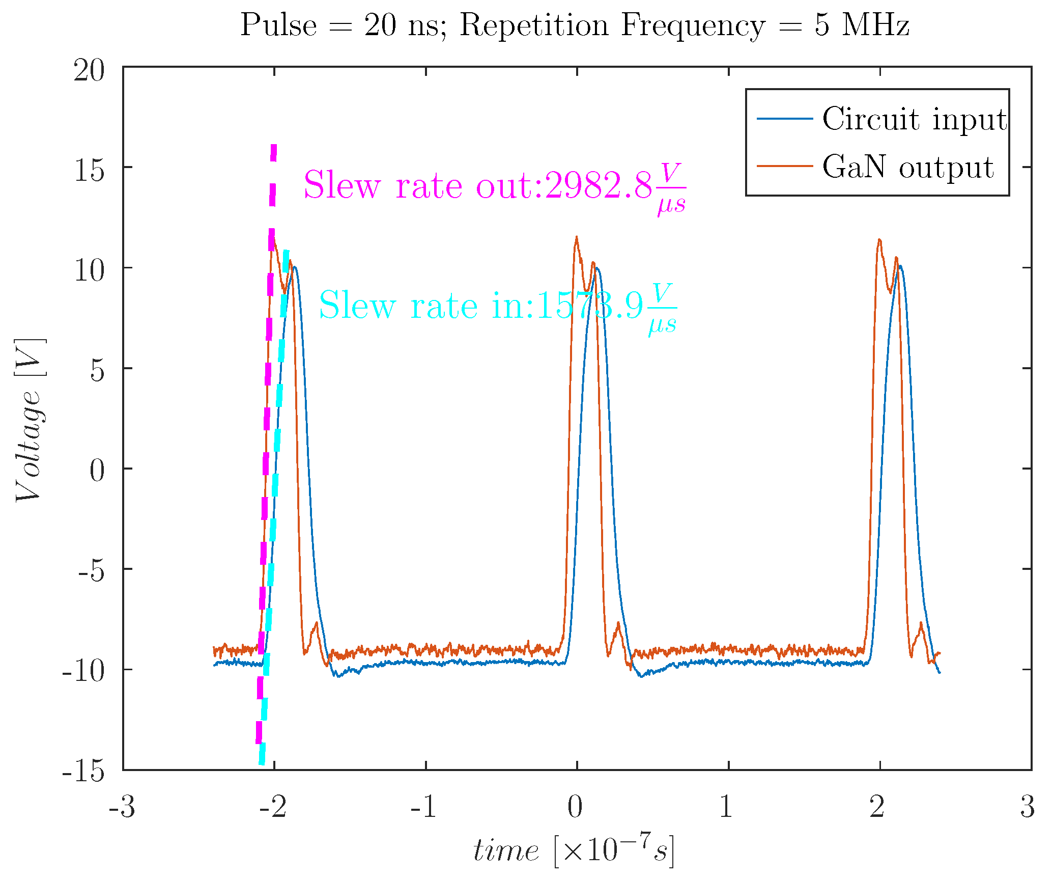
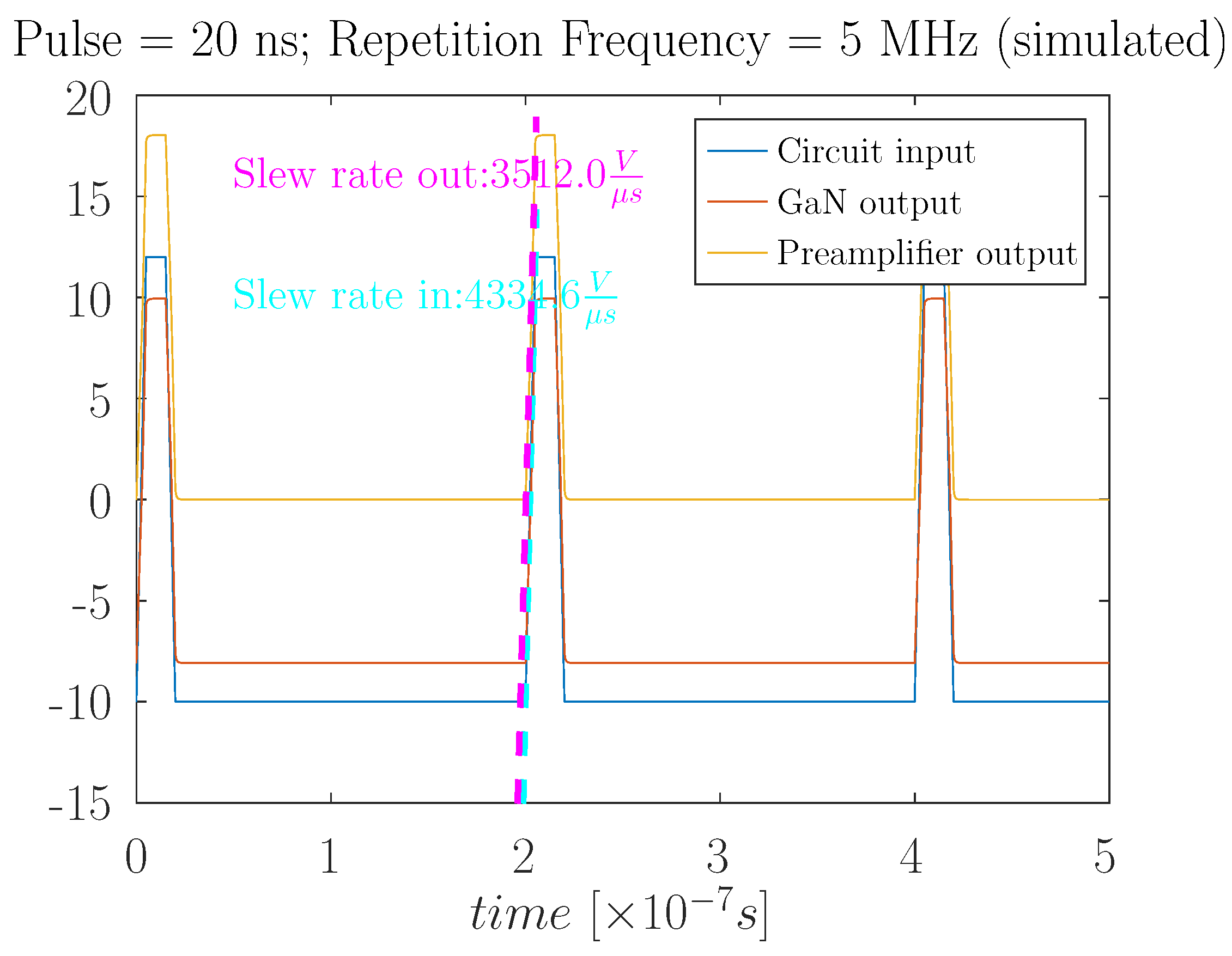
3.1.3. GaN HEMT Preamplifier

Figure 8 displays a preamplifier circuit based on a GaN transistor (EPC2038). The transistor is wired as a source follower.
This circuit is expected to display a faster response. The test signal consists of a 200 ps wide pulse with a 1.5 ns period. Figure 9 displays the resulting signals at the output of the GaN HEMT (U1) and the NMOS FET (M1).
The simulation of this configuration shows a much better response, tracking the input signal with an acceptable fidelity at the output.

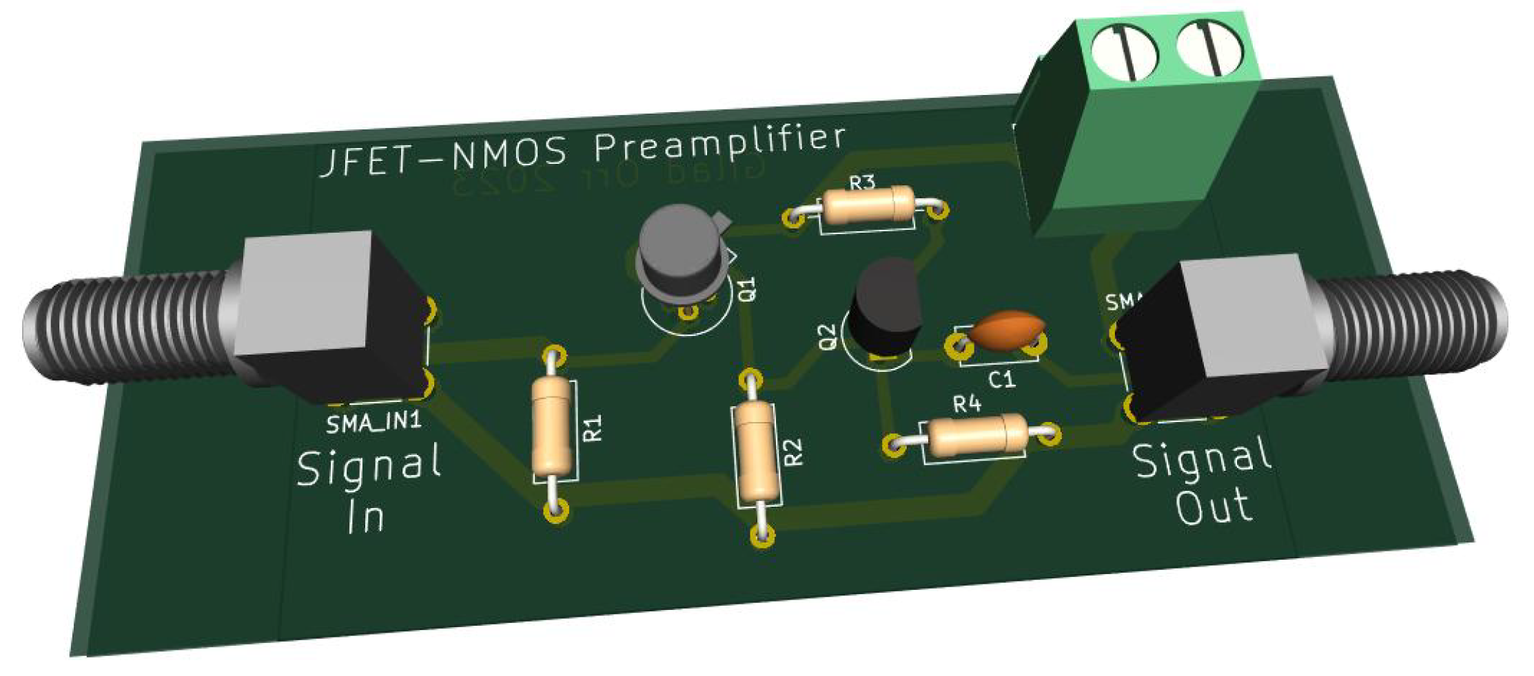
3.2. Practical Amplifier Circuits

Once we acquired some understanding of the preamplifier circuit feasibility and expected response, we proceeded to realize them as physical circuits. The circuits were an exact implementation of the simulated circuits. An Agilent 33250 80 MHz Function/Arbitrary waveform generator, which can go all the way down to an 8 ns pulse, was used as a test input signal for the various amplifiers. It was set to a 5 MHz repetition rate with 8, 10, 12, 15, 20, 25, 30, 40 and 60 ns pulse widths. The pulse amplitude was 20 V, rising from −10 V to 10 V. The generator features a minimum pulse width of 8 ns and a minimum rise time of 5 ns. Sampling was conducted using a Rohde Schartz RTM3004, 10 Bit, 5 GSa/s with a 1 GHz bandwidth. RT-ZP05, 10:1 ratio probes with a 500 MHz bandwidth, an impedance of 10 MΩ/10 pF, and a typical rise time of 0.7 ns were used. Four points were sampled, namely at the input, at the output of the first amplifying stage, at the output of the second amplifying stage (with the DC bias), and at the preamplifier output beyond the 100 pF output capacitor. The following graphs for the various circuits illustrate their response to the generator pulse, given its minimum pulse width and rise time. The response of the physical circuit is compared to the simulated response, cross-validating both the circuits and the simulation.

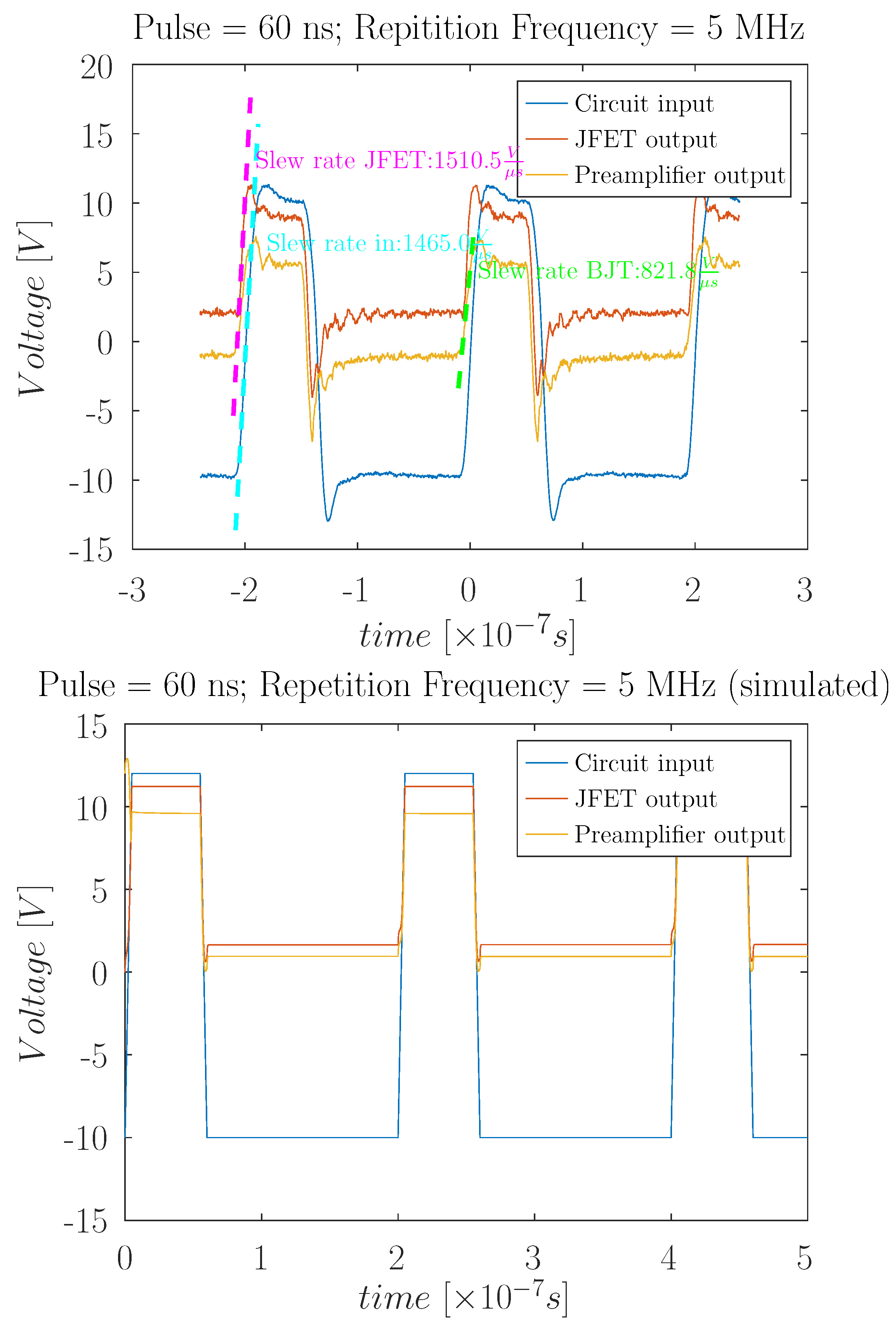
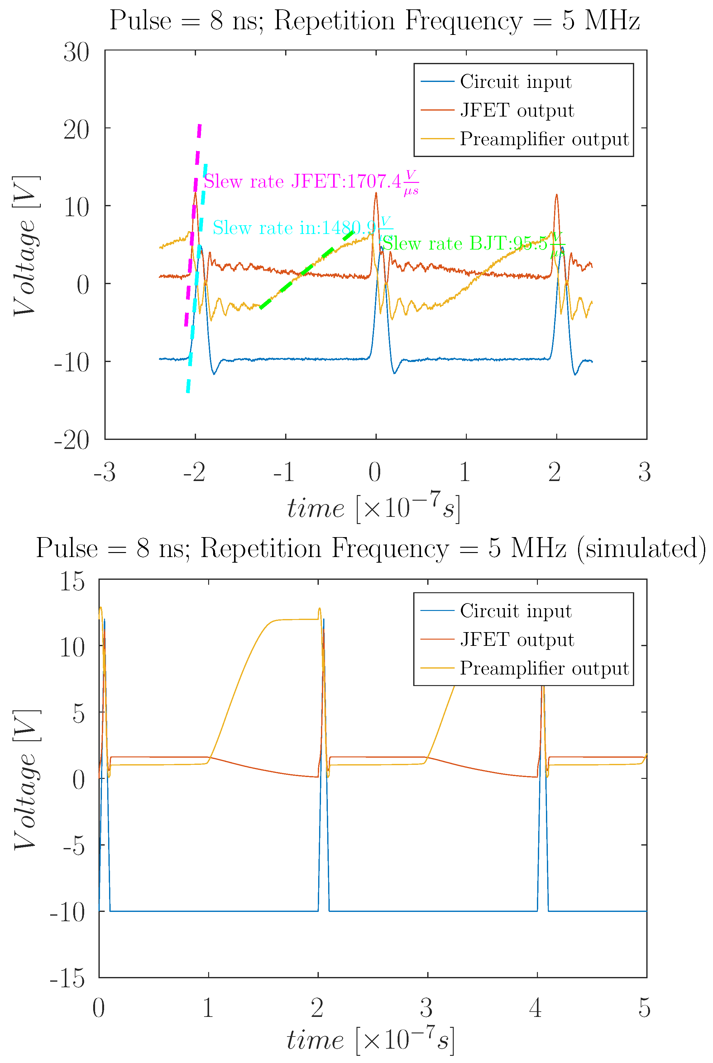
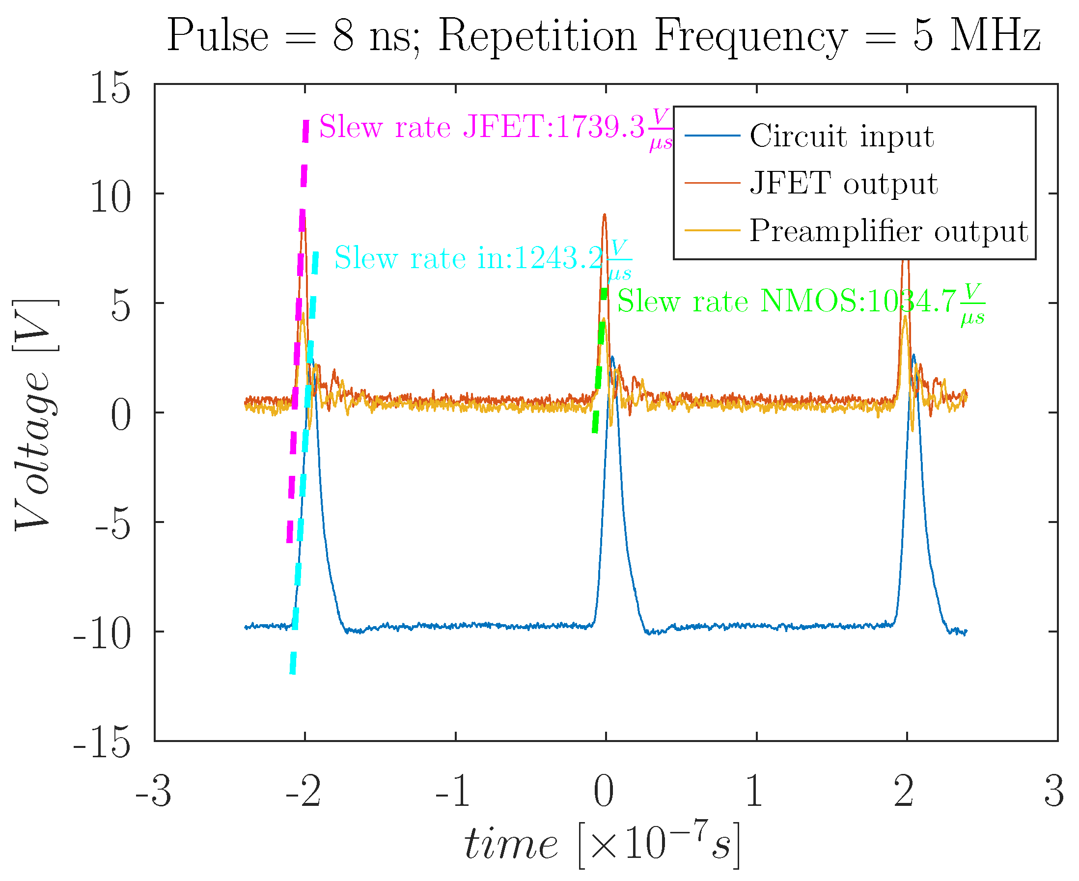
3.2.1. JFET Input with a Bipolar Transistor at the Output

We begin by demonstrating measurements regarding the circuit with the JFET at its input stage (Figure 4). At the second stage, we used a standard general 2N3904 NPN transistor. At the input stage, we used a mil-spec 2N4416 N-Channel JFET in a TO206AF hermetically sealed package. Figure 10, Figure 11 and Figure 12 illustrate the measured response of the preamplifier to a repetitive 5 MHz pattern pulses of 60, 24, and 8 ns.
The reason for displaying the simulated and measured results at the different pulse widths is to conduct a comparative study of the different circuits that have different response times. Hence, displaying the 60 ns pulse width response in the faster circuits is essential.
In all the circuits, the fast rise time and tracking of the JFET at the first stage is evident. Compared to the 5 ns rise time of the pulse generator, its response is almost instantaneous. This does not apply to the general type of transistor, which is evident from the response to the 8 ns input in both the physical implementation of the circuit and the simulation. We can observe in the figures of the described setup that the measured circuit rise time is much faster than the rise time of the generator pulse. As the JFET gate voltage starts opening the channel at approximately −8 V, the voltage across R 2 rises much faster than the rise of the pulse of the generator. This fast rise produces the perception that the output leads the input. In fact, it is the input signal that triggers the extremely fast response at the transistor output across R 2 during the very early stages of the generator pulse rise.

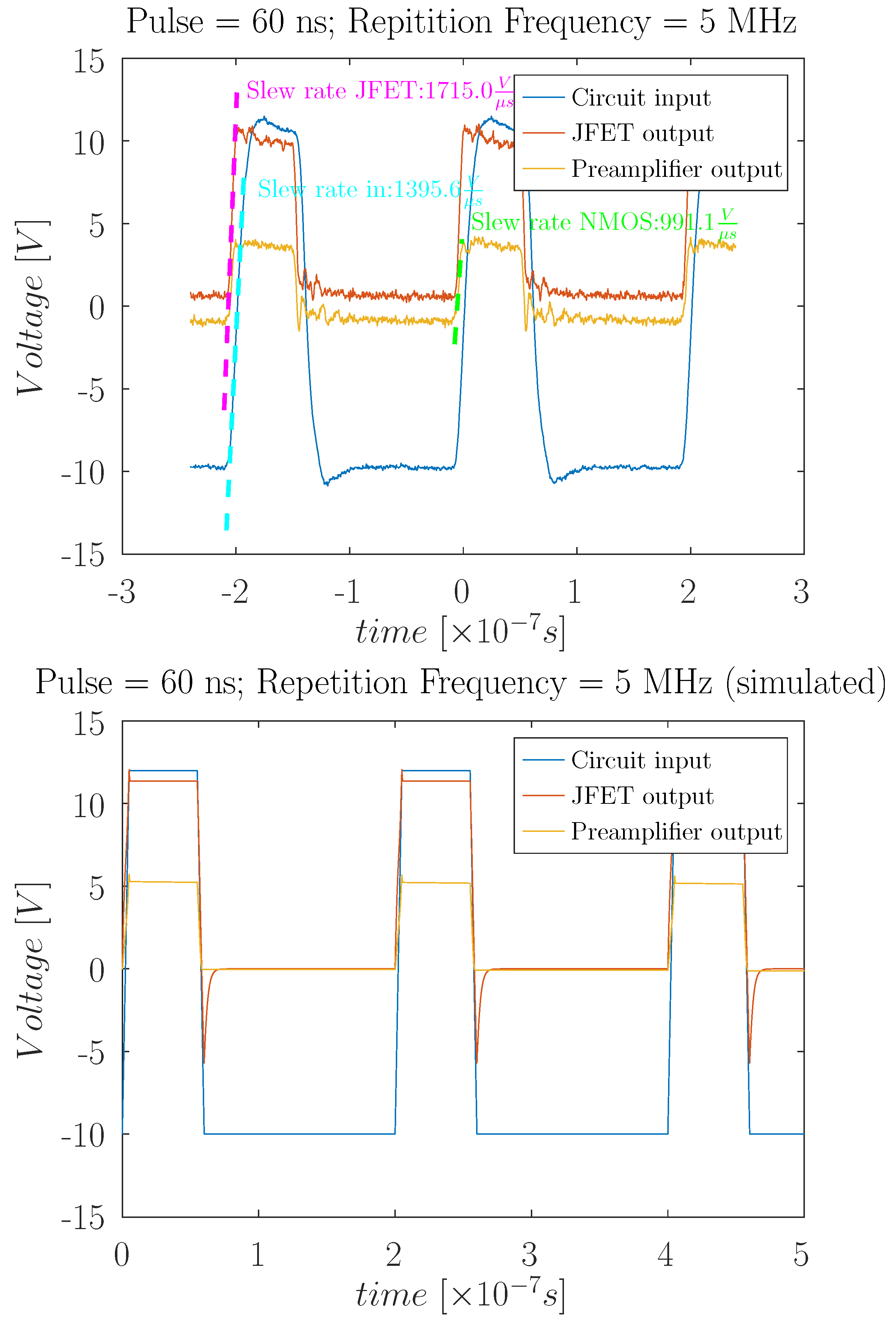
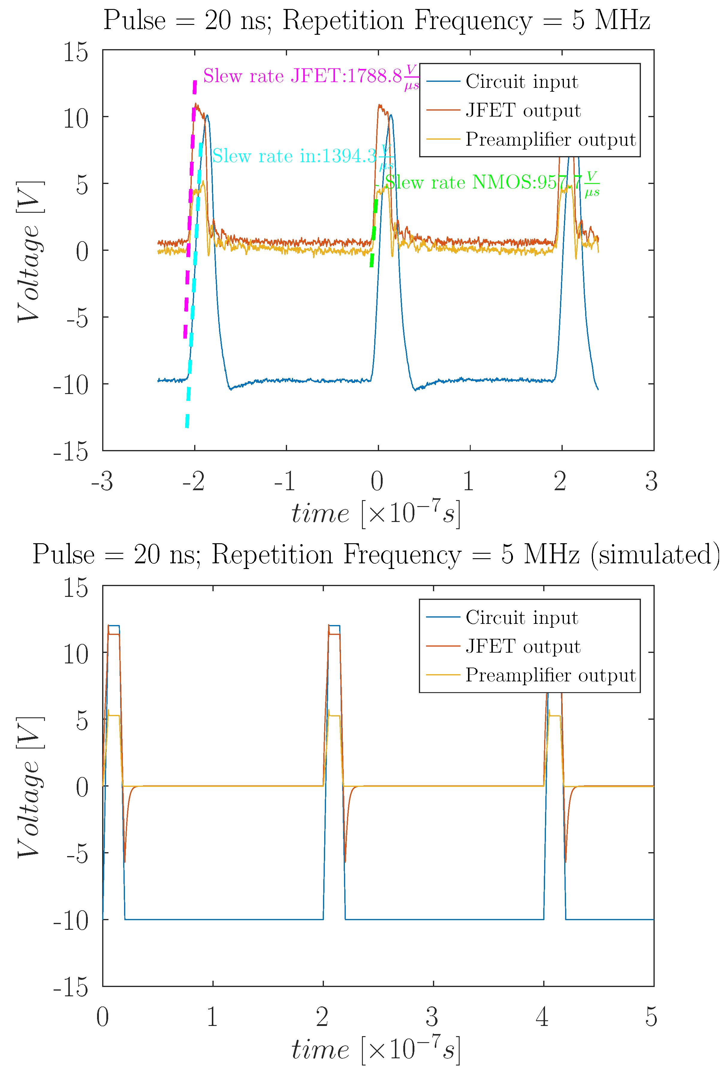
3.2.2. JFET Input and NMOS Output

Next, we test the 2N4416 JFET at the input with a standard 2N7000 NMOS at the output. Figure 13, Figure 14 and Figure 15 illustrate the measured response of the preamplifier to a repetitive 5 MHz pulses of 60, 20, and 8 ns.
Once again, the time response of the circuit regarding the pulse is fast, displaying a faster response than the 5 ns rise time of the generator. In this instance, the NMOS output tracks the JFET output without a noticeable delay at any of the pulse widths. This behavior is predicted by the simulation, deviating only on the account that the physical JFET does not display an overshoot when switched off. It can indicate that the actual JFET has either a much higher resistance or a lower capacitance than the parameters given in the simulation.

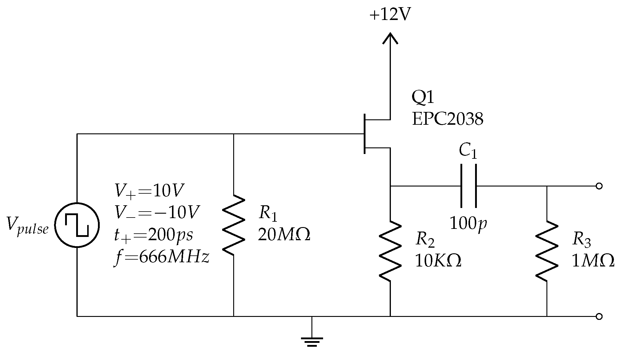
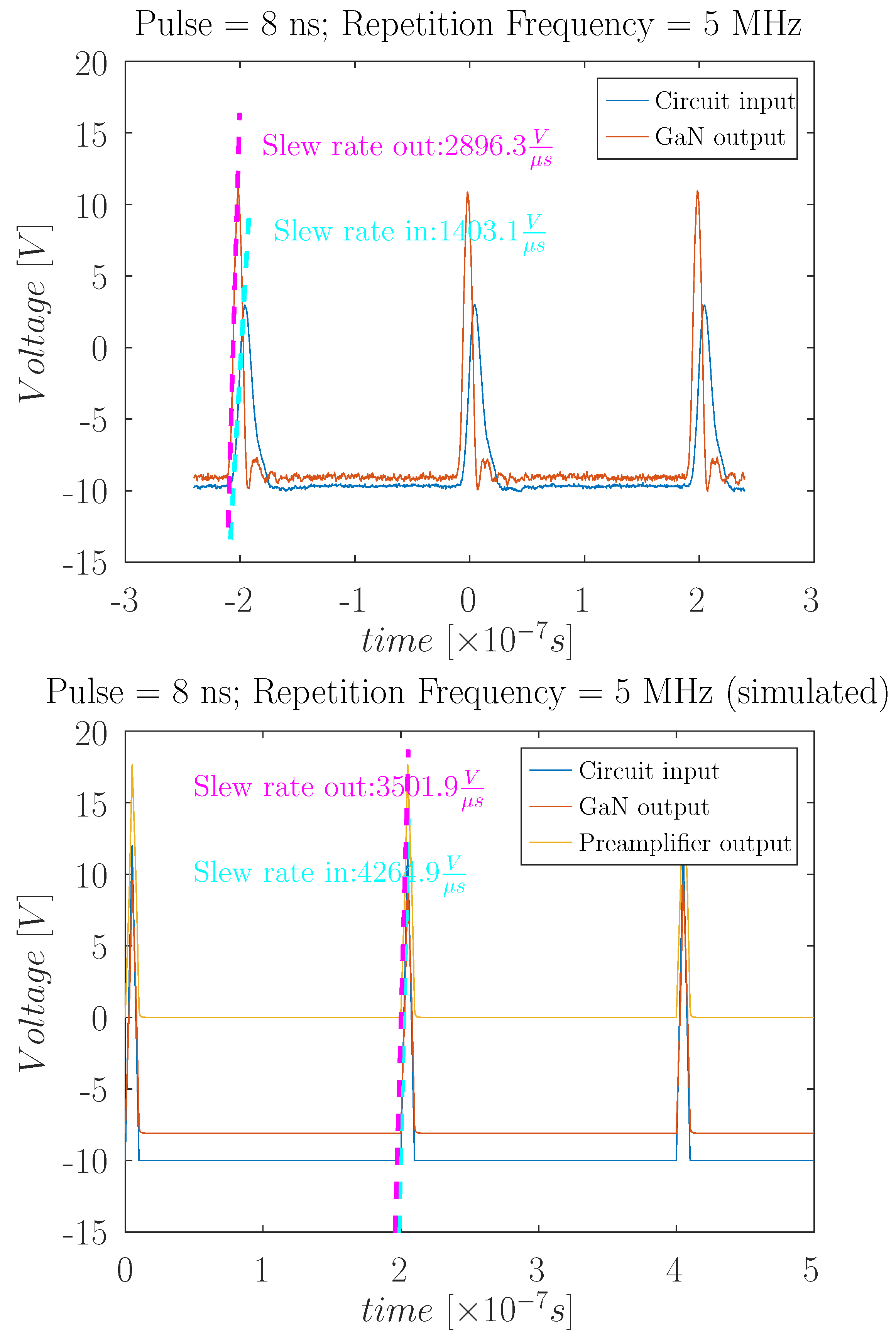
3.2.3. GaN HEMT Single Stage

This work lays the basis for the GaN HEMT as a hardened transistor in a preamplifier circuit. Therefore, we tested it in a single-stage configuration. In many circumstances, this may suffice, providing, as we shall see, a much faster response time with high sensitivity. The circuit was realized using an EPC2038 GaN HEMT. The response of the single-stage GaN preamplifier is illustrated in Figure 16, Figure 17 and Figure 18. As the sensitivity of the GaN to the input is very strong, we compared the rate of change of the voltage at the input and output, as it is obvious from the measured results that it is much faster at the output. We will refer to this rate of voltage change (maybe in an unorthodox manner) as the slew rate. In order to avoid cluttering the graphs and keeping them clear, we opted to omit the output at the preamplifier (after the capacitor) and display only the measured output at the GaN transistor. The behavior at the output of the preamplifier is similar to the behavior shown in the simulation.
From Figure 16, Figure 17 and Figure 18, it is obvious that in the real world, the GaN’s slew rate is higher than the slew rate of the generator that we used. According to the displayed figures, one can see that the GaN’s slew rate at ∼3000 V/μs is approximately double that of the source at ∼1500 V/μs. On the other hand, looking at the response simulation, we may say that the model approximates the GaN’s behavior with a slew rate of ∼3500 V/μs. The frequency generator has less than half the specified slew rate of ∼4300 V/μs; thus, in the experimental results, it seems to lag behind the transistors.

3.2.4. Result Summary

Figure 10, Figure 11, Figure 12, Figure 13, Figure 14, Figure 15, Figure 16, Figure 17 and Figure 18 demonstrate the behavior of the different transistors, with the most significant characteristic they display being the response to pulses of varying widths. We can compare the different transistors using their slew rate for a given pulse width. Table 3 compares the slew rate of the different transistors in the above actual preamplifiers based on the displayed results in the above figures.
The table demonstrates that using a BJT for the second stage of the amplifier (due to its current draw, it cannot be placed in the first stage) loads the JFET and affects its response, reducing its slew rate. It is interesting to note that for a very short pulse (8 ns), the BJT is too slow to respond and effectively does not load the JFET. Hence, it displays its maximum slew rate. It is obvious that this circuit (Figure 4) cannot amplify short pulses, and the second stage, if not harmful, is redundant. The JFET/NMOS combination (Figure 6) shows a fairly consistent behavior given the different pulse widths, providing a slew rate of approximately 1700 V / μ s at the JFET output and approximately 1000 V / μ s at the NMOS output. Thus, the second stage reduces the response of the circuit. Finally, the GaN preamplifier (Figure 6) shows a consistent slew rate of nearly double when compared to the output of a JFET or triple when compared to the NMOS. On this one account, the GaN HEMT is superior to silicon base transistors, but as we have seen, this is only part of its improved characteristics. A second important property is that due to the material’s large bandgap, the GaN HEMT is inherently radiation-hardened. This lends itself to attaching the transistor to the detector, thus reducing input impedance and increasing the system response and SNR when compared to silicon-based devices, which must be shielded and distanced from the detector. This adds to circuit complexity and bulkiness and increases circuit impedance, resulting in lower response and SNR.

4. Discussion

Having a wide bandgap of 3.44 eV, a critical field strength of 6 × 10 6 V/cm and high electron mobility of 2000 cm2/V · s positions the GaN HEMT as a very promising material for fast and hardened transistors required for radiation detectors. Further increasing its frequency performance is the creation of a layered structure resulting in a high-electron-mobility transistor (HEMT). Such transistors are now commercially available on both silicon and silicon carbide substrates, mostly oriented to fast-switching power applications. Our application is somewhat different, as we intend to use the transistors for amplifying small signals in an environment with high-energy particles and radiation, for which we need a radiation-hardened and wide-bandwidth preamplifier responding to short events, thus increasing our time resolution. The response of several preamplifier circuits was examined by both simulation and practical circuits. The first was a simple two-stage amplifier with a wide-bandwidth silicon JFET at the input and a bipolar transistor at the output. This was followed by a circuit consisting of a JFET at the input and an NMOS FET at the output. In the following simulation, the input transistor was replaced by a GaN HEMT, which is commercially available. The simulation results illustrate the superior performance of the GaN HEMT, reliably amplifying pulses without much distortion down to pulse widths of 200 ps. As a whole, we see the response of the physical circuits agreeing well with the simulations. Both the JFET input circuits and the GaN preamplifier display a fast response to the input displaying a much faster slew rate compared to the input signal. It was found that the actual slew rate of the GaN was approximately 3000 V / μ s , which is 17 % lower than what is predicted by the simulation. To our knowledge, no such comparative study has previously been published.
This experimental work consists of some of the required underlying work for the fabrication of fast and hardened preamplifiers for the next generation of γ detection materials such as C s P b B r 3 which can be fabricated into self-healing low noise γ detection and imaging devices [5,26]. It shows promise for designing improved long MTBF imaging circuits required by next-generation industrial-process gamma transmission-computed tomography.

Author Contributions

Conceptualization, G.O.; methodology, G.O.; validation, A.B., G.G., and M.A.; analysis G.O. and M.A.; investigation, G.O. and M.A.; resources, G.O. and M.A.; data curation, G.O.; writing—original draft preparation, G.O.; writing—review and editing, G.O., G.G., and A.B.; visualization, G.O. and M.A. All authors have read and agreed to the published version of the manuscript.

Funding

This research received no external funding.

Institutional Review Board Statement

Not applicable.

Informed Consent Statement

Not applicable.

Data Availability Statement

Contact the corresponding author for more information.

Conflicts of Interest

The authors declare no conflicts of interest.

References

  1. Busch, M.; Hausotte, T. Practical Approaches for Determining the Structural Resolution Capability of X-ray Computed Tomography Measurement Tasks. Metrology 2024, 4, 457–468. [Google Scholar] [CrossRef]
  2. De Andrade, V.; Nikitin, V.; Wojcik, M.; Deriy, A.; Bean, S.; Shu, D.; Mooney, T.; Peterson, K.; Kc, P.; Li, K.; et al. Fast X-ray Nanotomography with Sub-10 nm Resolution as a Powerful Imaging Tool for Nanotechnology and Energy Storage Applications. Adv. Mater. 2021, 33, 2008653. [Google Scholar] [CrossRef] [PubMed]
  3. Matsuyama, S.; Nakamori, H.; Goto, T.; Kimura, T.; Khakurel, K.P.; Kohmura, Y.; Sano, Y.; Yabashi, M.; Ishikawa, T.; Nishino, Y.; et al. Nearly diffraction-limited X-ray focusing with variable-numerical-aperture focusing optical system based on four deformable mirrors. Sci. Rep. 2016, 6, 24801. [Google Scholar] [CrossRef] [PubMed]
  4. Grunwaldt, J.D.; Schroer, C.G. Hard and soft X-ray microscopy and tomography in catalysis: Bridging the different time and length scales. Chem. Soc. Rev. 2010, 39, 4741–4753. [Google Scholar] [CrossRef] [PubMed]
  5. Hawrami, R.; Matei, L.; Ariesanti, E.; Buliga, V.; Parkhe, H.; Burger, A.; Stewart, J.; Piro, A.; De Figueiredo, F.; Kargar, A.; et al. Growth and Performance of Perovskite Semiconductor CsPbX3 (X= Cl, Br, I, or Mixed Halide) for Detection and Imaging Applications. Materials 2024, 17, 5360. [Google Scholar] [CrossRef] [PubMed]
  6. Wellmann, P.J. Power electronic semiconductor materials for automotive and energy saving applications–SiC, GaN, Ga2O3, and diamond. Z. Fur Anorg. Und Allg. Chem. 2017, 643, 1312–1322. [Google Scholar] [CrossRef] [PubMed]
  7. Microsemi, P. Gallium nitride (GaN) versus silicon carbide (SiC) In the High Frequency (RF) and power switching applications. Digi-key 2014, 82, 2014. [Google Scholar]
  8. Ren, F.; Zolper, J.C. Wide Energy Bandgap Electronic Devices; World Scientific: Singapore, 2003. [Google Scholar]
  9. Ayzenshtat, G.; Bozhkov, V.; Yushchenko, A.Y. Measurement of the electron saturation velocity in an AlGaAs/InGaAs quantum well. Russ. Phys. J. 2011, 53, 914–920. [Google Scholar]
  10. Pierron, E.D.; Parker, D.L.; McNeely, J.B. Coefficient of Expansion of GaAs, GaP, and Ga(As, P) Compounds from −62 °C to 200 °C. J. Appl. Phys. 1967, 38, 4669–4671. [Google Scholar] [CrossRef]
  11. Guo, B.; Yu, G.; Zhang, L.; Zhou, J.; Wang, Z.; Xing, R.; Yang, A.; Li, Y.; Liu, B.; Zeng, X.; et al. High-Performance N-Polar GaN/AlGaN Metal–Insulator–Semiconductor High-Electron-Mobility Transistors with Low Surface Roughness Enabled by Chemical–Mechanical-Polishing-Incorporated Layer Transfer Technology. Crystals 2024, 14, 253. [Google Scholar] [CrossRef]
  12. Meneghini, M.; Hilt, O.; Wuerfl, J.; Meneghesso, G. Technology and Reliability of Normally-Off GaN HEMTs with p-Type Gate. Energies 2017, 10, 153. [Google Scholar] [CrossRef]
  13. Haziq, M.; Falina, S.; Manaf, A.A.; Kawarada, H.; Syamsul, M. Challenges and Opportunities for High-Power and High-Frequency AlGaN/GaN High-Electron-Mobility Transistor (HEMT) Applications: A Review. Micromachines 2022, 13, 2133. [Google Scholar] [CrossRef] [PubMed]
  14. Pengelly, R.S.; Wood, S.M.; Milligan, J.W.; Sheppard, S.T.; Pribble, W.L. A review of GaN on SiC high electron-mobility power transistors and MMICs. IEEE Trans. Microw. Theory Tech. 2012, 60, 1764–1783. [Google Scholar] [CrossRef]
  15. Harris, C.; Pengelly, R.; Sheppard, S.; Smith, T.; Pribble, B.; Wood, S.; Platis, C. Commercial gan devices for switching and low noise applications. In Proceedings of the CS MANTECH Conference, Palm Springs, CA, USA, 16–19 May 2011. [Google Scholar]
  16. Kabouche, R.; Pecheux, R.; Harrouche, K.; Okada, E.; Medjdoub, F.; Derluyn, J.; Degroote, S.; Germain, M.; Gucmann, F.; Middleton, C.; et al. High efficiency AlN/GaN HEMTs for Q-band applications with an improved thermal dissipation. Int. J. High Speed Electron. Syst. 2019, 28, 1940003. [Google Scholar]
  17. Li, L.; Nomoto, K.; Pan, M.; Li, W.; Hickman, A.; Miller, J.; Lee, K.; Hu, Z.; Bader, S.J.; Lee, S.M.; et al. GaN HEMTs on Si with regrown contacts and cutoff/maximum oscillation frequencies of 250/204 GHz. IEEE Electron Device Lett. 2020, 41, 689–692. [Google Scholar] [CrossRef]
  18. Kim, H.S.; Kang, M.J.; Kim, J.J.; Seo, K.S.; Cha, H.Y. Effects of Recessed-Gate Structure on AlGaN/GaN-on-SiC MIS-HEMTs with Thin AlOxNy MIS Gate. Materials 2020, 13, 1538. [Google Scholar] [CrossRef] [PubMed]
  19. Kumar, A.; Gupta, N.; Goyal, A.K.; Massoud, Y. Comprehensive power gain assessment of GaN-SOI-FinFET for improved RF/wireless performance using TCAD. Micromachines 2022, 13, 1418. [Google Scholar] [CrossRef] [PubMed]
  20. Vishay. 2N4416-N-Channel JFETs. 2025. Available online: https://mm.digikey.com/Volume0/opasdata/d220001/medias/docus/412/2N4416%2C2N4416A.SST4416.pdf (accessed on 2 March 2025).
  21. onsemi. 2N3904-General Purpose Transistors. 2025. Available online: https://www.onsemi.com/download/data-sheet/pdf/2n3903-d.pdf (accessed on 2 March 2025).
  22. onsemi. 2N7000-Small Signal MOSFETs. 2025. Available online: https://www.onsemi.com/products/discrete-power-modules/mosfets/small-signal-mosfets/2n7000 (accessed on 2 March 2025).
  23. Efficient Power Conversion. EPC2038-Enhancement Mode Power Transistor. 2025. Available online: https://epc-co.com/epc/products/gan-fets-and-ics/epc2038 (accessed on 2 March 2025).
  24. TDK. CC45 Series-High Voltage Ceramic Capacitors, Commercial Grade, Low Dissipation at High Frequency. 2025. Available online: https://product.tdk.com/system/files/dam/doc/product/capacitor/ceramic/lead-disc/catalog/leaddisc_commercial_cc45_en.pdf (accessed on 2 March 2025).
  25. Zuck, A.; Schieber, M.; Khakhan, O.; Gilboa, H.; Burshtein, Z. Microstructure and energy resolution of 59.6 keV 241Am gamma absorption in polycrystalline HgI2 detectors. IEEE Trans. Nucl. Sci. 2004, 51, 1250–1255. [Google Scholar]
  26. Orr, G.; Matei, L.; Zuck, A.; Zinigrad, M.; Ariesanti, E.; Hawrami, R.; Burger, A. Cesium Lead Bromide Crystal Growth: An investigation guided by lessons learned from the family of heavy metal compounds for radiation detection. In Proceedings of the Semiconductors Session at the ICCGE Conference, Naples, Italy, 30 July–4 August 2023. [Google Scholar]
Figure 1. Basic GaN/AlGaN HEMT.
Metrology 05 00021 g001
Figure 2. Component layout of the preamplifier with a JFET at its input stage and an NMOS at its output stage. The other test boards have a similar layout.
Metrology 05 00021 g002
Figure 3. Simple preamplifier using a JFET transistor in its first stage.
Metrology 05 00021 g003
Figure 4. A preamplifier detection simulation circuit with a JFET at the first stage and a generic bipolar transistor at the second stage.
Metrology 05 00021 g004
Figure 5. Response simulation of the circuit with a JFET at its input and a generic transistor at its output.
Metrology 05 00021 g005
Figure 6. A preamplifier-detection simulation circuit with a JFET at the first stage and a generic enhanced NMOS FET at the output stage.
Metrology 05 00021 g006
Figure 7. Response simulation of the circuit with a JFET at its input and NMOS FET at its output.
Metrology 05 00021 g007
Figure 8. A GaN HEMT-based two-stage preamplifier with a GaN HEMT transistor at the input and an NMOS FET at the output.
Metrology 05 00021 g008
Figure 9. Response simulation of the circuit with a GaN HEMT at its input and NMOS FET at its output.
Metrology 05 00021 g009
Figure 10. JFET-Bipolar transistor preamplifier response to 60 ns pulses. The bottom figure is the response simulation, while the top figure is the measured results.
Metrology 05 00021 g010
Figure 11. JFET-Bipolar transistor preamplifier response to 20 ns pulses. The bottom figure is the sethlcolorgreenhlresponse simulation, while the top figure is the measured results.
Metrology 05 00021 g011aMetrology 05 00021 g011b
Figure 12. JFET-Bipolar transistor preamplifier response to 8 ns pulses. The bottom figure is the response simulation, while the top figure is the measured results.
Metrology 05 00021 g012
Figure 13. JFET-NMOS transistor preamplifier response to 60 ns pulses. The bottom figure is the response simulation, while the top figure is the measured results.
Metrology 05 00021 g013
Figure 14. JFET-NMOS transistor preamplifier response to 20 ns pulses. The bottom figure is the response simulation, while the top figure is the measured results.
Metrology 05 00021 g014
Figure 15. JFET-NMOS transistor preamplifier response to 8 ns pulses. The bottom figure is the response simulation, while the top figure is the measured results.
Metrology 05 00021 g015aMetrology 05 00021 g015b
Figure 16. GaN transistor preamplifier response to 60 ns pulses. The bottom figure is the response simulation, while the top figure is the measured results.
Metrology 05 00021 g016
Figure 17. GaN transistor preamplifier response to 20 ns pulses. The bottom figure is the response simulation, while the top figure is the measured results.
Metrology 05 00021 g017aMetrology 05 00021 g017b
Figure 18. GaN transistor preamplifier response to 8 ns pulses. The bottom figure is the response simulation, while the top figure is the measured results.
Metrology 05 00021 g018
Table 1. Electrical and physical properties of wide-bandgap semiconductors.
Property SiGaAsSiCGaN
Band gap E G [eV] [6]1.11.422.3~3.33.44
Critical field strength E C [ 10 6 V/cm] [6]0.40.546
Mobility μ [ cm 2 / V · s ] [7,8]145050009002000
Thermal conductivity κ [ W / cm · K ] [6]1.50.53~51.3
Electron saturation velocity v e s a t 10 7 cm / s [7,8,9]11.42.23
Lattice Constant ( Å ) [6,7]5.435.653.083.19
Coefficient of Thermal Expansion α [ 10 6 × K 1 ] [7,10]2.66.864.25.6
Table 2. Dielectric constant of several common semiconducting materials.
Material ε r [14]
GaAs12.5
InP12.4
Si11.9
SiC10.0
GaN9.5
Diamond5.5
Table 3. Slew rate comparison of the different transistors in the actual amplifiers.
Pulse Width [ns]JFET/BJT [V/μs]JFET/NMOS [V/μs]GaN [V/μs]
601510/8211715/9912940
201453/7981789/9572982
81707/961739/10352896
Disclaimer/Publisher’s Note: The statements, opinions and data contained in all publications are solely those of the individual author(s) and contributor(s) and not of MDPI and/or the editor(s). MDPI and/or the editor(s) disclaim responsibility for any injury to people or property resulting from any ideas, methods, instructions or products referred to in the content.

