1. Introduction
The Earth maintains its habitable temperature through the natural greenhouse effect, which occurs when atmospheric gases trap infrared radiation (IR) released by the planet [
1]. Earth’s IR becomes trapped by gases H
2O, CO
2, CH
4, O
3, and N
2O because these molecules align their vibrations with IR wavelengths [
2,
3]. The intensified greenhouse effect from excessive greenhouse gases (GHGs) results in global warming and climate change.
The increase in CO
2 emissions has been substantial since 1900, with gas levels rising by 90% between 1970 and 2011, primarily due to fossil fuel combustion and industrial activities. In 2018, atmospheric CO
2 represented 82.5% of total GHG emissions, followed by CH
4 at 11.6% and N
2O at 3.0% [
4]. Emissions from China accounted for 30.12% of global CO
2 and 26.03% of total GHGs, while the United States remained the second-largest emitter [
5]. Emission levels increased at 1.6% annually from 1970 to 2003, followed by a sharp 3.2% growth per year from 2003 to 2011, and then decreased to 1.3% per year between 2012 and 2014. The type of fuel used for energy production significantly influences emission patterns.
While solid fuels dominated early industrialization, liquid fuels have become the primary contributor to modern temperature increases. In 2009, CO
2 emissions dropped by −1.4% due to the global financial crisis but rebounded by +5.1% in 2010 [
3]. Fossil fuels remain the dominant source of electricity production, while agricultural activities and deforestation are the second-largest sources of emissions after energy use. Historical data shows that Europe and the United States produced over 90% of CO
2 emissions throughout the 20th century, until rapid industrial growth in Asia, particularly China, led to a significant shift in global emission shares [
6]. From all these statistics, it is evident that the greenhouse effect significantly impacts the world. Similarly, it also affects individual houses, as explained below.
Room-Level Greenhouse Effect (RGHE)
The greenhouse effect, which operates on a planetary scale, creates similar heating effects within enclosed spaces like buildings that receive substantial solar radiation. The indoor temperature rises substantially when sunlight intensity reaches peak daytime levels in buildings with extensive glass windows or facades [
7]. Glass surfaces allow around 75% of shortwave solar radiation to pass through, while interior elements such as walls, floors, and furniture absorb this transmitted energy. The absorbed energy releases as longwave IR, which becomes trapped as heat in buildings [
3].
The heat becomes trapped inside buildings, which leads to temperature increases of 4 °C to 10 °C above outdoor temperatures, especially in poorly ventilated areas with high solar exposure. The effect from solar radiation generates more than 20% of summer indoor heat gain in buildings when solar radiation maintains its intensity [
3]. As shown in the
Table 1, the RGHE leads to increased cooling energy needs between 15% and 30% in residential and commercial buildings that experience more than 5.5 kWh/m
2 of daily solar exposure [
8]. Real-time sunlight intensity monitoring has become essential because it enables effective management of RGHE consequences in contemporary energy-efficient buildings.
A compact analog microsystem is proposed to monitor the sunlight intensity radiation factor (SIR), denoted as
f (
r), and detect RGHE conditions in real time. The microsystem employs a calibrated analog light sensor whose output voltage varies proportionally with the intensity of incident solar radiation [
8]. The analog signal is processed through a special sensing amplifier circuit designed to amplify only the small AC ripple component corresponding to
f (
r), while actively rejecting the DC component resulting from static room condition factors (RCFs) [
9].
The RCF signal consists of material-dependent parameters such as the number of windows
f (
w), drape transparency
f (
t), wall reflectivity, and other structural attributes. These static environmental characteristics introduce a baseline voltage offset that differs across rooms. For accurate RGHE detection, isolating the time-varying sunlight component
f (
r) from these static influences is essential. The combined RCF signal
f (
m) is modeled as
Here,
f (
w) increases with the number and size of windows, while
f (
t) increases with the transparency of window drapes. A room with large, clear windows will naturally exhibit a higher RCF than a space with shaded or tinted openings. These values are captured during an auto-calibration phase at system setup, allowing for the microsystem to estimate
GRCF [
8]. A low-pass RC filter in the auto-calibration circuit as shown in the
Figure 1 extracts the static component
f (
m) by allowing only low-frequency or DC signals to pass while attenuating dynamic changes like
f (
r). The capacitor smooths out rapid fluctuations, enabling the system to continuously reference
f (
m) for accurate self-calibration. From the equation below, the DC component reflects room-specific static bias, and the sinusoidal term represents dynamic fluctuations in solar intensity over time. This is formally expressed in system-specific terms such as
In this study, representative RCF DC voltages of 0.75 V, 1.0 V, and 1.5 V were used to simulate low-, medium-, and high-exposure room environments. By rejecting static RCF influences and extracting only the f (r) signal, the proposed system enables accurate, real-time RGHE detection and contributes to energy-efficient smart building applications through localized thermal response.
An inexpensive light sensor has a light-dependent resistor (LDR) that uses cadmium sulfide (CdS) as its material. It is highly sensitive to visible light in the 560–610 nm wavelength range. In darkness, an LDR typically exhibits a resistance greater than 10 MΩ, which decreases to approximately 100 Ω under bright light. Its resistance is inversely proportional to light intensity [
9]. This large resistance variation enables effective light-level measurement using a voltage divider circuit. For example, when an LDR is connected in series with a fixed resistor across a 3.3 V DC supply, the output voltage at the junction can range from nearly 0 V in bright light to almost 3.3 V in complete darkness. This analog voltage variation can be directly interpreted as a proxy for sunlight intensity, capturing both
f (
r) and
f (
m), in the proposed RGHE detection system. The ORP12 CdS LDR, with a peak spectral response around 610 nm, is well suited for indoor solar exposure and window-lit sensing applications [
10]. Although LDRs have a slower response time, ranging from milliseconds to seconds, they remain highly effective in passive RGHE systems due to their wide dynamic range, simplicity, and low cost. Instead of LDRs, photodiodes or phototransistors could also be used due to their faster response time and broader spectral sensitivity. The signal from the sensor is applied to the microsystem to isolate the
f (
r) signal for further analysis, as detailed in the following sections.
2. Design Methodology
The proposed micro-design architecture for RGHE detection is divided into three primary functional stages: the Sensing Circuit Stage (SCS), the Amplification Stage (AS), and the Stabilized Peak Detection Stage (SPDS). As shown in the
Figure 2, the microsystem receives an analog voltage from a calibrated LDR, which serves as the input to the system and encodes both the SIR and the room-specific RCF [
11]. The SCS receives a differential input, where the first terminal is driven by a DC reference representing only
f (
m) (i.e., the static RCF component), and the second terminal receives the full composite signal containing both
f (
r) and
f (
m). The SCS functions as a differential amplifier to cancel out the DC offset from
f (
m) so it can output only the dynamic sunlight intensity component
f (
r), which is vital for real-time RGHE monitoring. The
f (
r) signal typically falls within a range of 3–5 mV peak-to-peak (V
pp).
The AS receives the output from the SCS and increases the magnitude of the isolated
f (
r) signal to a level that is suitable for further processing. A precision peak detection circuit in the final SPDS captures and holds the maximum amplitude of the
f (
r) signal to provide a stabilized representation of peak solar exposure for that interval. The peak value directly corresponds to the highest effective SIR impacting the indoor environment [
8]. To simulate different room environments, the static bias
f (
m) was modeled using three DC reference levels: 0.75 V, 1.0 V, and 1.5 V. The microsystem was tested with three representative AC signal amplitudes for
f (
r), 3 mV
pp, 4 mV
pp, and 5 mV
pp, capturing a range of realistic indoor SIR conditions. This structured three-stage design enables the system to accurately sense, extract, and track RGHE-related light variations in dynamic room environments with minimal interference from RCFs. In further sections, all circuits were designed using Cadence Virtuoso software version IC23.1 and the TSMC 180 nm technology library [
10]. The prototype can be designed using smaller technology nodes, which may reduce chip area and power consumption. However, for academic prototyping and ease of design and testing, the 180 nm node was selected. In future work, we plan to explore more advanced nodes for better integration and lower power in compact applications. All simulations were run in the microsecond range for simulation purposes only. However, in real-life scenarios, changes in sunlight intensity occur over much longer periods.
2.1. Sensing Circuitry Stage (SCS)
The SCS is responsible for isolating the dynamic sunlight intensity signal
f (
r) from the composite voltage output generated by the LDR. This composite input includes both the time-varying SIR component
f (
r) and the static RCF component
f (
m). To separate the two, the SCS utilizes an op-amp configured in differential mode, where one terminal receives a DC reference voltage corresponding to
f (
m) (tested with values of 0.75 V, 1.0 V, and 1.5 V), while the other terminal is fed the composite signal containing both
f (
r) and
f (
m) [
12]. By subtracting the reference input from the composite signal, the amplifier cancels out the DC offset contributed by
f (
m), isolating only the AC signal
f (
r) for amplification. The output from the SCS is therefore a clean representation of sunlight intensity variation, with typical
f (
r) values ranging between 3 and 5 mV
pp depending on solar exposure [
13]. The microcircuit diagram for SCS is shown in
Figure 3a, and the symbolized amplifier circuit with the testing setup is presented in
Figure 3b.
The gain of the amplifier is defined as the ratio between the output signal swing and the input signal swing. In this application, it is also determined by the ratio between the feedback resistor (
Rf) and the input resistor (
Rin) [
14]. To amplify the extracted
f (
r), the SCS employs an inverting amplifier configuration for gain control. The standard voltage gain is expressed as
For the selected resistor values
Rf = 100 kΩ and
Rin = 5 kΩ, this yields a gain of
Av = −20. As shown in
Figure 3b,
Rf and
Rin are arranged accordingly. The internal op-amp design uses PMOS microdevices with 4 µm width and 300 nm channel length, and NMOS microdevices with 3 µm width and 350 nm channel length [
15,
16]. A 400 fF compensation capacitor is included for frequency stability. This setup effectively boosts weak AC signals while rejecting DC bias. An alternative gain expression is derived from node analysis at the inverting input of the op-amp:
Thus, the gain
Av can also be expressed as
As shown in the waveform outputs in
Figure 4, all waveforms are plotted with time axis in microseconds (µs). At an input containing 1.5 V DC and a 3 mV AC ripple (red colored signal), the SCS outputs (green colored signal) approximately 45.63 mV. At 1.0 V DC with the same ripple, the output is 45.21 mV, demonstrating that the DC level does not affect the amplified
f (
r) signal. Increasing the AC ripple to 5 mV at 1.0 V DC results in a 75.18 mV output. All combinations of 0.75 V, 1.0 V, and 1.5 V DC signals with 3 mV, 4 mV, and 5 mV AC signals are summarized in
Table 2. These results validate that the SCS accurately isolates and amplifies
f (
r) across variable RCF levels, enabling precise front-end detection for the RGHE microsystem.
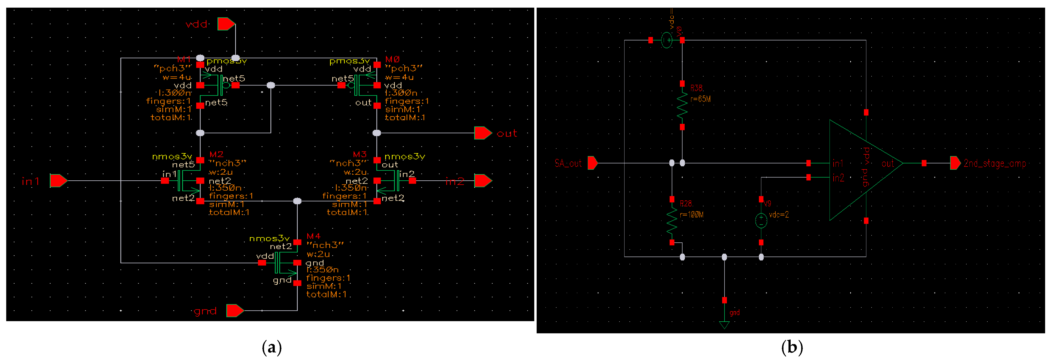
2.2. Amplification Stage
The AS is responsible for boosting the dynamic signal
f (
r) extracted from the SCS. This stage employs a differential amplifier configuration to ensure consistent and noise-immune signal amplification [
16]. To match the input signal level with the amplifier’s reference point, the output from the SCS is passed through a resistor divider network. One input of the DA receives the shifted signal via the resistor divider, while the other receives a fixed DC reference. This approach ensures that the signal is centered around a common mode before amplification, making the amplification process independent of variations introduced by different RCF levels.
This configuration ensures that all
f (
r) signals, regardless of
f (
m), are pulled to the same reference level before entering the DA. This standardization improves the robustness and reliability of the amplification process under diverse indoor conditions [
17]. As shown in the
Figure 5a the DA’s internal PMOS microdevices are sized at 4 µm width and 300 nm channel length, and 2 µm width with 350 nm channel length, optimized for gain and stability.
As shown in the
Figure 5b a DC reference of 2 V is chosen, and the resistor divider is designed using
R1 = 65 MΩ and
R2 = 100 MΩ, producing the desired 2 V from a 3.3 V supply. The voltage divider behavior is defined by the following formulas:
As shown in
Figure 6, the output waveforms, the signal from the SCS is successfully level- shifted to 2 V and cleanly amplified by the DA, and the representative 5 mV signal from the SCS with a pre-amplified value of 74.1 mV is amplified to 805 mV, while a 3 mV input signal corresponding to 43 mV is amplified to 588.68 mV [
17,
18]. The microsystem performs amplification for both 3 mV and 5 mV
f (
r) inputs, based on the applied signal. The amplified signal is now passed to the SPDS.
2.3. Stabilized Peak Detection Stage
The SPDS is designed to capture and hold the peak value of the amplified
f (
r) signal from the AS. This is essential for tracking the maximum observed SIR over a given interval, especially during rapidly changing light conditions due to various external factors. In this design, the SPDS consists of a single diode, resistor, and capacitor, forming a basic analog peak detector, as shown in
Figure 7a. The selected component values include a 5 pF capacitor and a 40 MΩ resistor, which together define the RC time constant that controls the charging rate and the stability of the present voltage [
19].
The diode conducts during the positive half-cycles of the input
f (
r), allowing for the capacitor to charge to the peak voltage level. When the input falls below this stored level, the diode is reverse-biased, effectively isolating the capacitor and holding the peak voltage [
20]. Over several cycles, the capacitor voltage stabilizes at the peak value of the signal minus the forward voltage drop of the diode. In this case, a diode with a forward drop of 0.6 V was used, which results in the SPDS output stabilizing just below the actual peak. Across all simulations with different signal amplitudes, the forward voltage drop remains consistent, with only minimal variation (±0.02 V). However, to further reduce this voltage drop at the SPDS, future system versions may incorporate a Schottky diode with a lower forward voltage drops (~0.2–0.3 V), or an op-amp buffer peak detection circuit to lower the forward voltage drop and enhance signal integrity.
Functionally, the SPDS behaves like a half-wave rectifier with an added filter capacitor, but instead of providing power, it stores peak signal information. This peak-hold behavior is critical in RGHE detection, where tracking the highest incident SIR is required. As shown in the output waveforms in
Figure 7b, the SPDS reliably captures and maintains peak amplitudes for 3 mV, 4 mV, and 5 mV input signals, validating its effectiveness in the proposed architecture [
21].
3. Integration of RGHE Microsystem and Analysis
The integrated RGHE detection system brings together the SCS, AS, and SPDS to accurately sense, isolate, amplify, and retain the dynamic sunlight intensity signal
f (
r), while effectively rejecting the static room condition factor
f (
m) [
22]. As illustrated in
Figure 8, the SCS is configured as an operational amplifier with a feedback resistor
Rf = 100 kΩ and an input resistor
Rin = 5 kΩ. This stage isolates
f (
r) from the composite input signal received from the LDR, which initially includes both
f (
r) and
f (
m).
The output of the SCS is passed to the AS through a resistor divider network, which shifts the signal level appropriately. This divider consists of R1 = 65 MΩ and R2 = 100 MΩ, chosen to produce a reference voltage of 2 V from a 3.3 V supply. This ensures that the amplified signal remains centered and consistent across different operating conditions.
The amplified signal is then directed to the SPDS, which consists of a 5 pF capacitor and a 40 MΩ resistor in combination with a diode. This stage acts as a peak detector, capturing and holding the maximum value of the amplified
f (
r) signal [
23]. The diode conducts during the positive half-cycle, charging the capacitor, while the resistor determines the discharge rate and stabilization time. This complete pipeline ensures robust RGHE monitoring by isolating dynamic solar inputs and maintaining peak signal information, even under varying illumination and environmental conditions.
As shown in the output waveforms in
Figure 9, the red signal represents the composite input to the integrated circuit, which includes both the dynamic sunlight intensity component
f (
r) and the static room condition factor
f (
m). The green waveform illustrates the output from the SCS, where
f (
r) is successfully isolated and level-shifted to 2 V through the operational amplification process [
24]. The light blue waveform corresponds to the output from the AS, where the extracted
f (
r) signal is amplified to a suitable range for final processing. Finally, the dark blue waveform displays the output of the SPDS, which holds the detected peak value of the amplified
f (
r), ensuring that the maximum SIR level is accurately captured over time. This multi-stage output demonstrates the correct functioning of the entire analog processing system [
25].
Figure 9a shows the waveform for a 3 mV
f (
r) and 0.75 V
f (
m) input signal [
26].
After processing through the SCS, the isolated output is 44.4 mV, which is further amplified to 580.26 mV in the AS. The SPDS then detects a peak value of 1.6934 V, stabilizing at approximately 60.77 µs. Similarly, for a 3 mV f (r) and 1 V f (m) input, the peak is detected at 1.6976 V. These results demonstrate that regardless of the DC bias f (m), the system consistently amplifies and detects the same signal f (r). Furthermore, for a 4 mV f (r) with 1 V f (m), the peak is recorded at 1.8369 V, while for a 5 mV f (r) with 0.75 V f (m), the peak reaches 1.9136 V. Across all test cases, the output peaks stabilize within approximately 60 µs, indicating that the capacitor in the SPDS takes about 60 µs to fully charge. All the x-axes represent time in microseconds, and the y-axes represent voltage in volts. The SC consumed approximately 116.89 µW, while the AS, comprising the gain amp and resistor divider, drew around 204.94 µW. The SPDS, built using a diode configuration with an RC holding network, consumed roughly 50.16 µW during dynamic signal tracking. In total, the power consumption across these three analog subsystems is approximately 370 µW, supporting the design’s practicality and suitability for low-power, real-time analog signal processing applications.
All measured combinations of
f (
r) and
f (
m) signals, along with corresponding outputs from the SCS, AS, and SPDS, are summarized in
Table 2. As shown in
Figure 10, all the graphical representations of the SCS, AS, and SPDS outputs show that the values of
f (
r) remain consistent in each corresponding value of
f (
m).
RGHE Intensity Estimation from SPDS Output
From the graphical and tabular results, it is observed that the SPDS output peak voltage strongly correlates with the dynamic sunlight intensity component
f (
r), while remaining largely unaffected by the static room bias
f (
m) [
27]. This behavior ensures reliable isolation and detection of RGHE across varying room environments [
28].
To model this relationship, polynomial equations were fitted to the SPDS output graph for two representative
f (
r) values:
The difference between the two output levels (i.e., for a 2 mV increase in
f (
r)) is approximated by
This voltage difference corresponds to a 60% increase in effective SIR (from 20% at 3 mV to 80% at 5 mV). Based on simplified linear calibration, each 10% increment is considered to correspond to a 0.333 mV rise in SPDS peak voltage [
29,
30,
31,
32,
33]. Thus, if the detected SPDS peak is 3.5 mV and the baseline is 3.0 mV, the increase is
Therefore, the estimated total RGHE intensity is
So, this method enables direct mapping of the detected SPDS output voltage to the RGHE intensity level, allowing for accurate, real-time interpretation of indoor solar loading for a smart climate-responsive microsystem.
4. Layout Considerations
All circuits were implemented using the TSMC 180 nm technology library, with their corresponding layouts developed as part of the overall integrated circuit design. The layout design followed a process technology with a feature size of
λ = 90 nm. Pads were incorporated to serve as interfacing elements between the internal circuitry and the external environment, enabling signal communication and power delivery. Each pad measures 70 µm × 70 µm in size. In CMOS processes like TSMC 180 nm, gate oxide breakdown voltages range between 5 and 7 V, while Electrostatic Discharge (ESD) events such as those modeled by the Human Body Model (HBM) can reach up to 3500 V, which can irreparably damage thin gate oxides. To prevent this, ESD protection diodes were designed for each pad. These pads are constructed by stacking all six available metal layers vertically, interconnected using vias (via12, via23, …, via56). Metal 1 extends inward to connect to internal circuit nodes. The ESD diodes are connected between VDD and GND, ensuring that voltage spikes are safely redirected—positive transients are clamped to GND, and negative transients to VDD [
34]. The system was fabricated through MUSE Semiconductors and packaged in a QP-QFN32 5 mm × 5 mm package, as shown in
Figure 11.
The padframe, composed of 32 connection pads, incorporates VDD and GND rails routed on Metal 5 and Metal 6 with a width of 40
λ [
35]. These power lines are symmetrically distributed along the periphery of the padframe to ensure consistent power and ground access [
36,
37,
38,
39]. Proper placement of internal components within the padframe is critical to maintain signal integrity, balance power delivery, and simplify routing complexity. The full integrated circuit module is centrally located within the padframe to optimize performance and reliability. Additionally, some individual sub-circuits were laid out separately within the system for isolated testing. Signal lines routed over long distances from the pads to internal blocks were widened to minimize resistance, while VDD and GND traces were designed to be wider (approximately 3–4 µm) than regular signal lines to handle the higher current demands of the entire IC. Once initial testing and validation of the chip are complete, the unit cost can be significantly reduced through bulk production to an estimated price point of approximately USD 1.50 per chip in high-volume fabrication runs.
5. Future Work
To evaluate sensor flexibility, the system will be tested with alternative photodetectors such as LDRs, photodiodes, and phototransistors. Additionally, an on-chip calibration circuit will be developed to automatically estimate and adjust for the static room condition factor f(m), ensuring consistent performance across diverse indoor environments. To improve peak detection accuracy, the current SPDS will be upgraded using a Schottky diode with a lower forward voltage drop or an op-amp-based peak detection circuit, reducing output variations caused by diode non-idealities.
The next phase will involve experimental validation of the fabricated chip, comparing its performance against pre-silicon simulation results to assess accuracy, stability, and robustness. We also plan to migrate the design to an advanced CMOS process node, which will reduce area, lower power consumption, and support denser integration. Furthermore, wireless transmission capabilities will be integrated to enable real-time data monitoring and support seamless deployment in smart building applications.
In parallel, the system’s behavior under non-ideal real-world conditions will be rigorously analyzed. This includes assessing the effects of environmental noise such as ambient light flicker, and temperature variations, which may influence signal stability. Additionally, the role of component tolerances, fabrication process variations, and physical noise sources (thermal, flicker, shot noise) will be modeled and experimentally validated. These efforts will guide the development of a more robust, noise-tolerant analog architecture capable of maintaining high accuracy in indoor environments.
6. Conclusions
The proposed fully analog microsystem architecture effectively addresses the challenges of detecting the RGHE by isolating and tracking the SIR in real time. The microsystem comprises three integrated stages, SCS, AS, and SPDS, each contributing to accurate extraction, amplification, and storage of the dynamic sunlight signal f (r) while rejecting the static RCFs denoted as f (m). The system was tested across representative DC bias levels of f (m) = 0.75 V, 1.0 V, and 1.5 V and AC inputs of f (r) = 3 mV, 4 mV, and 5 mV. The SCS successfully isolated f (r), yielding output voltages in the range of 43–73 mV. These signals were further amplified by the AS to 580–814 mV. The SPDS then held peak voltages between 1.69 V and 1.92 V, with signal stabilization achieved within 60 µs, confirming the system’s responsiveness and precision. A calibrated polynomial model was developed to map SPDS output to RGHE intensity and determined that each 0.33 V increment in peak voltage equates to a 10% increase in effective RGHE exposure, enabling real-time percentage-based thermal impact estimation. The designed microsystem, implemented using TSMC 180 nm technology, offers a scalable solution for localized thermal monitoring in smart building environments using compact analog circuitry. The architecture can be scalable to different CMOS technology nodes, enabling trade-offs between power, area, and performance. For example, while the current design uses the TSMC 180 nm node for its analog performance and ease of prototyping, the same system could be migrated to more advanced nodes (e.g., 130 nm or 65 nm) for reduced area and power consumption in high-volume or integration into larger environmental sensing systems. The results demonstrate the feasibility of deploying a micro-design solution for environmental sensing and energy optimization.


 —composite input from sensor;
  —SCS output isolating f (r);
  —AS output amplifying f (r);
  —SPDS output showing peak detection.


