
Non-Destructive Characterization of Selected Types of Films and Other Layers via White Light Reflectance Spectroscopy (WLRS)

 ,
, 

Abstract
:1. Introduction
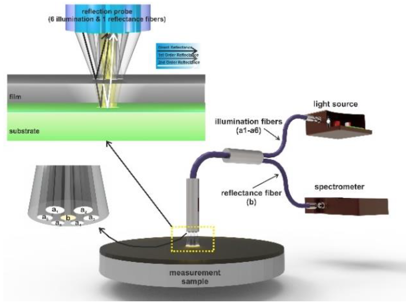
2. WLRS Methodology
3. Results and Discussion
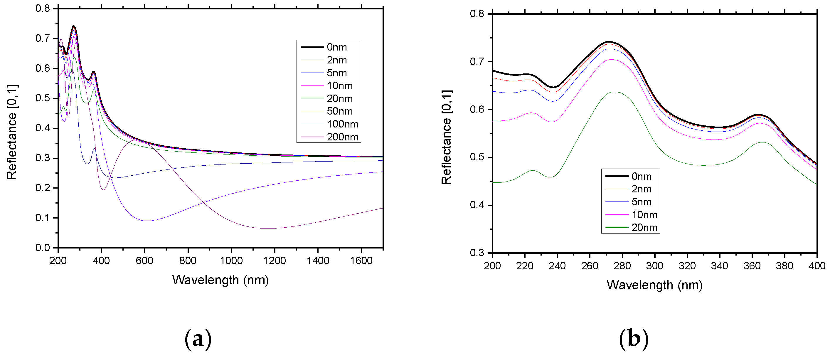
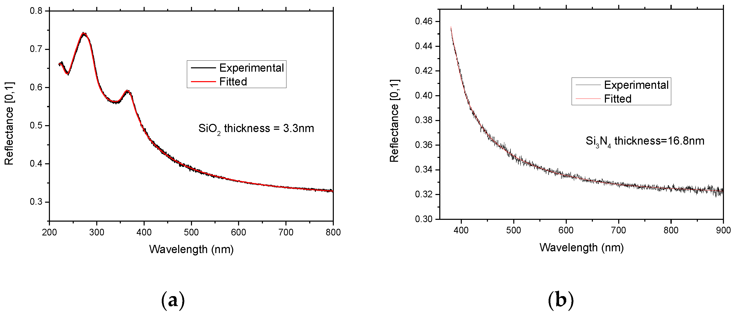
3.1. Characterization of Ultra-Thin Films
3.2. Characterization of 2D Materials
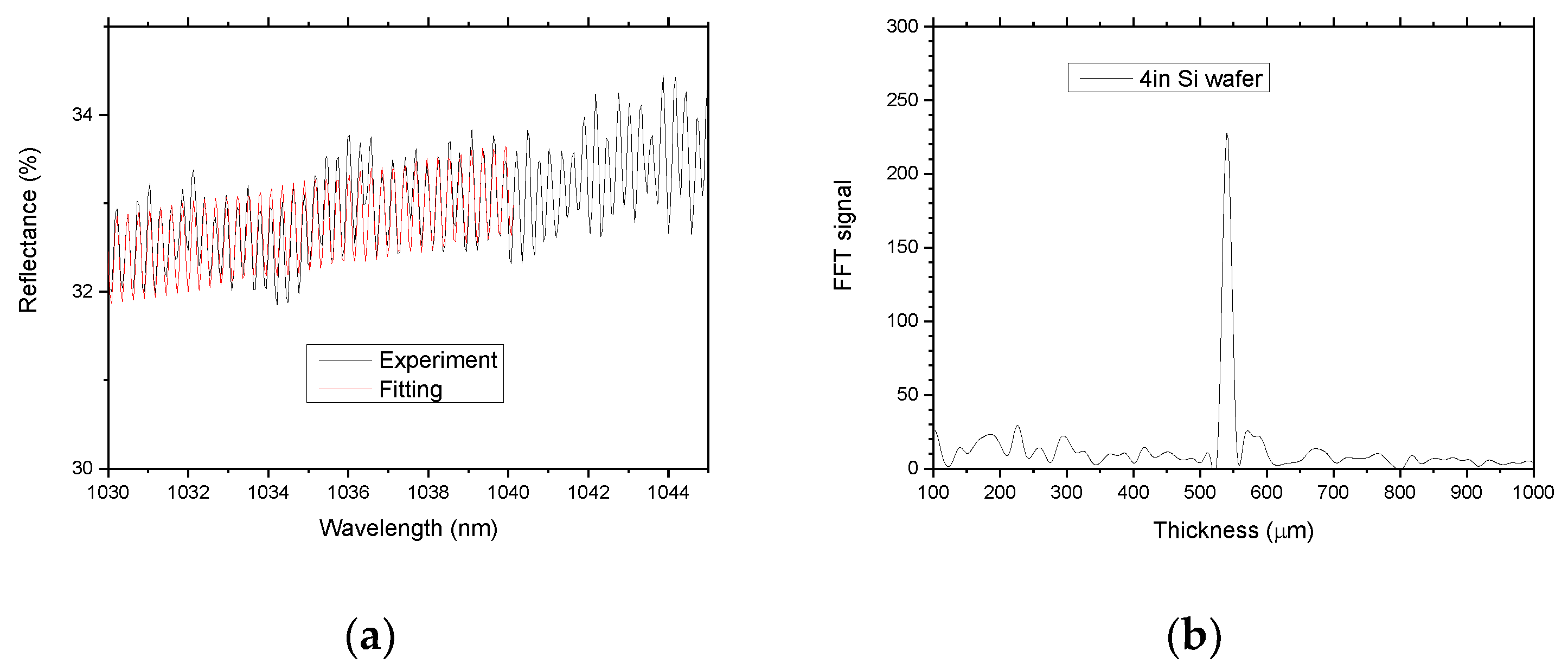
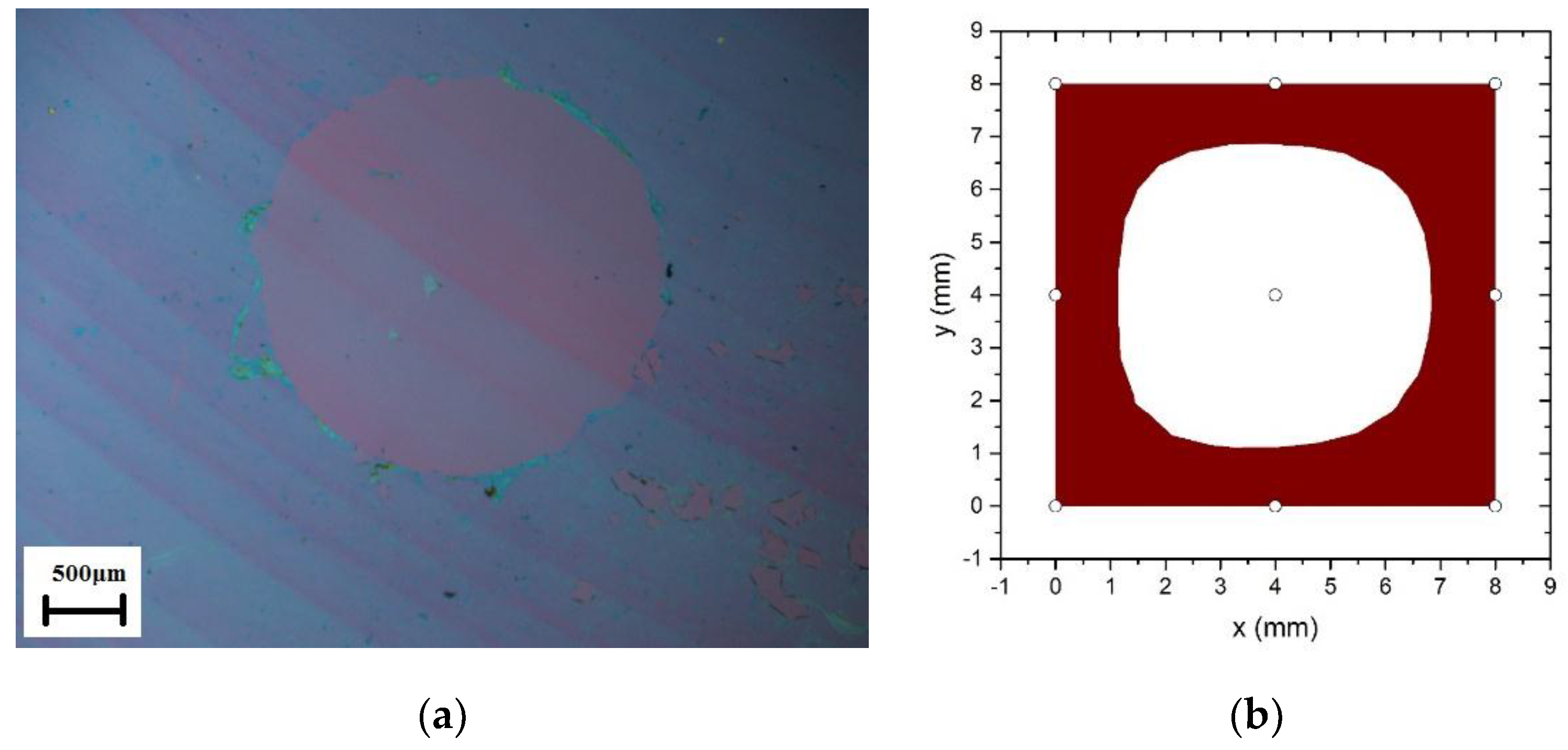
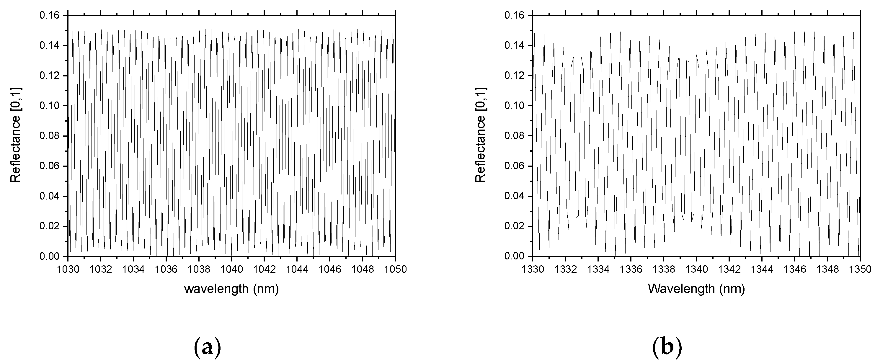
3.3. Characterization of Ultra-Thick Films
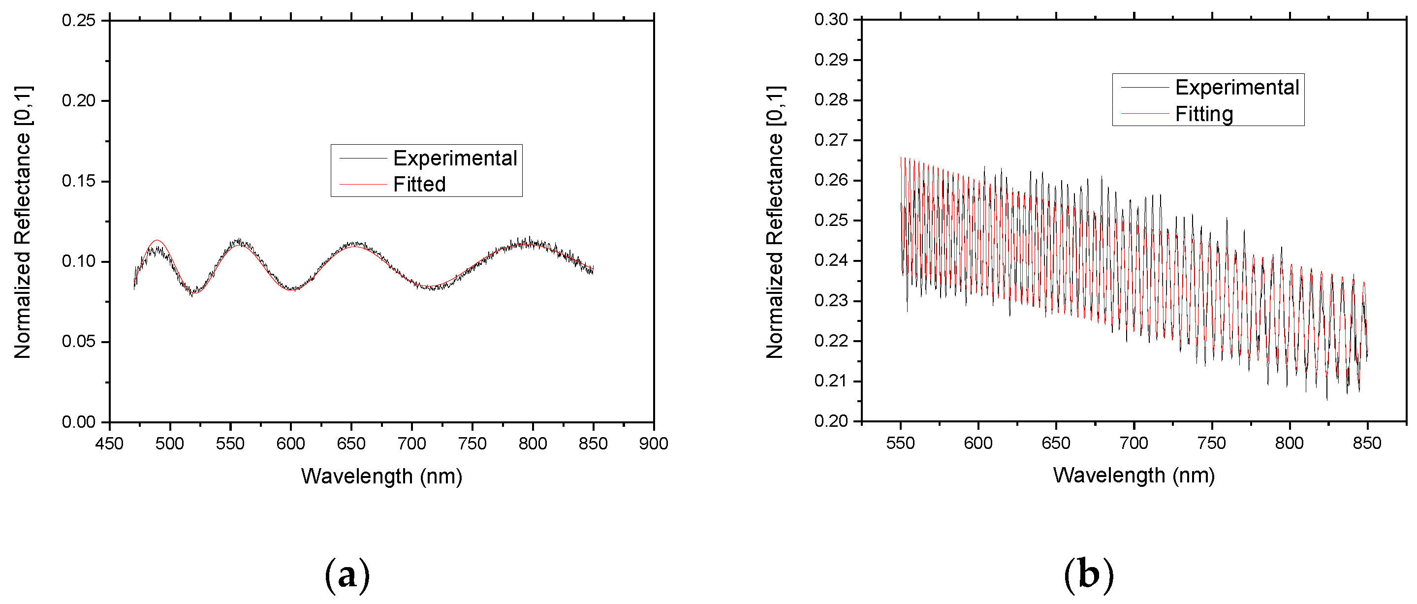
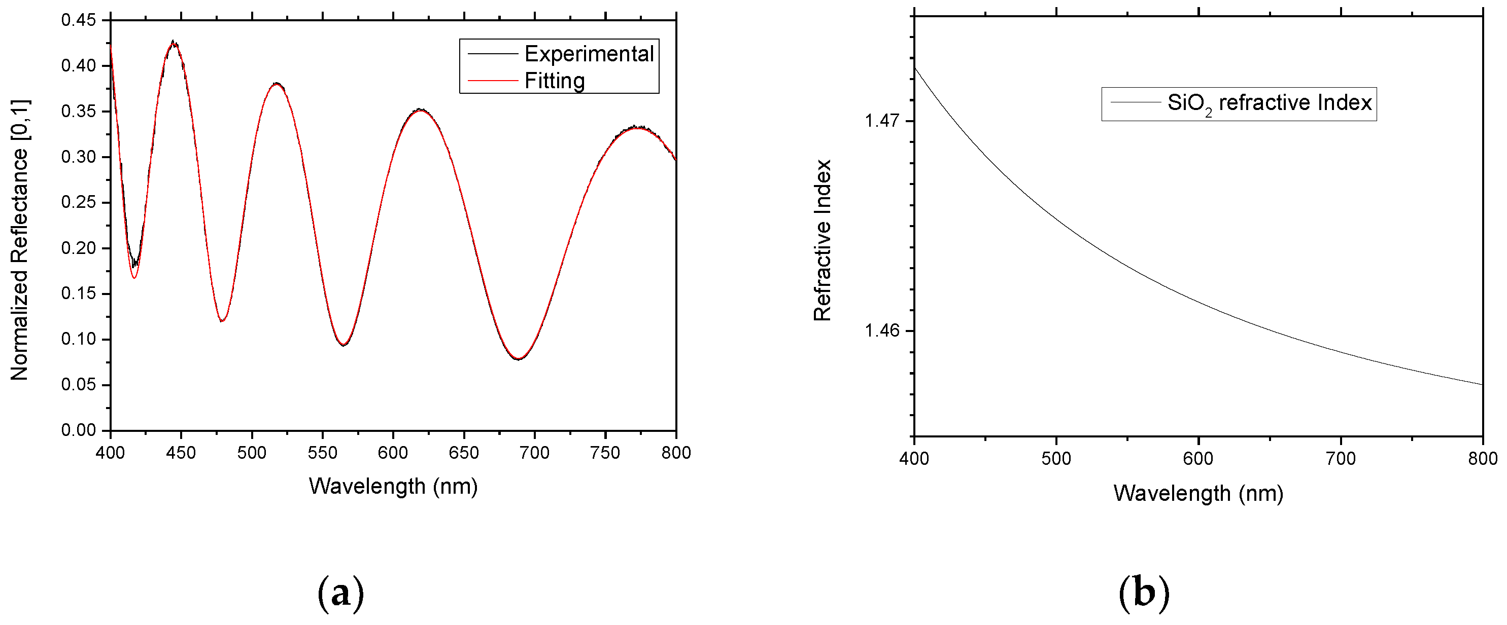
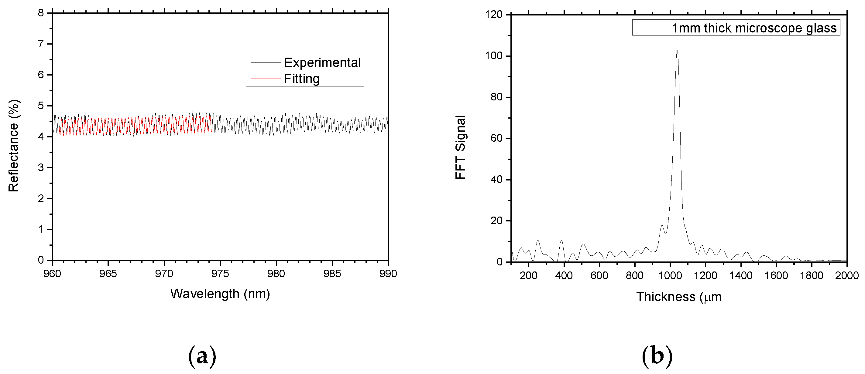
3.4. Characterization of Transparent Layers on Transparent Substrates
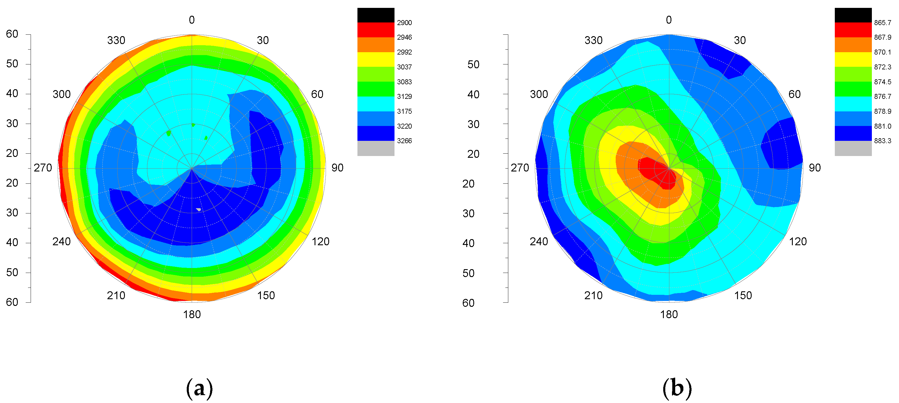
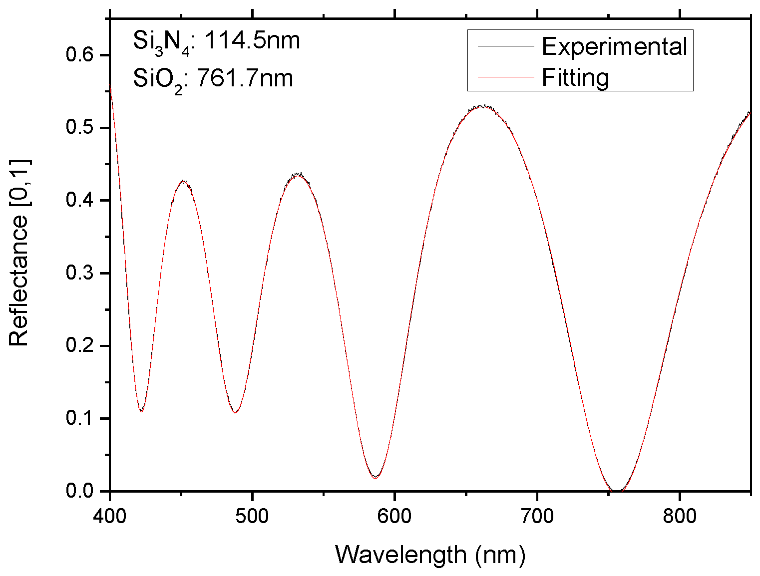
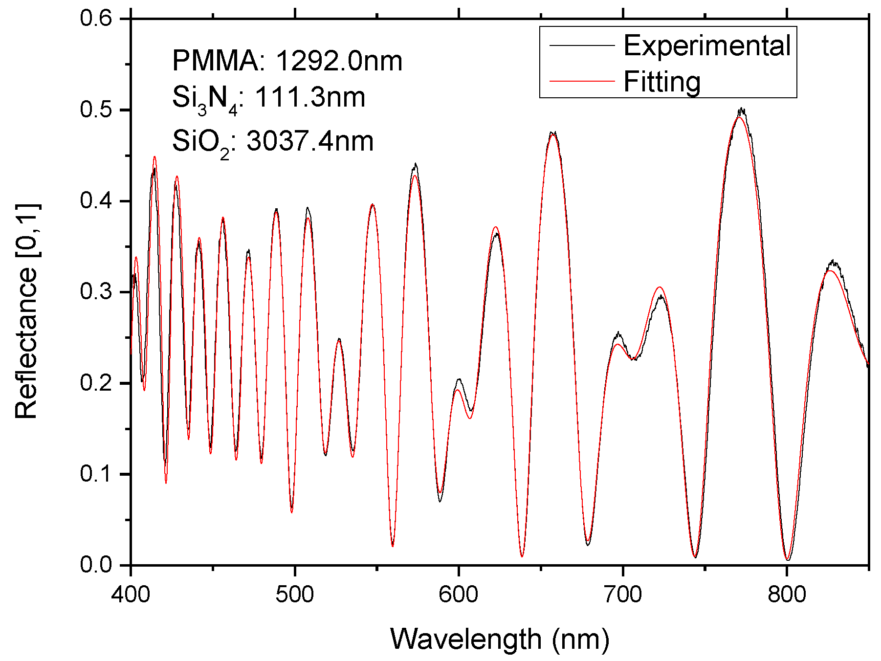
3.5. Multi-Layer Films
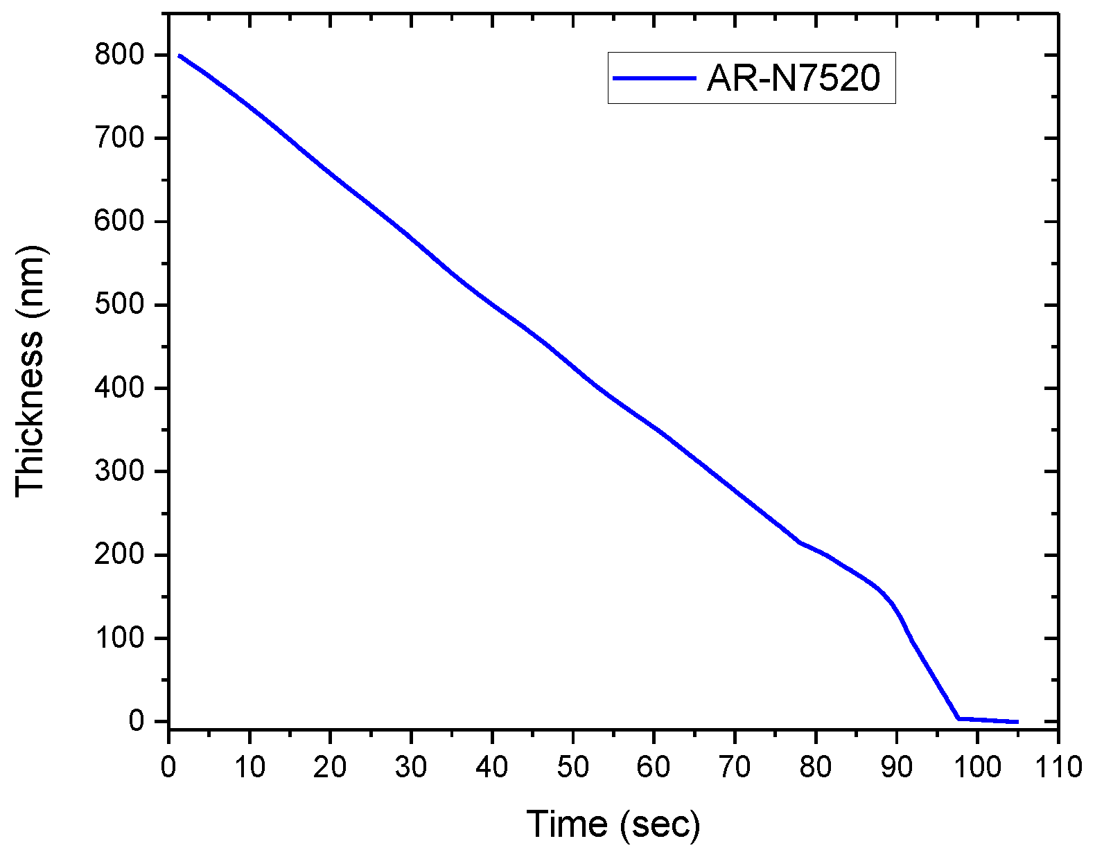
3.6. Kinetics of Chemical and Physical Chemical Processes and Monitoring of Transitions
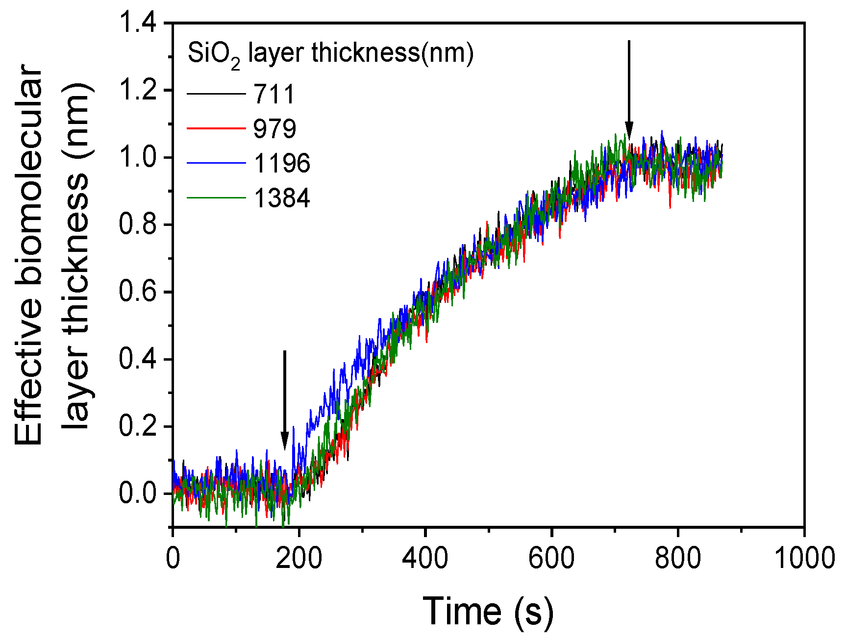
3.7. In Situ Monitoring of Biomolecular Interactions
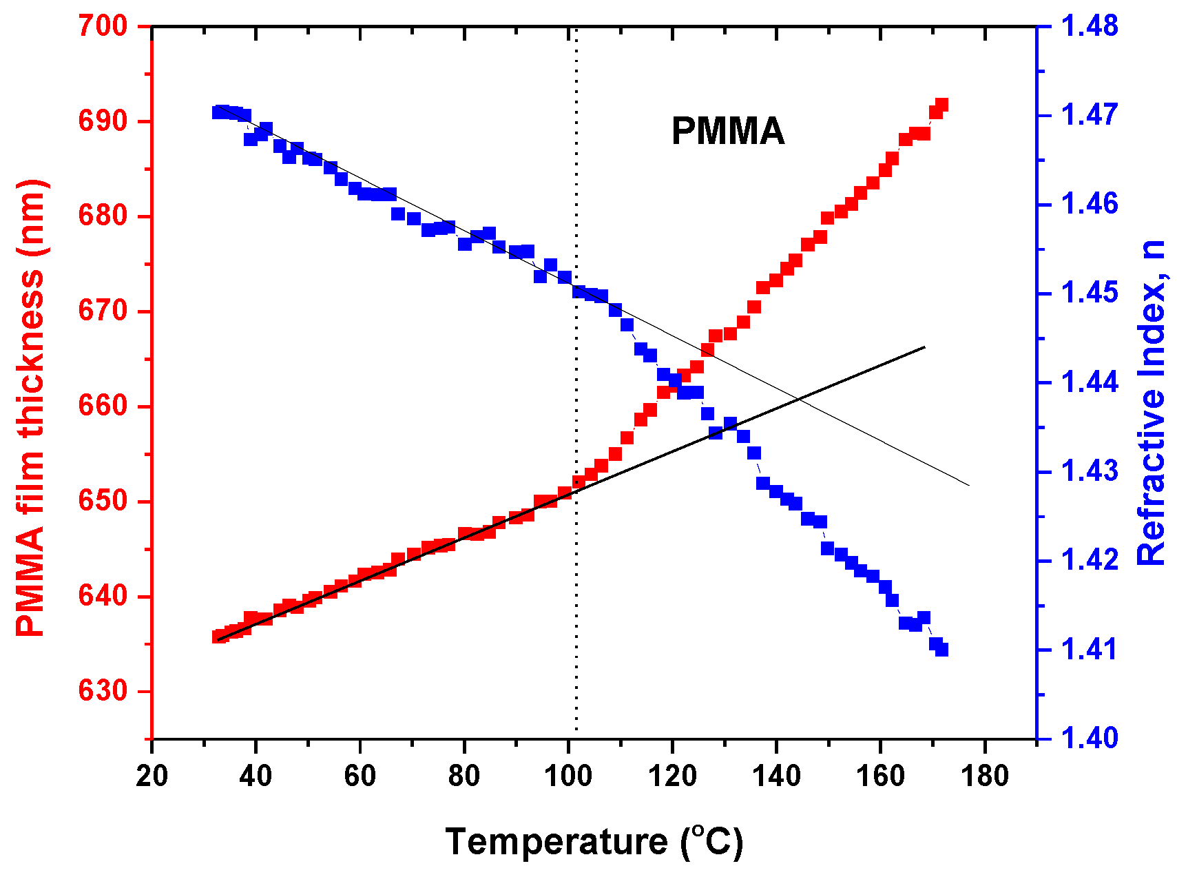
3.8. Refractive Index Measurement
4. Conclusions
Author Contributions
Funding
Data Availability Statement
Conflicts of Interest
References
- Stenzel, O.; Ohlídal, M. (Eds.) Optical Characterization of Thin Solid Films, 1st ed.; Springer Series in Surface Sciences; Springer: Berlin/Heidelberg, Germany, 2018; Volume 64. [Google Scholar]
- Tompkins, H.G.; Hilfiker, J.N. Spectroscopic Ellipsometry: Practical Application to Thin Film Characterization; Materials Characterization and Analysis Collection; Momentum Press: New York, NY, USA, 2015. [Google Scholar]
- Quinten, M. A Practical Guide to Optical Metrology for Thin Films, 1st ed.; Wiley-VCH: Weinheim, Germany, 2012. [Google Scholar]
- Gujrati, A.; Khanal, S.R.; Pastewka, L.; Jacobs, T.D.B. Combining TEM, AFM, and Profilometry for Quantitative Topography Characterization Across All Scales. ACS Appl. Mater. Interfaces 2018, 10, 29169–29178. [Google Scholar] [CrossRef] [PubMed]
- Lu, M.; Chen, L.; Meng, X.; Huang, R.; Peyton, A.; Yin, W. Thickness Measurement of Metallic Film Based on a High-Frequency Feature of Triple-Coil Electromagnetic Eddy Current Sensor. IEEE Trans. Instrum. Meas. 2021, 70, 6001208. [Google Scholar] [CrossRef]
- Lammel, M.; Geishendorf, K.; Choffel, M.A.; Hamann, D.M.; Johnson, D.C.; Nielsch, K.; Thomas, A. Fast Fourier transform and multi-Gaussian fitting of XRR data to determine the thickness of ALD grown thin films within the initial growth regime. Appl. Phys. Lett. 2020, 117, 213106. [Google Scholar] [CrossRef]
- Hasan, M.; Lyon, K.; Trombley, L.; Smith, C.; Zakhidov, A. Thickness measurement of multilayer film stack in perovskite solar cell using spectroscopic ellipsometry. AIP Adv. 2019, 9, 125107. [Google Scholar] [CrossRef]
- Hao, R.; Zhu, L.; Li, Z.; Fang, F.; Zhang, X. A Miniaturized and Fast System for Thin Film Thickness Measurement. Appl. Sci. 2020, 10, 7284. [Google Scholar] [CrossRef]
- Frisenda, R.; Niu, Y.; Gant, P.; Molina-Mendoza, A.J.; Schmidt, R.; Bratschitsch, R.; Liu, J.; Fu, L.; Dumcenco, D.; Kis, A.; et al. Micro-reflectance and transmittance spectroscopy: A versatile and powerful tool to characterize 2D materials. J. Phys. D Appl. Phys. 2017, 50, 074002. [Google Scholar] [CrossRef]
- Bosch, S.; Monzonis, F. General inversion method for single-wavelength ellipsometry of samples with an arbitrary number of layers. J. Opt. Soc. Am. A 1995, 12, 1375–1379. [Google Scholar] [CrossRef]
- Aspnes, D. Spectroscopic ellipsometry—Past, present, and future. Thin Solid Films 2014, 571, 334–344. [Google Scholar] [CrossRef]
- Heavens, O.S. Optical Properties of Thin Solid Films, 2nd ed.; Dover: New York, NY, USA, 2011. [Google Scholar]
- Luňáček, J.; Hlubina, P.; Luňáčková, M. Simple method for determination of the thickness of a nonabsorbing thin film using spectral reflectance measurement. Appl. Opt. 2009, 48, 985–989. [Google Scholar] [CrossRef] [PubMed]
- Kitsara, M.; Petrou, P.; Kontziampasis, D.; Misiakos, K.; Makarona, E.; Raptis, I.; Beltsios, K. Biomolecular layer thickness evaluation using White Light Reflectance Spectroscopy. Microelectron. Eng. 2010, 87, 802–805. [Google Scholar] [CrossRef]
- Lubecke, V.M.; Pardo, F.; Lifton, V.A. Polyimide Spacers for Flip-Chip Optical MEMS. J. Microelectromech. Syst. 2007, 16, 959–968. [Google Scholar] [CrossRef]
- Park, J.; Kim, J.-A.; Ahn, H.; Bae, J.; Jin, J. A Review of Thickness Measurements of Thick Transparent Layers Using Optical Interferometry. Int. J. Precis. Eng. Manuf. 2019, 20, 463–477. [Google Scholar] [CrossRef]
- Bellavia, S.; Gratton, S.; Riccietti, E. A Levenberg-Marquardt method for large nonlinear least-squares problems with dynamic accuracy in functions and gradients. Numer. Math. 2018, 140, 791–825. [Google Scholar] [CrossRef]
- Matenaers, C.; Popper, B.; Rieger, A.; Wanke, R.; Blutke, A. Practicable methods for histological section thickness measurement in quantitative stereological analyses. PLoS ONE 2018, 13, e0192879. [Google Scholar] [CrossRef] [PubMed]
- Mohammadigharehbagh, R.; Pat, S.; Özen, S.; Yudar, H.H.; Korkmaz, S. Investigation of the optical properties of the indium-doped ZnO thin films deposited by a thermionic vacuum arc. Optik 2018, 157, 667–674. [Google Scholar] [CrossRef]
- Jin, P.; Xu, G.; Tazawa, M.; Yoshimura, K. Design, formation and characterization of a novel multifunctional window with VO2 and TiO2 coatings. Appl. Phys. A 2003, 77, 455–459. [Google Scholar] [CrossRef]
- Chiappelli, M.C.; Hayward, R.C. Photonic Multilayer Sensors from Photo-Crosslinkable Polymer Films. Adv. Mater. 2012, 24, 6100–6104. [Google Scholar] [CrossRef]
- Mpatzaka, T.; Papageorgiou, G.; Papanikolaou, N.; Valamontes, E.; Ganetsos, T.; Goustouridis, D.; Raptis, I.; Zisis, G. In-situ characterization of the development step of high-resolution e-beam resists. Microelectron. Eng. 2020, 9, 100070. [Google Scholar] [CrossRef]
- Vourdas, N.; Karadimos, G.; Goustouridis, D.; Gogolides, E.; Boudouvis, A.G.; Tortai, J.-H.; Beltsios, K.; Raptis, I. Multi-wavelength interferometry and competing optical methods for the thermal probing of thin polymeric films. J. Appl. Polym. Sci. 2006, 102, 4764–4774. [Google Scholar] [CrossRef]
- Oizumi, H.; Tanaka, K.; Kawakami, K.; Itani, T. Development of New Positive-Tone Molecular Resists Based on Fullerene Derivatives for Extreme Ultraviolet Lithography. Jpn. J. Appl. Phys. 2009, 116, 184–190. [Google Scholar] [CrossRef]
- Manoli, K.; Goustouridis, D.; Raptis, I.; Valamontes, E.; Sanopoulou, M. Vapor-induced swelling of supported methacrylic and siloxane polymer films: Determination of interaction parameters. J. Appl. Polym. Sci. 2010, 116, 184–190. [Google Scholar] [CrossRef]
- Chapman, M.; Mullen, M.; Novoa-Ortega, E.; Alhasani, M.; Elman, J.F.; Euler, W.B. Structural Evolution of Ultrathin Films of Rhodamine 6G on Glass. J. Phys. Chem. C 2016, 120, 8289–8297. [Google Scholar] [CrossRef]
- Koukouvinos, G.; Petrou, P.; Misiakos, K.; Drygiannakis, D.; Raptis, I.; Stefanitsis, G.; Martini, S.; Nikita, D.; Goustouridis, D.; Moser, I.; et al. Simultaneous determination of CRP and D-dimer in human blood plasma samples with White Light Reflectance Spectroscopy. Biosens. Bioelectron. 2016, 84, 89–96. [Google Scholar] [CrossRef] [PubMed]
- Abdiche, Y.; Malashock, D.; Pinkerton, A.; Pons, J. Determining kinetics and affinities of protein interactions using a parallel real-time label-free biosensor, the Octet. Anal. Biochem. 2008, 377, 209–217. [Google Scholar] [CrossRef] [PubMed]
- Anastasiadis, V.; Koukouvinos, G.; Petrou, P.S.; Economou, A.; Harjanne, M.; Heimala, P.; Goustouridis, D.; Raptis, I.; Kakabakos, S.E. Multiplexed mycotoxins determination employing white light reflectance spectroscopy and silicon chips with silicon oxide areas of different thickness. Biosens. Bioelectron. 2020, 153, 112035. [Google Scholar] [CrossRef] [PubMed]
- Petrou, P.S.; Ricklin, D.; Zavali, M.; Raptis, I.; Kakabakos, S.E.; Misiakos, K.; Lambris, J.D. Real-time label-free detection of complement activation products in human serum by white light reflectance spectroscopy. Biosens. Bioelectron. 2009, 24, 3359–3364. [Google Scholar] [CrossRef] [PubMed]
- Koukouvinos, G.; Petrou, P.S.; Misiakos, K.; Drygiannakis, D.; Raptis, I.; Goustouridis, D.; Kakabakos, S.E. A label-free flow-through immunosensor for determination of total- and free-PSA in human serum samples based on white-light reflectance spectroscopy. Sens. Actuator B 2015, 209, 1041–1048. [Google Scholar] [CrossRef]


Publisher’s Note: MDPI stays neutral with regard to jurisdictional claims in published maps and institutional affiliations. |
© 2022 by the authors. Licensee MDPI, Basel, Switzerland. This article is an open access article distributed under the terms and conditions of the Creative Commons Attribution (CC BY) license (https://creativecommons.org/licenses/by/4.0/).
Share and Cite
Goustouridis, D.; Raptis, I.; Mpatzaka, T.; Fournari, S.; Zisis, G.; Petrou, P.; Beltsios, K.G. Non-Destructive Characterization of Selected Types of Films and Other Layers via White Light Reflectance Spectroscopy (WLRS). Micro 2022, 2, 495-507. https://doi.org/10.3390/micro2030031
Goustouridis D, Raptis I, Mpatzaka T, Fournari S, Zisis G, Petrou P, Beltsios KG. Non-Destructive Characterization of Selected Types of Films and Other Layers via White Light Reflectance Spectroscopy (WLRS). Micro. 2022; 2(3):495-507. https://doi.org/10.3390/micro2030031
Chicago/Turabian StyleGoustouridis, Dimitrios, Ioannis Raptis, Theodora Mpatzaka, Savvina Fournari, Grigorios Zisis, Panagiota Petrou, and Konstantinos G. Beltsios. 2022. "Non-Destructive Characterization of Selected Types of Films and Other Layers via White Light Reflectance Spectroscopy (WLRS)" Micro 2, no. 3: 495-507. https://doi.org/10.3390/micro2030031
APA StyleGoustouridis, D., Raptis, I., Mpatzaka, T., Fournari, S., Zisis, G., Petrou, P., & Beltsios, K. G. (2022). Non-Destructive Characterization of Selected Types of Films and Other Layers via White Light Reflectance Spectroscopy (WLRS). Micro, 2(3), 495-507. https://doi.org/10.3390/micro2030031