
A Review of Nanostructure Coating Techniques to Achieve High-Precision Optical Fiber Sensing Applications


Abstract
1. Introduction


2. Optical Fiber Sensors (OFSs)
2.1. Optical Fiber Sensors Classification
2.2. Current Limitations and Challenges of Optical Fiber Sensing Technology
3. Nanostructures and Synthesis Methods
3.1. Classification of Nanostructures
3.2. Synthesis Methods of Nanostructures
4. Nanostructure Coating Techniques for Optical Fiber Sensors
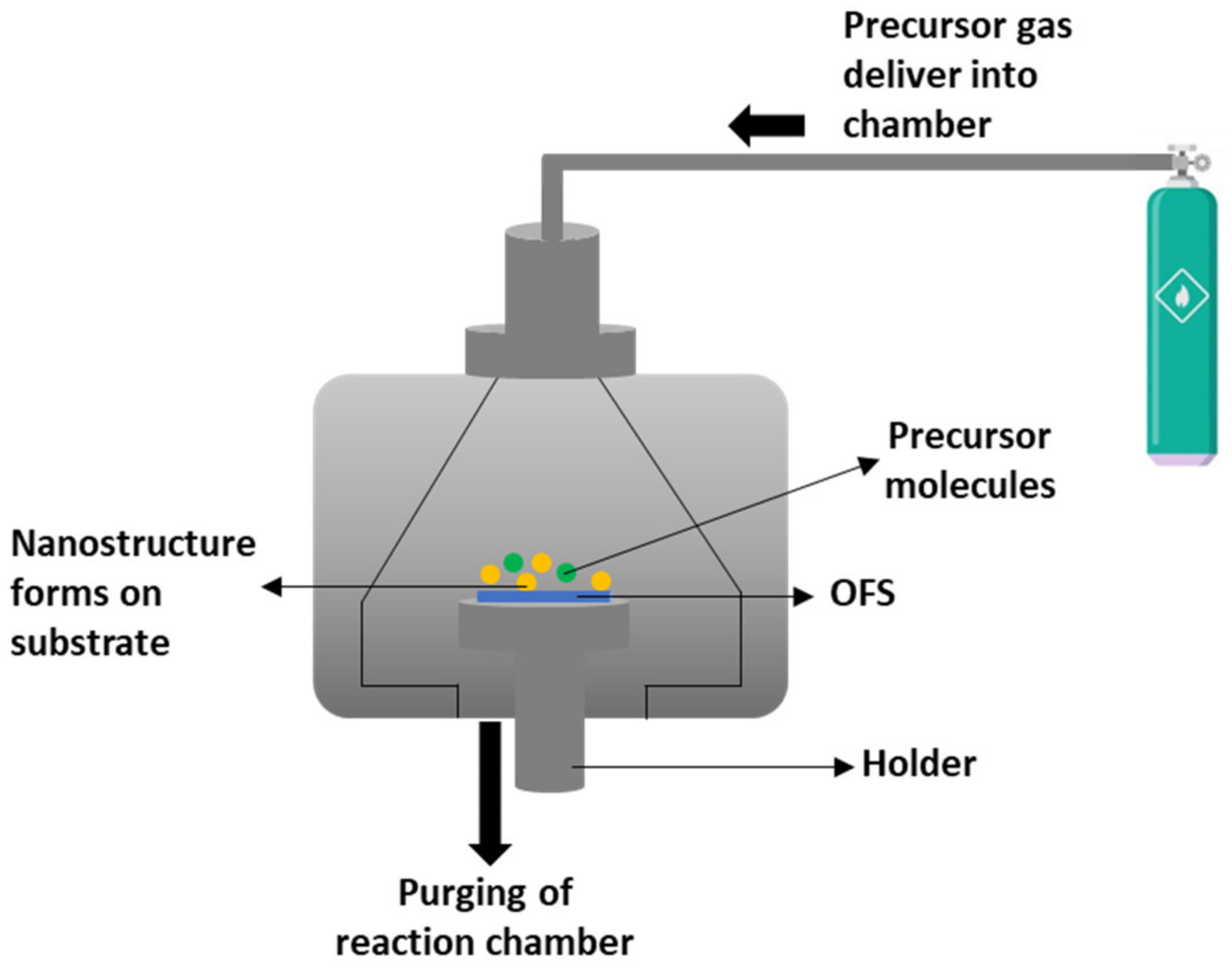
4.1. Chemical Vapor Deposition (CVD)
4.1.1. Metal–Organic Chemical Vapor Deposition (MOCVD)
4.1.2. Plasma-Enhanced Chemical Vapor Deposition (PECVD)

4.2. Atomic Layer Deposition (ALD)
4.3. Physical Vapor Deposition (PVD)
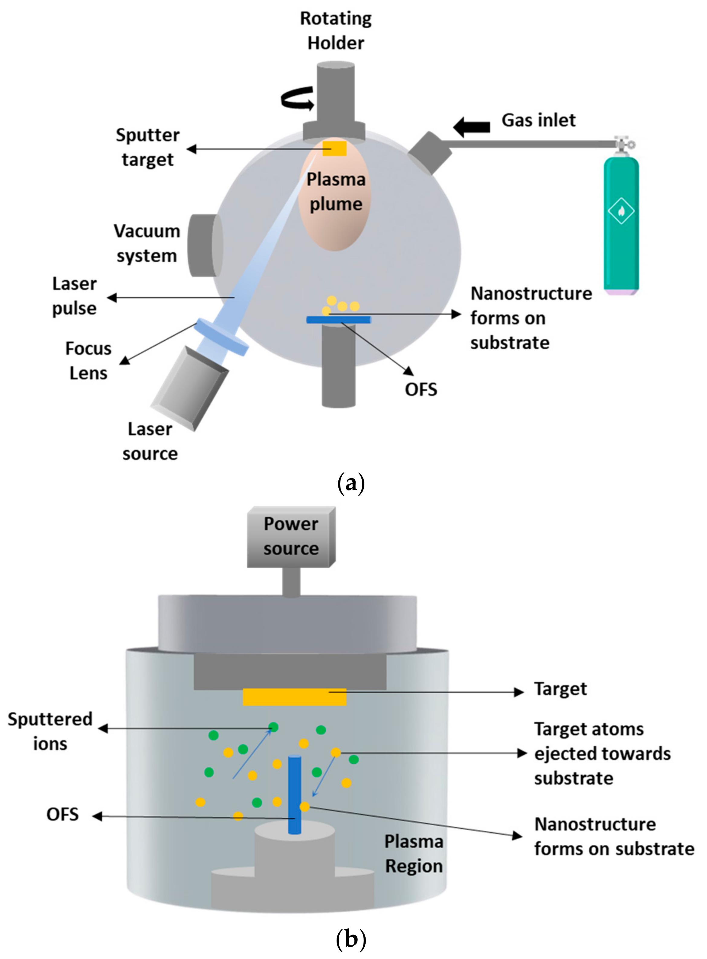
4.3.1. Magnetron Sputtering
4.3.2. DC Sputtering
4.3.3. RF Sputtering
4.3.4. Pulse Laser Deposition (PLD)
4.3.5. Thermal Evaporation
4.4. Dip Coating

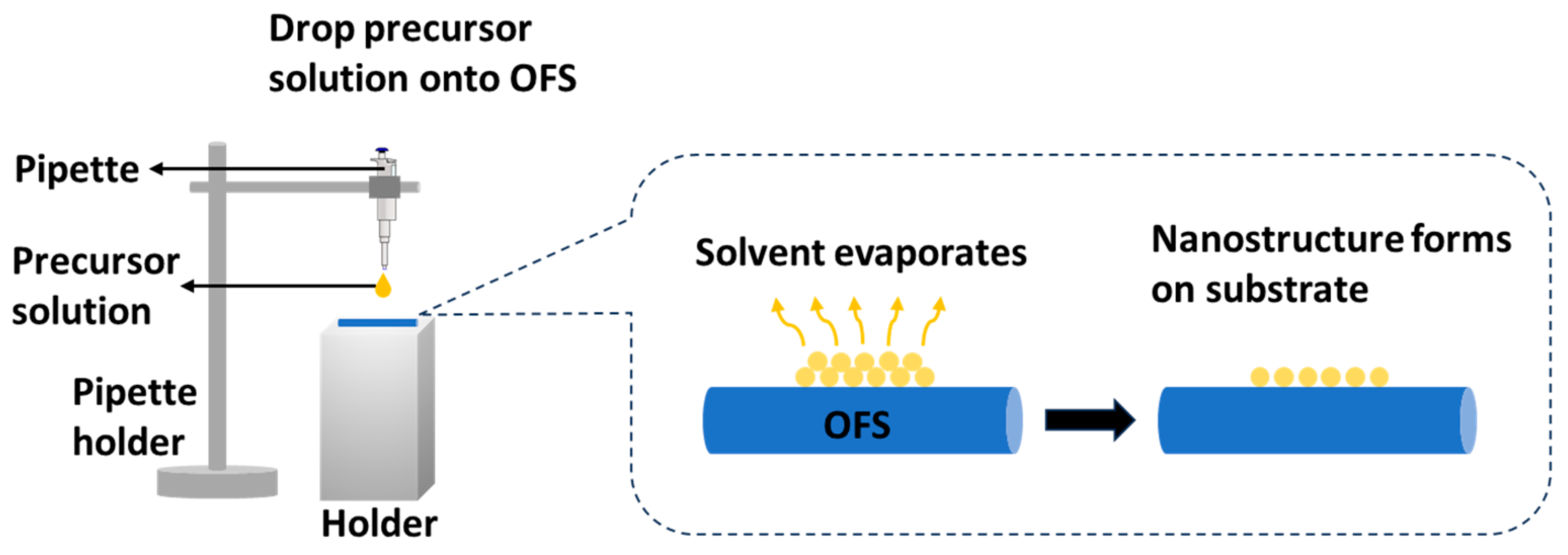
4.5. Drop Casting
5. High-Precision Optical Fiber Sensing with Nanostructure Coating
5.1. Key Coating Parameters
5.2. Advancement of Optical Fiber Sensing
5.2.1. Modification of Dimensional Nanostructure
5.2.2. Optimization of Coating Thickness and Coating Layer
6. Recommendations and Future Works
Author Contributions
Funding
Data Availability Statement
Conflicts of Interest
References
- Kaur, S.; Singh, P.; Tripathi, V.; Kaur, R. Recent trends in wireless and optical fiber communication. Glob. Transit. Proc. 2022, 3, 343–348. [Google Scholar] [CrossRef]
- Leal-Junior, A.; Silva, J.; Macedo, L.; Marchesi, A.; Morau, S.; Valentino, J.; Valentim, F.; Costa, M. The Role of Optical Fiber Sensors in the New Generation of Healthcare Devices: A Review. Sens. Diagn. 2024, 3, 1135–1158. [Google Scholar] [CrossRef]
- Zhang, H.; Liu, T.; Lu, J.; Lin, R.; Chen, C.; He, Z.; Cui, S.; Liu, Z.; Wang, X.; Liu, B.; et al. Static and ultrasonic structural health monitoring of full-size aerospace multi-function capsule using FBG strain arrays and PSFBG acoustic emission sensors. Opt. Fiber Technol. 2023, 78, 103316. [Google Scholar] [CrossRef]
- Zhu, T.; Shen, J.; Martin, E.R. Sensing earth and environment dynamics by telecommunication fiber-optic sensors: An urban experiment in Pennsylvania USA. Solid Earth Discuss. 2020, 12, 219–235. [Google Scholar] [CrossRef]
- Hossain, M.I.; Mansour, S. A critical overview of thin films coating technologies for energy applications. Cogent Eng. 2023, 10, 2179467. [Google Scholar] [CrossRef]
- Demircan, G.; Gurses, E.F.; Acikgoz, A.; Yalcin, S.; Aktas, B. Effects of spin coating parameters on stress, electrical and optical properties of multilayer ZnO thin film prepared by sol–gel. Mol. Cryst. Liq. Cryst. 2020, 709, 61–69. [Google Scholar] [CrossRef]
- Bhushan, T.; Chandrashekhar, A.; Prasat, S.V.; Reddy, I.R. Effect of substrate surface roughness on adhesion of titanium nitride coatings deposited by physical vapour deposition technique. IOP Conf. Ser. Mater. Sci. Eng. 2020, 981, 042022. [Google Scholar] [CrossRef]
- Hu, H.; Weibel, J.A.; Garimella, S.V. Role of nanoscale roughness in the heat transfer characteristics of thin film evaporation. Int. J. Heat Mass Transfer 2020, 150, 119306. [Google Scholar] [CrossRef]
- Ziti, A.; Hartiti, B.; Belafhaili, A.; Labrim, H.; Fadili, S.; Ridah, A.; Tahri, M.; Thevenin, P. Effect of dip-coating cycle on some physical properties of Cu2NiSnS4 thin films for photovoltaic applications. J. Mater. Sci. Mater. Electron. 2021, 32, 16726–16737. [Google Scholar] [CrossRef]
- Yang, Z.; Sun, P.-F.; Li, X.; Gan, B.; Wang, L.; Song, X.; Park, H.-D.; Tang, C.Y. A critical review on thin-film nanocomposite membranes with interlayered structure: Mechanisms, recent developments, and environmental applications. Environ. Sci. Technol. 2020, 54, 15563–15583. [Google Scholar] [CrossRef]
- Vyas, S. A short review on properties and applications of zinc oxide based thin films and devices: ZnO as a promising material for applications in electronics, optoelectronics, biomedical and sensors. Johns. Matthey Technol. Rev. 2020, 64, 202–218. [Google Scholar] [CrossRef]
- Huang, X.; Lai, M.; Zhao, Z.; Yang, Y.; Li, J.; Song, H.; He, J.; Ma, Y.; Liu, B. Fiber optic evanescent wave humidity sensor based on SiO 2/TiO 2 bilayer films. Appl. Opt. 2021, 60, 2158–2165. [Google Scholar] [CrossRef] [PubMed]
- Riza, M.A.; Go, Y.I.; Harun, S.W.; Anas, S.B.A. Effect of additive concentration on crystalline surface of ZnO nanostructures morphology for enhanced humidity sensing. Sens. Int. 2023, 4, 100211. [Google Scholar] [CrossRef]
- Yang, W.; Li, C.; Wang, M.; Yu, X.; Fan, J.; Xiong, Y.; Yang, Y.; Li, L. The polydimethylsiloxane coated fiber optic for all fiber temperature sensing based on the multithin–multifiber structure. IEEE Sens. J. 2020, 21, 51–56. [Google Scholar] [CrossRef]
- Riza, M.A.; Go, Y.I.; Maier, R.R. Dynamics rate of fiber chemical etching: New partial removal of cladding technique for humidity sensing application. Laser Phys. 2020, 30, 126205. [Google Scholar] [CrossRef]
- Sypabekova, M.; Aitkulov, A.; Blanc, W.; Tosi, D. Reflector-less nanoparticles doped optical fiber biosensor for the detection of proteins: Case thrombin. Biosens. Bioelectron. 2020, 165, 112365. [Google Scholar] [CrossRef]
- Owji, E.; Mokhtari, H.; Ostovari, F.; Darazereshki, B.; Shakiba, N. 2D materials coated on etched optical fibers as humidity sensor. Sci. Rep. 2021, 11, 1771. [Google Scholar] [CrossRef]
- Riza, M.A.; Go, Y.I.; Maier, R.R.; Harun, S.W.; Anas, S.B.A. Enhanced fiber mounting and etching technique for optimized optical power transmission at critical cladding thickness for fiber-sensing application. Laser Phys. 2021, 31, 126201. [Google Scholar] [CrossRef]
- Zainuddin, N.A.a.M.; Ariannejad, M.M.; Arasu, P.T.; Harun, S.W.; Zakaria, R. Investigation of cladding thicknesses on silver SPR based side-polished optical fiber refractive-index sensor. Results Phys. 2019, 13, 102255. [Google Scholar] [CrossRef]
- Riza, M.A.; Go, Y.I.; Harun, S.W.; Anas, S.B.A. Optimal etching process and cladding dimension for improved coating of porous hemispherical ZnO nanostructure on FBG humidity sensor. Laser Phys. 2023, 33, 075901. [Google Scholar] [CrossRef]
- Tabassum, S.; Kumar, R. Advances in fiber-optic technology for point-of-care diagnosis and in vivo biosensing. Adv. Mater. Technol. 2020, 5, 1900792. [Google Scholar] [CrossRef]
- Scherino, L.; Giaquinto, M.; Micco, A.; Aliberti, A.; Bobeico, E.; La Ferrara, V.; Ruvo, M.; Ricciardi, A.; Cusano, A. A Time-Efficient Dip Coating Technique for the Deposition of Microgels onto the Optical Fiber Tip. Fibers 2018, 6, 72. [Google Scholar] [CrossRef]
- Mohammed, H.A.; Yaacob, M.H. Modified single mode optical fiber ammonia sensors deploying PANI thin films. In Application of Optical Fiber in Engineering; IntechOpen: London, UK, 2020. [Google Scholar]
- Kim, K.T.; Kim, I.S.; Lee, C.-H.; Lee, J. A temperature-insensitive cladding-etched fiber Bragg grating using a liquid mixture with a negative thermo-optic coefficient. Sensors 2012, 12, 7886–7892. [Google Scholar] [CrossRef] [PubMed]
- Li, C.; Yang, W.; Wang, M.; Yu, X.; Fan, J.; Xiong, Y.; Yang, Y.; Li, L. A Review of Coating Materials Used to Improve the Performance of Optical Fiber Sensors. Sensors 2020, 20, 4215. [Google Scholar] [CrossRef]
- Grattan, K.T.V.; Meggitt, B.T. Optical Fiber Sensor Technology; Chapman & Hall: London, UK, 1995. [Google Scholar]
- Giurgiutiu, V. Chapter 7—Fiber-Optic Sensors. In Structural Health Monitoring of Aerospace Composites; Giurgiutiu, V., Ed.; Academic Press: Oxford, UK, 2016; pp. 249–296. [Google Scholar]
- Pendão, C.; Silva, I. Optical fiber sensors and sensing networks: Overview of the main principles and applications. Sensors 2022, 22, 7554. [Google Scholar] [CrossRef]
- Elsherif, M.; Salih, A.E.; Muñoz, M.G.; Alam, F.; AlQattan, B.; Antonysamy, D.S.; Zaki, M.F.; Yetisen, A.K.; Park, S.; Wilkinson, T.D. Optical fiber sensors: Working principle, applications, and limitations. Adv. Photonics Res. 2022, 3, 2100371. [Google Scholar] [CrossRef]
- Bao, X.; Wang, Y. Recent advancements in Rayleigh scattering-based distributed fiber sensors. Adv. Devices Instrum. 2021, 2021, 8696571. [Google Scholar] [CrossRef]
- Kok, S.P.; Go, Y.I.; Xu, W.; Wong, M.D. Advances in Fibre Bragg Grating (FBG) Sensing: A Review of Conventional and New Approaches and Novel Sensing Materials in Harsh and Emerging Industrial Sensing. IEEE Sens. J. 2024, 24, 29485–29505. [Google Scholar] [CrossRef]
- Hill, K.O.; Fujii, Y.; Johnson, D.C.; Kawasaki, B.S. Photosensitivity in optical fiber waveguides: Application to reflection filter fabrication. Appl. Phys. Lett. 1978, 32, 647–649. [Google Scholar] [CrossRef]
- Riza, M.A.; Go, Y.I.; Harun, S.W.; Maier, R.R. FBG sensors for environmental and biochemical applications—A review. IEEE Sens. J. 2020, 20, 7614–7627. [Google Scholar] [CrossRef]
- McGrath, M.J.; Scanaill, C.N.; McGrath, M.J.; Scanaill, C.N. Key sensor technology components: Hardware and software overview. In Sensor Technologies: Healthcare, Wellness, and Environmental Applications; Springer Nature: Cham, Switzerland, 2013; pp. 51–77. [Google Scholar]
- Gölz, J.; Hatzfeld, C. Sensor Design. In Engineering Haptic Devices; Kern, T.A., Hatzfeld, C., Abbasimoshaei, A., Eds.; Springer International Publishing: Cham, Switzerland, 2023; pp. 431–516. [Google Scholar]
- Roriz, P.; Carvalho, L.; Frazão, O.; Santos, J.L.; Simões, J.A. From conventional sensors to fibre optic sensors for strain and force measurements in biomechanics applications: A review. J. Biomech. 2014, 47, 1251–1261. [Google Scholar] [CrossRef] [PubMed]
- Riza, M.A.; Go, Y.I. Investigation of the effect of FBG profiles, temperature and transmission distance for environmental sensing & monitoring. Adv. Sci. Technol. Eng. Syst. 2020, 5, 912–919. [Google Scholar]
- Ouyang, Q.; Zeng, S.; Jiang, L.; Hong, L.; Xu, G.; Dinh, X.-Q.; Qian, J.; He, S.; Qu, J.; Coquet, P.; et al. Sensitivity Enhancement of Transition Metal Dichalcogenides/Silicon Nanostructure-based Surface Plasmon Resonance Biosensor. Sci. Rep. 2016, 6, 28190. [Google Scholar] [CrossRef] [PubMed]
- Sharma, A.K.; Gupta, B. On the sensitivity and signal to noise ratio of a step-index fiber optic surface plasmon resonance sensor with bimetallic layers. Opt. Commun. 2005, 245, 159–169. [Google Scholar] [CrossRef]
- Jing, J.; Liu, K.; Jiang, J.; Xu, T.; Wang, S.; Ma, J.; Zhang, Z.; Zhang, W.; Liu, T. Performance improvement approaches for optical fiber SPR sensors and their sensing applications. Photonics Res. 2022, 10, 126–147. [Google Scholar] [CrossRef]
- Singh, Y.; Ansari, M.T.I.; Raghuwanshi, S.K. Design and development of titanium dioxide (TiO2)-coated eFBG sensor for the detection of petrochemicals adulteration. IEEE Trans. Instrum. Meas. 2021, 70, 1–8. [Google Scholar] [CrossRef]
- Gu, B.; Yin, M.-J.; Zhang, A.P.; Qian, J.-W.; He, S. Fiber-optic metal ion sensor based on thin-core fiber modal interferometer with nanocoating self-assembled via hydrogen bonding. Sens. Actuators B 2011, 160, 1174–1179. [Google Scholar] [CrossRef]
- Clowes, J.; McInnes, J.; Zervas, M.; Payne, D. Effects of high temperature and pressure on silica optical fiber sensors. IEEE Photonics Technol. Lett. 1998, 10, 403–405. [Google Scholar] [CrossRef]
- Eid, M.M.; Rashed, A.Z. Fixed scattering section length with variable scattering section dispersion based optical fibers for polarization mode dispersion penalties. Indones J. Electr. Eng. Comput. Sci. 2021, 21, 1540–1547. [Google Scholar] [CrossRef]
- Sun, Q.; Feng, Y.; Guo, J.; Wang, C. Achieving both low thermal expansion and low birefringence for polyimides by regulating chain structures. Eur. Polym. J. 2023, 189, 111986. [Google Scholar] [CrossRef]
- Patrakka, J.; Hynninen, V.; Lahtinen, M.; Hokkanen, A.; Orelma, H.; Sun, Z.; Nonappa. Mechanically Robust Biopolymer Optical Fibers with Enhanced Performance in the Near-Infrared Region. ACS Appl. Mater. Interfaces 2024, 16, 42704–42716. [Google Scholar] [CrossRef] [PubMed]
- Liu, Q.; Wang, C.; Liu, W.; Zhang, R.; Gao, H.; Wang, X.; Qiao, X. Large-range and high-sensitivity fiber optic temperature sensor based on Fabry–Pérot interferometer combined with FBG. Opt. Fiber Technol. 2022, 68, 102794. [Google Scholar] [CrossRef]
- Soge, A.O.; Dairo, O.F.; Sanyaolu, M.E.; Kareem, S.O. Recent developments in polymer optical fiber strain sensors: A short review. J. Opt. 2021, 50, 299–313. [Google Scholar] [CrossRef]
- Rovera, A.; Tancau, A.; Boetti, N.; Dalla Vedova, M.D.; Maggiore, P.; Janner, D. Fiber optic sensors for harsh and high radiation environments in aerospace applications. Sensors 2023, 23, 2512. [Google Scholar] [CrossRef]
- Rizzolo, S.; Marin, E.; Morana, A.; Boukenter, A.; Ouerdane, Y.; Cannas, M.; Périsse, J.; Bauer, S.; Mace, J.-R.; Girard, S. Investigation of coating impact on OFDR optical remote fiber-based sensors performances for their integration in high temperature and radiation environments. J. Lightwave Technol. 2016, 34, 4460–4465. [Google Scholar] [CrossRef]
- Potocnik, J. Commission recommendation of 18 October 2011 on the definition of nanomaterial. Off. J. Eur. Communities Legis 2011, 275, 38–40. [Google Scholar]
- Gleiter, H. Nanostructured materials: Basic concepts and microstructure. Acta Mater. 2000, 48, 1–29. [Google Scholar] [CrossRef]
- Cheng, X. Nanostructures: Fabrication and applications. In Nanolithogr; Elsevier: Amsterdam, The Netherlands, 2014; pp. 348–375. [Google Scholar]
- Yan, Y.; Gong, J.; Chen, J.; Zeng, Z.; Huang, W.; Pu, K.; Liu, J.; Chen, P. Recent advances on graphene quantum dots: From chemistry and physics to applications. Adv. Mater. 2019, 31, 1808283. [Google Scholar] [CrossRef]
- Xu, Q.; Li, W.; Ding, L.; Yang, W.; Xiao, H.; Ong, W.-J. Function-driven engineering of 1D carbon nanotubes and 0D carbon dots: Mechanism, properties and applications. Nanoscale 2019, 11, 1475–1504. [Google Scholar] [CrossRef]
- Yang, T.; Liu, Y.; Wang, H.; Duo, Y.; Zhang, B.; Ge, Y.; Zhang, H.; Chen, W. Recent advances in 0D nanostructure-functionalized low-dimensional nanomaterials for chemiresistive gas sensors. J. Mater. Chem. C 2020, 8, 7272–7299. [Google Scholar] [CrossRef]
- Paras; Yadav, K.; Kumar, P.; Teja, D.R.; Chakraborty, S.; Chakraborty, M.; Mohapatra, S.S.; Sahoo, A.; Chou, M.M.; Liang, C.-T. A review on low-dimensional nanomaterials: Nanofabrication, characterization and applications. Nanomaterials 2022, 13, 160. [Google Scholar] [CrossRef] [PubMed]
- Edvinsson, T. Optical quantum confinement and photocatalytic properties in two-, one-and zero-dimensional nanostructures. R. Soc. Open Sci. 2018, 5, 180387. [Google Scholar] [CrossRef] [PubMed]
- Li, X.; Wang, J. One-dimensional and two-dimensional synergized nanostructures for high-performing energy storage and conversion. InfoMat 2020, 2, 3–32. [Google Scholar] [CrossRef]
- Zhong, Y.; Peng, C.; He, Z.; Chen, D.; Jia, H.; Zhang, J.; Ding, H.; Wu, X. Interface engineering of heterojunction photocatalysts based on 1D nanomaterials. Catal. Sci. Technol. 2021, 11, 27–42. [Google Scholar] [CrossRef]
- Ramalingam, G.; Kathirgamanathan, P.; Ravi, G.; Elangovan, T.; Manivannan, N.; Kasinathan, K. Quantum confinement effect of 2D nanomaterials. In Quantum Dots-Fundamental and Applications; IntechOpen: London, UK, 2020. [Google Scholar]
- Zhang, H.; Cheng, H.-M.; Ye, P. 2D nanomaterials: Beyond graphene and transition metal dichalcogenides. Chem. Soc. Rev. 2018, 47, 6009–6012. [Google Scholar] [CrossRef]
- Gong, C.; Hu, K.; Wang, X.; Wangyang, P.; Yan, C.; Chu, J.; Liao, M.; Dai, L.; Zhai, T.; Wang, C. 2D nanomaterial arrays for electronics and optoelectronics. Adv. Funct. Mater. 2018, 28, 1706559. [Google Scholar] [CrossRef]
- Ivanisenko, Y.; Darbandi, A.; Dasgupta, S.; Kruk, R.; Hahn, H. Bulk Nanostructured Materials: Non-Mechanical Synthesis. Adv. Eng. Mater. 2010, 12, 666–676. [Google Scholar] [CrossRef]
- Abid, N.; Khan, A.M.; Shujait, S.; Chaudhary, K.; Ikram, M.; Imran, M.; Haider, J.; Khan, M.; Khan, Q.; Maqbool, M. Synthesis of nanomaterials using various top-down and bottom-up approaches, influencing factors, advantages, and disadvantages: A review. Adv. Colloid Interface Sci. 2022, 300, 102597. [Google Scholar] [CrossRef]
- Biswas, A.; Bayer, I.S.; Biris, A.S.; Wang, T.; Dervishi, E.; Faupel, F. Advances in top–down and bottom–up surface nanofabrication: Techniques, applications & future prospects. Adv. Colloid Interface Sci. 2012, 170, 2–27. [Google Scholar]
- Ito, T.; Okazaki, S. Pushing the limits of lithography. Nature 2000, 406, 1027–1031. [Google Scholar] [CrossRef]
- Liddle, J.A.; Gallatin, G.M. Lithography, metrology and nanomanufacturing. Nanoscale 2011, 3, 2679–2688. [Google Scholar] [CrossRef] [PubMed]
- Zhang, Y.; Wu, B.; Mu, G.; Ma, C.; Mu, D.; Wu, F. Recent progress and perspectives on silicon anode: Synthesis and prelithiation for LIBs energy storage. J. Energy Chem. 2022, 64, 615–650. [Google Scholar] [CrossRef]
- Yadav, T.P.; Yadav, R.M.; Singh, D.P. Mechanical milling: A top down approach for the synthesis of nanomaterials and nanocomposites. Nanosci. Nanotechnol. 2012, 2, 22–48. [Google Scholar] [CrossRef]
- Shen, D.; Zhang, X.; Zhu, L. Laser processing for electricity generators: Physics, methods and applications. Nano Energy 2023, 120, 109182. [Google Scholar] [CrossRef]
- Saha, A.; Bhattacharjee, L.; Bhattacharjee, R.R. 3—Synthesis of carbon quantum dots. In Carbon Quantum Dots for Sustainable Energy and Optoelectronics; Batabyal, S.K., Pradhan, B., Mohanta, K., Bhattacharjee, R.R., Banerjee, A., Eds.; Woodhead Publishing: Sawston, UK, 2023; pp. 39–54. [Google Scholar]
- Díaz-García, M.E.; Laínño, R.B. Molecular imprinting in sol-gel materials: Recent developments and applications. Microchim. Acta 2005, 149, 19–36. [Google Scholar] [CrossRef]
- Riza, M.A.; Go, Y.I.; Maier, R.R.; Harun, S.W.; Anas, S.B.A. Characterization of hysteresis free, low-temperature hydrothermally synthesized zinc oxide for enhanced humidity sensing. Sens. Int. 2021, 2, 100106. [Google Scholar] [CrossRef]
- Yoshimura, M.; Byrappa, K. Hydrothermal processing of materials: Past, present and future. J. Mater. Sci. 2008, 43, 2085–2103. [Google Scholar] [CrossRef]
- Riza, M.A.; Go, Y.I.; Maier, R.R.; Harun, S.W.; Anas, S.B.A. Hygroscopicity enhancement of low temperature hydrothermally synthesized zinc oxide nanostructure with heterocyclic organic compound for humidity sensitization. Sens. Actuators B 2021, 345, 130010. [Google Scholar] [CrossRef]
- Lombardo, D.; Calandra, P.; Pasqua, L.; Magazù, S. Self-assembly of organic nanomaterials and biomaterials: The bottom-up approach for functional nanostructures formation and advanced applications. Materials 2020, 13, 1048. [Google Scholar] [CrossRef]
- Butt, M.A. Thin-film coating methods: A successful marriage of high-quality and cost-effectiveness—A brief exploration. Coatings 2022, 12, 1115. [Google Scholar] [CrossRef]
- Asri, R.; Harun, W.; Hassan, M.; Ghani, S.; Buyong, Z. A review of hydroxyapatite-based coating techniques: Sol–gel and electrochemical depositions on biocompatible metals. J. Mech. Behav. Biomed. Mater. 2016, 57, 95–108. [Google Scholar] [CrossRef] [PubMed]
- Sproul, W.D. Multilayer, multicomponent, and multiphase physical vapor deposition coatings for enhanced performance. J. Vac. Sci. Technol. A 1994, 12, 1595–1601. [Google Scholar] [CrossRef]
- Sharun, V.; Rajasekaran, M.; Kumar, S.S.; Tripathi, V.; Sharma, R.; Puthilibai, G.; Sudhakar, M.; Negash, K. Study on developments in protection coating techniques for steel. Adv. Mater. Sci. Eng. 2022, 2022, 2843043. [Google Scholar]
- Kumar, N.; Choubey, V.K. Recent trends in coating processes on various AISI steel substrates: A review. J. Mater. Sci. 2024, 59, 395–422. [Google Scholar] [CrossRef]
- Babu, P.S.; Madhavi, Y.; Krishna, L.R.; Sivakumar, G.; Rao, D.S.; Padmanabham, G. Thermal spray coatings for erosion–corrosion resistant applications. Trans. Indian Inst. Met. 2020, 73, 2141–2159. [Google Scholar] [CrossRef]
- Meghwal, A.; Anupam, A.; Murty, B.; Berndt, C.C.; Kottada, R.S.; Ang, A.S.M. Thermal spray high-entropy alloy coatings: A review. J. Therm. Spray Technol. 2020, 29, 857–893. [Google Scholar] [CrossRef]
- Rigamonti, D.; Meneses Costa, H.R.; Bilotti, G.; Bettini, P. Thermal spray to embed optical fibers for the monitoring and protection of metallic structures. J. Mater. Sci. 2024, 59, 12812–12829. [Google Scholar] [CrossRef]
- Augustyn, P.; Rytlewski, P.; Moraczewski, K.; Mazurkiewicz, A. A review on the direct electroplating of polymeric materials. J. Mater. Sci. 2021, 56, 14881–14899. [Google Scholar] [CrossRef]
- Ojo, A.A.; Dharmadasa, I.M. Electroplating of semiconductor materials for applications in large area electronics: A review. Coatings 2018, 8, 262. [Google Scholar] [CrossRef]
- Mahmood, A.; Ahmed, N.; Raza, Q.; Khan, T.M.; Mehmood, M.; Hassan, M.; Mahmood, N. Effect of thermal annealing on the structural and optical properties of ZnO thin films deposited by the reactive e-beam evaporation technique. Phys. Scr. 2010, 82, 065801. [Google Scholar] [CrossRef]
- Al Asmar, R.; Zaouk, D.; Bahouth, P.; Podleki, J.; Foucaran, A. Characterization of electron beam evaporated ZnO thin films and stacking ZnO fabricated by e-beam evaporation and rf magnetron sputtering for the realization of resonators. Microelectron. Eng. 2006, 83, 393–398. [Google Scholar] [CrossRef]
- Powojska, A.; Mystkowski, A.; Gundabattini, E.; Mystkowska, J. Spin-Coating Fabrication Method of PDMS/NdFeB Composites Using Chitosan/PCL Coating. Materials 2024, 17, 1973. [Google Scholar] [CrossRef] [PubMed]
- Nomeir, B.; Lakhouil, S.; Boukheir, S.; Ali, M.A.; Naamane, S. Recent progress on transparent and self-cleaning surfaces by superhydrophobic coatings deposition to optimize the cleaning process of solar panels. Sol. Energy Mater. Sol. Cells 2023, 257, 112347. [Google Scholar] [CrossRef]
- Sobon, G.; Sotor, J.; Pasternak, I.; Grodecki, K.; Paletko, P.; Strupinski, W.; Jankiewicz, Z.; Abramski, K.M. Er-doped fiber laser mode-locked by CVD-graphene saturable absorber. J. Light. Technol. 2012, 30, 2770–2775. [Google Scholar] [CrossRef]
- Blanc, W.; Mauroy, V.; Nguyen, L.; Shivakiran Bhaktha, B.; Sebbah, P.; Pal, B.P.; Dussardier, B. Fabrication of rare earth-doped transparent glass ceramic optical fibers by modified chemical vapor deposition. J. Am. Ceram. Soc. 2011, 94, 2315–2318. [Google Scholar] [CrossRef]
- Sabzi, M.; Mousavi Anijdan, S.; Shamsodin, M.; Farzam, M.; Hojjati-Najafabadi, A.; Feng, P.; Park, N.; Lee, U. A review on sustainable manufacturing of ceramic-based thin films by chemical vapor deposition (CVD): Reactions kinetics and the deposition mechanisms. Coatings 2023, 13, 188. [Google Scholar] [CrossRef]
- Thompson, A.G. MOCVD technology for semiconductors. Mater. Lett. 1997, 30, 255–263. [Google Scholar] [CrossRef]
- Pu, K.; Dai, X.; Miao, D.; Wu, S.; Zhao, T.; Hao, Y. A kinetics model for MOCVD deposition of AlN film based on Grove theory. J. Cryst. Growth 2017, 478, 42–46. [Google Scholar] [CrossRef]
- Sudas, D.; Kuznetsov, P. Tin (IV) Oxide Coatings with Different Morphologies on the Surface of a Thinned Quartz Fiber for Sensor Application. Instrum. Exp. Tech. 2023, 66, 875–880. [Google Scholar] [CrossRef]
- Kuznetsov, P.; Sudas, D.; Savel’Ev, E. Formation of fiber tapers by chemical etching for application in fiber sensors and lasers. Instrum. Exp. Tech. 2020, 63, 516–521. [Google Scholar] [CrossRef]
- Meyyappan, M.; Delzeit, L.; Cassell, A.; Hash, D. Carbon nanotube growth by PECVD: A review. Plasma Sources Sci. Technol. 2003, 12, 205. [Google Scholar] [CrossRef]
- Filatova, E.A.; Hausmann, D.; Elliott, S.D. Understanding the mechanism of SiC plasma-enhanced chemical vapor deposition (PECVD) and developing routes toward SiC atomic layer deposition (ALD) with density functional theory. ACS Appl. Mater. Interfaces 2018, 10, 15216–15225. [Google Scholar] [CrossRef] [PubMed]
- Jung, C.-K.; Lim, D.-C.; Jee, H.-G.; Park, M.-G.; Ku, S.-J.; Yu, K.-S.; Hong, B.; Lee, S.-B.; Boo, J.-H. Hydrogenated amorphous and crystalline SiC thin films grown by RF-PECVD and thermal MOCVD; comparative study of structural and optical properties. Surf. Coat. Technol. 2003, 171, 46–50. [Google Scholar] [CrossRef]
- Xie, S.; Veilleux, S.; Dagenais, M. On-chip high extinction ratio single-stage Mach-Zehnder interferometer based on multimode interferometer. IEEE Photonics J. 2022, 14, 1–6. [Google Scholar] [CrossRef]
- Qiu, H.; Xu, S.; Jiang, S.; Li, Z.; Chen, P.; Gao, S.; Zhang, C.; Feng, D. A novel graphene-based tapered optical fiber sensor for glucose detection. Appl. Surf. Sci. 2015, 329, 390–395. [Google Scholar] [CrossRef]
- Iwanik, P.O.; Chiu, W.K. Temperature distribution of an optical fiber traversing through a chemical vapor deposition reactor. Numer. Heat Transf. Part A Appl. 2003, 43, 221–237. [Google Scholar] [CrossRef]
- Johnson, R.W.; Hultqvist, A.; Bent, S.F. A brief review of atomic layer deposition: From fundamentals to applications. Mater. Today 2014, 17, 236–246. [Google Scholar] [CrossRef]
- Ahmed, B.; Xia, C.; Alshareef, H.N. Electrode surface engineering by atomic layer deposition: A promising pathway toward better energy storage. Nano Today 2016, 11, 250–271. [Google Scholar] [CrossRef]
- Zhu, S.; Pang, F.; Huang, S.; Zou, F.; Guo, Q.; Wen, J.; Wang, T. High sensitivity refractometer based on TiO2-coated adiabatic tapered optical fiber via ALD technology. Sensors 2016, 16, 1295. [Google Scholar] [CrossRef]
- Listewnik, P.; Hirsch, M.; Struk, P.; Weber, M.; Bechelany, M.; Jędrzejewska-Szczerska, M. Preparation and characterization of microsphere ZnO ALD coating dedicated for the fiber-optic refractive index sensor. Nanomaterials 2019, 9, 306. [Google Scholar] [CrossRef]
- Nematzadeh, M.; Nilsen, O.; Häfliger, P.D.; Killi, V.A.-L.K. Investigation of the Atomic Layer Deposition of the Titanium Dioxide (TiO2) Film as pH Sensor Using a Switched Capacitor Amplifier. Chemosensors 2022, 10, 274. [Google Scholar] [CrossRef]
- Jędrzejewska-Szczerska, M.; Wierzba, P.; Abou Chaaya, A.; Bechelany, M.; Miele, P.; Viter, R.; Mazikowski, A.; Karpienko, K.; Wróbel, M. ALD thin ZnO layer as an active medium in a fiber-optic Fabry–Perot interferometer. Sens. Actuators A 2015, 221, 88–94. [Google Scholar] [CrossRef]
- Listewnik, P. Temperature fiber-optic sensor with ZnO ALD coating. Eng. Proc. 2021, 2, 99. [Google Scholar] [CrossRef]
- Muratore, C.; Voevodin, A.A.; Glavin, N.R. Physical vapor deposition of 2D Van der Waals materials: A review. Thin Solid Films 2019, 688, 137500. [Google Scholar] [CrossRef]
- Stassen, I.; De Vos, D.; Ameloot, R. Vapor-Phase Deposition and Modification of Metal–Organic Frameworks: State-of-the-Art and Future Directions. Chem. Eur. J. 2016, 22, 14452–14460. [Google Scholar] [CrossRef]
- Jehn, H.A. Improvement of the corrosion resistance of PVD hard coating–substrate systems. Surf. Coat. Technol. 2000, 125, 212–217. [Google Scholar] [CrossRef]
- Inspektor, A.; Salvador, P.A. Architecture of PVD coatings for metalcutting applications: A review. Surf. Coat. Technol. 2014, 257, 138–153. [Google Scholar] [CrossRef]
- Krella, A. Cavitation erosion of monolayer PVD coatings–An influence of deposition technique on the degradation process. Wear 2021, 478, 203762. [Google Scholar] [CrossRef]
- Gudmundsson, J.T.; Lundin, D. Introduction to magnetron sputtering. In High Power Impulse Magnetron Sputtering; Elsevier: Amsterdam, The Netherlands, 2020; pp. 1–48. [Google Scholar]
- Dai, J.; Yang, M.; Yu, X.; Lu, H. Optical hydrogen sensor based on etched fiber Bragg grating sputtered with Pd/Ag composite film. Opt. Fiber Technol. 2013, 19, 26–30. [Google Scholar] [CrossRef]
- He, J.; Ding, L.; Cai, J.; Zhu, W.; Dai, J. A novel high temperature resistant Mo-Cu functional gradient coating for optic fiber Bragg grating. Results Phys. 2019, 14, 102456. [Google Scholar] [CrossRef]
- Lu, Y.; Huang, G.; Wang, S.; Mi, C.; Wei, S.; Tian, F.; Li, W.; Cao, H.; Cheng, Y. A review on diamond-like carbon films grown by pulsed laser deposition. Appl. Surf. Sci. 2021, 541, 148573. [Google Scholar] [CrossRef]
- Xiao, R.; Wang, L.; Wang, J.; Yan, H.; Cheng, H. A novel graphene tilt fiber grating sensor prepared by PLD and its photosensitive characteristics. Optik 2022, 259, 169041. [Google Scholar] [CrossRef]
- López-Torres, D.; Lopez-Aldaba, A.; Aguado, C.E.; Auguste, J.-L.; Jamier, R.; Roy, P.; López-Amo, M.; Arregui, F.J. Sensitivity optimization of a microstructured optical fiber ammonia gas sensor by means of tuning the thickness of a metal oxide nano-coating. IEEE Sens. J. 2019, 19, 4982–4991. [Google Scholar] [CrossRef]
- Gan, S.X.; Chew, J.W.; Ng, K.B.; Tey, L.S.; Chong, W.Y.; Goh, B.T.; Lai, C.K.; Choi, D.-Y.; Madden, S.; Ahmad, H. Single-mode fiber multi-level all-optical switching using GSST-graphene oxide hybrid thin film structure. J. Appl. Phys. 2024, 136, 063101. [Google Scholar] [CrossRef]
- Jonsson, L.; Nyberg, T.; Katardjiev, I.; Berg, S. Frequency response in pulsed DC reactive sputtering processes. Thin Solid Films 2000, 365, 43–48. [Google Scholar] [CrossRef]
- Bobzin, K.; Kalscheuer, C.; Hassanzadegan Aghdam, P. Impact resistance and properties of (Cr, Al, Si) N coatings deposited by gas flow sputtering with pulsed DC supply. Adv. Eng. Mater. 2022, 24, 2101021. [Google Scholar] [CrossRef]
- Ghazal, H.; Sohail, N. Sputtering Deposition. In Thin Films-Deposition Methods and Applications; IntechOpen: London, UK, 2022. [Google Scholar]
- Thirunavakkarasu, P.M.; Khan, A.A.; Noor, A.S.M.; bte Saidin, N.; Waqas, N. Au coated etched FBG SPR sensor for the detection of ethanol in aqueous solution. Opt. Fiber Technol. 2024, 82, 103584. [Google Scholar] [CrossRef]
- Kosari Mehr, A.; Kosari Mehr, A. Magnetron sputtering issues concerning growth of magnetic films: A technical approach to background, solutions, and outlook. Appl. Phys. A 2023, 129, 662. [Google Scholar] [CrossRef]
- Gudmundsson, J.T. Physics and technology of magnetron sputtering discharges. Plasma Sources Sci. Technol. 2020, 29, 113001. [Google Scholar] [CrossRef]
- Behera, A.; Aich, S.; Theivasanthi, T. Magnetron sputtering for development of nanostructured materials. In Design, Fabrication, and Characterization of Multifunctional Nanomaterials; Elsevier: Amsterdam, The Netherlands, 2022; pp. 177–199. [Google Scholar]
- Udos, W.; Ooi, C.-W.; Goh, B.K.H.; Lim, K.-S.; Talib, M.A.; Illias, H.A.; Mishra, A.K.; Ahmad, H. Ge-Sb-Se-Te-coated tilted fiber Bragg gratings sensor for the refractive index measurement of transformer oils. Opt. Fiber Technol. 2023, 79, 103336. [Google Scholar] [CrossRef]
- Prasanna, S.R.V.S.; Balaji, K.; Pandey, S.; Rana, S. Chapter 4—Metal Oxide Based Nanomaterials and Their Polymer Nanocomposites. In Nanomaterials and Polymer Nanocomposites; Karak, N., Ed.; Elsevier: Amsterdam, The Netherlands, 2019; pp. 123–144. [Google Scholar]
- Garrido, J.M.C.; Silveyra, J.M. A review of typical PLD arrangements: Challenges, awareness, and solutions. Opt. Lasers Eng. 2023, 168, 107677. [Google Scholar] [CrossRef]
- Aziz, M.J. Film growth mechanisms in pulsed laser deposition. Appl. Phys. A 2008, 93, 579–587. [Google Scholar] [CrossRef]
- Godiwal, R.; Gangwar, A.K.; Verma, A.K.; Vashishtha, P.; Kumar, A.; Chawla, V.; Gupta, G.; Singh, P. Synthesis and growth mechanism of ZnO nanocandles using thermal evaporation and their efficient CO sensing performance. Micro Nanostruct. 2023, 184, 207692. [Google Scholar] [CrossRef]
- Luttge, R. Microfabrication for Industrial Applications; William Andrew: Norwich, NY, USA, 2011. [Google Scholar]
- Du, P.; Wang, L.; Li, J.; Luo, J.; Ma, Y.; Tang, J.; Zhai, T. Thermal evaporation for halide perovskite optoelectronics: Fundamentals, progress, and outlook. Adv. Opt. Mater. 2022, 10, 2101770. [Google Scholar] [CrossRef]
- Tabassum, R.; Mishra, S.K.; Gupta, B.D. Surface plasmon resonance-based fiber optic hydrogen sulphide gas sensor utilizing Cu–ZnO thin films. Phys. Chem. Chem. Phys. 2013, 15, 11868–11874. [Google Scholar] [CrossRef]
- He, C.; Li, Y.; Yang, Y.; Fan, H.; Li, D.; Han, X. Sensitive Aluminum SPR Sensors Prepared by Thermal Evaporation Deposition. ACS Omega 2023, 8, 43188–43196. [Google Scholar] [CrossRef]
- Tang, X.; Yan, X. Dip-coating for fibrous materials: Mechanism, methods and applications. J. Sol-Gel Sci. Technol. 2017, 81, 378–404. [Google Scholar] [CrossRef]
- Lv, D.; Jiang, H.; Gui, X.; Hu, L.; Shi, J.; Guo, Y.; Li, Z. Humidity sensor based on optical fiber Bragg grating with high sensitivity and fast response. Opt. Eng. 2024, 63, 031006. [Google Scholar] [CrossRef]
- Zhu, Q.; Chua, M.H.; Ong, P.J.; Lee, J.J.C.; Chin, K.L.O.; Wang, S.; Kai, D.; Ji, R.; Kong, J.; Dong, Z. Recent advances in nanotechnology-based functional coatings for the built environment. Mater. Today Adv. 2022, 15, 100270. [Google Scholar] [CrossRef]
- Evertz, A.; Schrein, D.; Olsen, E.; Hoffmann, G.-A.; Overmeyer, L. Dip coating of thin polymer optical fibers. Opt. Fiber Technol. 2021, 66, 102638. [Google Scholar] [CrossRef]
- Zamarreño, C.; Hernaez, M.; Del Villar, I.; Matias, I.; Arregui, F. Tunable humidity sensor based on ITO-coated optical fiber. Sens. Actuators B 2010, 146, 414–417. [Google Scholar] [CrossRef]
- Wang, Y.; Wang, J.; Shao, Y.; Liao, C.; Wang, Y. Highly sensitive surface plasmon resonance humidity sensor based on a polyvinyl-alcohol-coated polymer optical fiber. Biosensors 2021, 11, 461. [Google Scholar] [CrossRef]
- Kwon, O.; Choi, Y.; Choi, E.; Kim, M.; Woo, Y.C.; Kim, D.W. Fabrication techniques for graphene oxide-based molecular separation membranes: Towards industrial application. Nanomaterials 2021, 11, 757. [Google Scholar] [CrossRef] [PubMed]
- Kumar, A.; Shkir, M.; Somaily, H.; Singh, K.; Choudhary, B.; Tripathi, S. A simple, low-cost modified drop-casting method to develop high-quality CH3NH3PbI3 perovskite thin films. Phys. B 2022, 630, 413678. [Google Scholar] [CrossRef]
- Riza, M.A.; Go, Y.I.; Maier, R.R.; Harun, S.W.; Anas, S.B.A. Development of FBG humidity sensor via controlled annealing temperature of additive enhanced ZnO nanostructure coating. Opt. Fiber Technol. 2022, 68, 102802. [Google Scholar] [CrossRef]
- Riza, M.A.; Go, Y.I.; Maier, R.R.; Harun, S.W.; Anas, S.B.A. Optical properties enhancement with multilayer coating technique of additive-enhanced zinc oxide nanostructure for fiber Bragg grating humidity sensor. Microw. Opt. Technol. Lett. 2022, 64, 184–189. [Google Scholar] [CrossRef]
- Arasu, P.; Noor, A.; Shabaneh, A.; Yaacob, M.; Lim, H.; Mahdi, M. Fiber Bragg grating assisted surface plasmon resonance sensor with graphene oxide sensing layer. Opt. Commun. 2016, 380, 260–266. [Google Scholar] [CrossRef]
- Konstantaki, M.; Skiani, D.; Vurro, D.; Cucinotta, A.; Selleri, S.; Secchi, A.; Iannotta, S.; Pissadakis, S. Silk fibroin enabled optical fiber methanol vapor sensor. IEEE Photonics Technol. Lett. 2020, 32, 514–517. [Google Scholar] [CrossRef]
- Huang, M.; Deng, B.; Dong, F.; Zhang, L.; Zhang, Z.; Chen, P. Substrate engineering for CVD growth of single crystal graphene. Small Methods 2021, 5, 2001213. [Google Scholar] [CrossRef]
- Austin, A.J.; Echeverria, E.; Wagle, P.; Mainali, P.; Meyers, D.; Gupta, A.K.; Sachan, R.; Prassana, S.; McIlroy, D.N. High-temperature atomic layer deposition of GaN on 1D nanostructures. Nanomaterials 2020, 10, 2434. [Google Scholar] [CrossRef]
- Silva, D.; Monteiro, C.S.; Silva, S.O.; Frazão, O.; Pinto, J.V.; Raposo, M.; Ribeiro, P.A.; Sério, S. Sputtering deposition of TiO2 thin film coatings for fiber optic sensors. Photonics 2022, 9, 342. [Google Scholar] [CrossRef]
- Koshy, A.M.; Sudha, A.; Yadav, S.K.; Swaminathan, P. Effect of substrate temperature on the optical properties of DC magnetron sputtered copper oxide thin films. Phys. B 2023, 650, 414452. [Google Scholar] [CrossRef]
- Haider, A.J.; Alawsi, T.; Haider, M.J.; Taha, B.A.; Marhoon, H.A. A comprehensive review on pulsed laser deposition technique to effective nanostructure production: Trends and challenges. Opt. Quantum Electron. 2022, 54, 488. [Google Scholar] [CrossRef]
- Ojeda-G-P, A.; Döbeli, M.; Lippert, T. Influence of plume properties on thin film composition in pulsed laser deposition. Adv. Mater. Interfaces 2018, 5, 1701062. [Google Scholar] [CrossRef]
- Zhang, Z.; Fan, X.; Xu, L.; Lee, C.; Lee, S. Morphology and growth mechanism study of self-assembled silicon nanowires synthesized by thermal evaporation. Chem. Phys. Lett. 2001, 337, 18–24. [Google Scholar] [CrossRef]
- Li, Q.Y.; Yao, Z.F.; Lu, Y.; Zhang, S.; Ahmad, Z.; Wang, J.Y.; Gu, X.; Pei, J. Achieving high alignment of conjugated polymers by controlled dip-coating. Adv. Electron. Mater. 2020, 6, 2000080. [Google Scholar] [CrossRef]
- Matin, A.; Baig, U.; Akhtar, S.; Merah, N.; Gondal, M.; Bake, A.H.; Ibrahim, A. UV-resistant and transparent hydrophobic surfaces with different wetting states by a facile dip-coating method. Prog. Org. Coat. 2019, 136, 105192. [Google Scholar] [CrossRef]
- Fox, D.W.; Schropp, A.A.; Joseph, T.; Azim, N.; Li Sip, Y.Y.; Zhai, L. Uniform deposition of silver nanowires and graphene oxide by superhydrophilicity for transparent conductive films. ACS Appl. Nano Mater. 2021, 4, 7628–7639. [Google Scholar] [CrossRef]
- Bartnik, K.; Koba, M.; Śmietana, M. Advancements in optical fiber sensors for in vivo applications—A review of sensors tested on living organisms. Measurement 2023, 224, 113818. [Google Scholar] [CrossRef]
- Figueira, R.B.; de Almeida, J.M.; Ferreira, B.; Coelho, L.; Silva, C.J. Optical fiber sensors based on sol–gel materials: Design, fabrication and application in concrete structures. Mater. Adv. 2021, 2, 7237–7276. [Google Scholar] [CrossRef]
- Jha, R.; Mishra, P.; Kumar, S. Advancements in optical fiber-based wearable sensors for smart health monitoring. Biosens. Bioelectron. 2024, 254, 116232. [Google Scholar] [CrossRef] [PubMed]
- Minakuchi, S.; Takeda, N. Recent advancement in optical fiber sensing for aerospace composite structures. Photonic Sens. 2013, 3, 345–354. [Google Scholar] [CrossRef]
- Li, M.; Singh, R.; Wang, Y.; Marques, C.; Zhang, B.; Kumar, S. Advances in novel nanomaterial-based optical fiber biosensors—A review. Biosensors 2022, 12, 843. [Google Scholar] [CrossRef] [PubMed]
- Al-Hayali, S.K.; Salman, A.M.; Al-Janabi, A.H. High sensitivity balloon-like interferometric optical fiber humidity sensor based on tuning gold nanoparticles coating thickness. Measurement 2021, 170, 108703. [Google Scholar] [CrossRef]
- Rivero, P.J.; Goicoechea, J.; Arregui, F.J. Layer-by-layer nano-assembly: A powerful tool for optical fiber sensing applications. Sensors 2019, 19, 683. [Google Scholar] [CrossRef]
- Garnett, E.; Mai, L.; Yang, P. Introduction: 1D nanomaterials/nanowires. Chem. Rev. 2019, 119, 8955–8957. [Google Scholar] [CrossRef]
- Zhong, S.; Liu, H.; Wei, D.; Hu, J.; Zhang, H.; Hou, H.; Peng, M.; Zhang, G.; Duan, H. Long-aspect-ratio N-rich carbon nanotubes as anode material for sodium and lithium ion batteries. Chem. Eng. J. 2020, 395, 125054. [Google Scholar] [CrossRef]
- Sekar, S.; Lemaire, V.; Hu, H.; Decher, G.; Pauly, M. Anisotropic optical and conductive properties of oriented 1D-nanoparticle thin films made by spray-assisted self-assembly. Faraday Discuss. 2016, 191, 373–389. [Google Scholar] [CrossRef]
- Di Bartolomeo, A. Emerging 2D materials and their van der Waals heterostructures. Nanomaterials 2020, 10, 579. [Google Scholar] [CrossRef]
- Mortelmans, W.; Nalin Mehta, A.; Balaji, Y.; Sergeant, S.; Meng, R.; Houssa, M.; De Gendt, S.; Heyns, M.; Merckling, C. On the van der Waals epitaxy of homo-/heterostructures of transition metal dichalcogenides. ACS Appl. Mater. Interfaces 2020, 12, 27508–27517. [Google Scholar] [CrossRef]
- Wang, N.; Sun, Q.; Yu, J. Ultrasmall metal nanoparticles confined within crystalline nanoporous materials: A fascinating class of nanocatalysts. Adv. Mater. 2019, 31, 1803966. [Google Scholar] [CrossRef] [PubMed]
- Jiao, L.; Wang, Y.; Jiang, H.L.; Xu, Q. Metal–organic frameworks as platforms for catalytic applications. Adv. Mater. 2018, 30, 1703663. [Google Scholar] [CrossRef] [PubMed]
- Li, F.; Jiang, J.; Wang, J.; Zou, J.; Sun, W.; Wang, H.; Xiang, K.; Wu, P.; Hsu, J.-P. Porous 3D carbon-based materials: An emerging platform for efficient hydrogen production. Nano Res. 2023, 16, 127–145. [Google Scholar] [CrossRef]
- Lateef, A.; Nazir, R. Metal nanocomposites: Synthesis, characterization and their applications. In Science and Applications of Tailored Nanostructures; Di Sia, P., Ed.; One Central Press: Manchester, UK, 2017; pp. 239–256. [Google Scholar]
- Rathod, V.T.; Kumar, J.S.; Jain, A. Polymer and ceramic nanocomposites for aerospace applications. Appl. Nanosci. 2017, 7, 519–548. [Google Scholar] [CrossRef]
- Omanović-Mikličanin, E.; Badnjević, A.; Kazlagić, A.; Hajlovac, M. Nanocomposites: A brief review. Health Technol. 2020, 10, 51–59. [Google Scholar] [CrossRef]
- Majchrowicz, D.; Hirsch, M.; Wierzba, P.; Bechelany, M.; Viter, R.; Jędrzejewska-Szczerska, M. Application of thin ZnO ALD layers in fiber-optic Fabry-Pérot sensing interferometers. Sensors 2016, 16, 416. [Google Scholar] [CrossRef]
- Yang, M.; Xie, W.; Dai, Y.; Lee, D.; Dai, J.; Zhang, Y.; Zhuang, Z. Dielectric multilayer-based fiber optic sensor enabling simultaneous measurement of humidity and temperature. Opt. Express 2014, 22, 11892–11899. [Google Scholar] [CrossRef]
- Raoufi, N.; Surre, F.; Rajarajan, M.; Sun, T.; Grattan, K.T. Fiber optic pH sensor using optimized layer-by-layer coating approach. IEEE Sens. J. 2013, 14, 47–54. [Google Scholar] [CrossRef]
- Xia, F.; Song, H.; Zhao, Y.; Zhao, W.-M.; Wang, Q.; Wang, X.-Z.; Wang, B.-T.; Dai, Z.-X. Ultra-high sensitivity SPR fiber sensor based on multilayer nanoparticle and Au film coupling enhancement. Measurement 2020, 164, 108083. [Google Scholar] [CrossRef]
- Rauh, F.; Bienek, O.; Sharp, I.; Stutzmann, M. Conversion of a 3D printer for versatile automation of dip coating processes. Rev. Sci. Instrum. 2023, 94, 081101. [Google Scholar] [CrossRef]
- Graniel, O.; Weber, M.; Balme, S.; Miele, P.; Bechelany, M. Atomic layer deposition for biosensing applications. Biosens. Bioelectron. 2018, 122, 147–159. [Google Scholar] [CrossRef] [PubMed]
- Schmitz, J. Low temperature thin films for next-generation microelectronics. Surf. Coat. Technol. 2018, 343, 83–88. [Google Scholar] [CrossRef]
- Richards, V.N.; Vohs, J.K.; Fahlman, B.D.; Williams, G.L. Low temperature chemical vapor deposition of aluminosilicate thin films on carbon fibers. J. Am. Ceram. Soc. 2005, 88, 1973–1976. [Google Scholar] [CrossRef]
- Hazra, A.; Bhowmik, B.; Dutta, K.; Chattopadhyay, P.; Bhattacharyya, P. Stoichiometry, length, and wall thickness optimization of TiO2 nanotube array for efficient alcohol sensing. ACS Appl. Mater. Interfaces 2015, 7, 9336–9348. [Google Scholar] [CrossRef] [PubMed]
- Xu, H.; Akbari, M.K.; Kumar, S.; Verpoort, F.; Zhuiykov, S. Atomic layer deposition–state-of-the-art approach to nanoscale hetero-interfacial engineering of chemical sensors electrodes: A review. Sens. Actuat. B 2021, 331, 129403. [Google Scholar] [CrossRef]
- Riza, M.A.; Go, Y.I.; Maier, R.R.; Harun, S.W.; Anas, S.B. Hygroscopic Materials and Characterization Techniques for Fiber Sensing Applications: A Review. Sens. Mater. 2020, 32, 3755. [Google Scholar] [CrossRef]

| Coating Technique | Mechanism | Advantages | Challenges |
|---|---|---|---|
| MOCVD |
|
|
|
| PECVD |
|
|
|
| ALD |
|
|
|
| Magnetron Sputtering |
|
|
|
| DC Sputtering |
|
|
|
| RF Sputtering |
|
|
|
| PLD |
|
|
|
| Thermal Evaporation |
|
|
|
| Dip Coating |
|
|
|
| Drop Casting |
|
|
|
| PVD | ALD | Dip Coating | Drop Casting | |
|---|---|---|---|---|
| Cost | Cost-effective technique | Low cost | Ultra-low cost | Ultra-low cost |
| Scalability | Can be scaled up for large-scale industry production except for PLD, which is only suitable for small-scale substrates | Can be scaled up for larger substrate surface, allowing multiple fibers to be coated simultaneously | Can be scaled up for larger substrate surface, allowing multiple fibers to be coated simultaneously | Can be scaled up for larger substrate surface |
| Complexity | Highly mature coating technique, simple and straightforward except PLD, which requires complex setup | Simple and reproducible process | Straightforward mechanism | Straightforward mechanism |
| Uniformity of Nanostructure | Excellent thickness and uniformity, precise control over composition | High conformity, high uniformity, and large substrate coverage | High uniformity achievable | High uniformity achievable |
| Deposition Rate | Fast deposition rate | Slow deposition rate | Fast deposition rate but repeated process required for multilayer coating | Fast deposition rate |
| Technology Maturity | Mature technology | Mature technology | Existing technology | Existing technology |
| Advancement in OFS | High-precision and uniform coating for coating thickness control | Offers layer-by-layer deposition, suitable for multilayer coating | Varying coating parameters to create specified surface morphology and wetting properties | Enables tailoring of the optical properties and interlayer spacing |
| Coating Techniques | Key Process Parameters | Impact on Nanostructure |
|---|---|---|
| CVD |
|
|
| ALD |
|
|
| Sputtering |
|
|
| PLD |
|
|
| Thermal Evaporation |
|
|
| Dip Coating |
|
|
| Drop Casting |
|
|
Disclaimer/Publisher’s Note: The statements, opinions and data contained in all publications are solely those of the individual author(s) and contributor(s) and not of MDPI and/or the editor(s). MDPI and/or the editor(s) disclaim responsibility for any injury to people or property resulting from any ideas, methods, instructions or products referred to in the content. |
© 2024 by the authors. Licensee MDPI, Basel, Switzerland. This article is an open access article distributed under the terms and conditions of the Creative Commons Attribution (CC BY) license (https://creativecommons.org/licenses/by/4.0/).
Share and Cite
Kok, S.; Go, Y.; Wang, X.; Wong, D. A Review of Nanostructure Coating Techniques to Achieve High-Precision Optical Fiber Sensing Applications. Nanomanufacturing 2024, 4, 214-240. https://doi.org/10.3390/nanomanufacturing4040015
Kok S, Go Y, Wang X, Wong D. A Review of Nanostructure Coating Techniques to Achieve High-Precision Optical Fiber Sensing Applications. Nanomanufacturing. 2024; 4(4):214-240. https://doi.org/10.3390/nanomanufacturing4040015
Chicago/Turabian StyleKok, Sooping, YunIi Go, Xu Wang, and Dennis Wong. 2024. "A Review of Nanostructure Coating Techniques to Achieve High-Precision Optical Fiber Sensing Applications" Nanomanufacturing 4, no. 4: 214-240. https://doi.org/10.3390/nanomanufacturing4040015
APA StyleKok, S., Go, Y., Wang, X., & Wong, D. (2024). A Review of Nanostructure Coating Techniques to Achieve High-Precision Optical Fiber Sensing Applications. Nanomanufacturing, 4(4), 214-240. https://doi.org/10.3390/nanomanufacturing4040015