
Equations for the Electron Density of the Two-Dimensional Electron Gas in Realistic AlGaN/GaN Heterostructures


Abstract
:1. Introduction
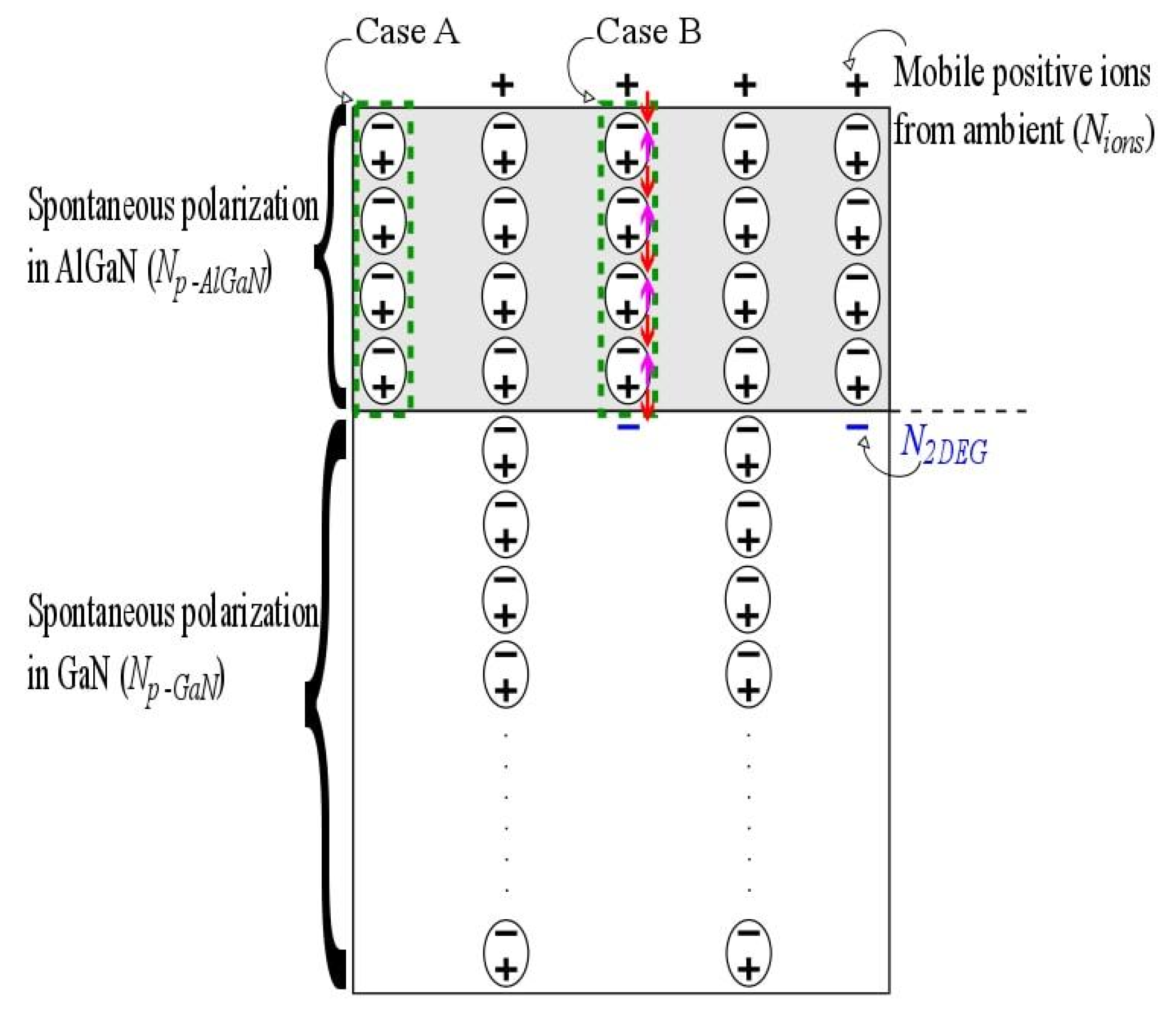
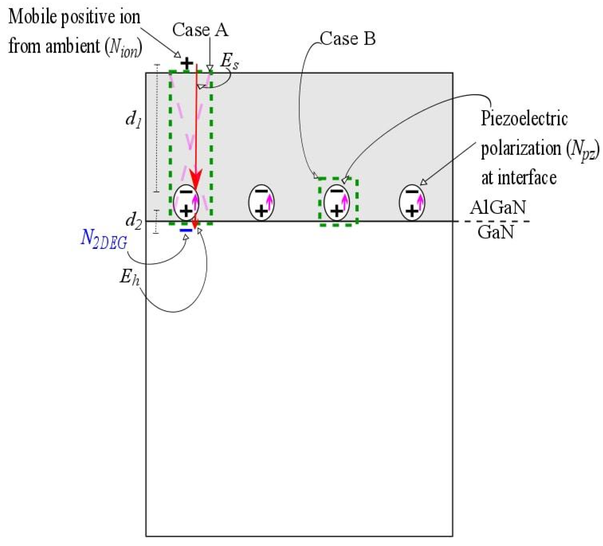
- (1)
- AlGaN surface is unpassivated and accessible by free ions from the ambient;
- (2)
- Metal gate is deposited on the AlGaN surface;
- (3)
- The AlGaN surface is passivated by a thick dielectric layer.
2. Equations for 2DEG in AlGan/GaN Heterostructures
2.1. Unpassivated AlGaN Surface Accessible to Free Ions from Air
2.2. Metal Gate Deposited on AlGaN Surface
2.3. Thick Passivating Dielectric on AlGaN Surface
3. Comparison with Other Models
4. Conclusions
Author Contributions
Funding
Data Availability Statement
Acknowledgments
Conflicts of Interest
References
- Yu, E.T.; Sullivan, G.J.; Asbeck, P.M.; Wang, C.D.; Qiao, D.; Lau, S.S. Measurement of piezoelectrically induced charge in GaN/AlGaN heterostructure field-effect transistors. Appl. Phys. Lett. 1997, 71, 2794–2796. [Google Scholar] [CrossRef] [Green Version]
- Mishra, U.K.; Shen, L.; Kazior, T.E.; Wu, Y.-F. GaN-based RF power devices and amplifiers. Proc. IEEE 2008, 96, 287–305. [Google Scholar] [CrossRef]
- Lee, B.H.; Kim, R.H.; Lim, B.O.; Choi, G.W.; Kim, H.J.; Hong, I.P.; Lee, J.H. High RF performance improvement using surface passivation technique of AlGaN/GaN HEMTs at K-band application. Electron. Lett. 2013, 49, 1013–1015. [Google Scholar] [CrossRef]
- Hanawa, H.; Satoh, Y.; Horio, K. Effects of buffer leakage current on breakdown characteristics in AlGaN/GaN HEMTs with a high-k passivation layer. Microelectron. Eng. 2015, 147, 96–99. [Google Scholar] [CrossRef]
- Yu, C.-H.; Luo, Q.-Z.; Luo, X.-D.; Liu, P.-S. Donor-like surface traps on two-dimensional electron gas and current collapse of AlGaN/GaN HEMTs. Sci. World J. 2013, 2013, 931980. [Google Scholar] [CrossRef] [Green Version]
- Jang, H.W.; Jeon, C.M.; Kim, K.H.; Kim, J.K.; Bae, S.-B.; Lee, J.-H.; Choi, J.W.; Lee, J.-L. Mechanism of two-dimensional electron gas formation in AlxGa1-xN/GaN heterostructures. Appl. Phys. Lett. 2002, 81, 1249–1251. [Google Scholar] [CrossRef] [Green Version]
- Miller, E.J.; Yu, E.T.; Poblenz, C.; Elsass, C.; Speck, J.S. Direct measurement of the polarization charge in AlGaN/GaN heterostructures using capacitance–voltage carrier profiling. Appl. Phys. Lett. 2002, 80, 3551–3553. [Google Scholar] [CrossRef]
- Ramanan, N.; Lee, B.; Kirkpatrick, C.; Suri, R.; Misra, V. Properties of atomic layer deposited dielectrics for AlGaN/GaN device passivation. Semicond. Sci. Technol. 2013, 28, 074004. [Google Scholar] [CrossRef]
- Xiao-Guang, H.; De-Gang, Z.; De-Sheng, J. Formation of two-dimensional electron gas at AlGaN/GaN heterostructure and the derivation of its sheet density expression. Chin. Phys. B 2015, 24, 067301. [Google Scholar]
- Ibbetson, J.P.; Fini, P.T.; Ness, K.D.; DenBaars, S.P.; Speck, J.S.; Mishra, U.K. Polarization effects, surface states, and the source of electrons in AlGaN/GaN heterostructure field effect transistors. Appl. Phys. Lett. 2000, 77, 250–252. [Google Scholar] [CrossRef]
- Morkoc, H. Nitride Semiconductor Devices: Fundamentals and Applications; John Wiley & Sons: Weinheim, Germany, 2013; pp. 31–51. [Google Scholar]
- Ambacher, O.; Foutz, B.; Smart, J.; Shealy, J.R.; Weimann, N.G.; Chu, K.; Murphy, M.; Sierakowski, A.J.; Schaff, W.J.; Eastman, L.F.; et al. Two dimensional electron gases induced by spontaneous and piezoelectric polarization in undoped and doped AlGaN/GaN heterostructures. J. Appl. Phys. 2000, 87, 334–344. [Google Scholar] [CrossRef]
- Ambacher, O.; Smart, J.; Shealy, J.R.; Weimann, N.G.; Chu, K.; Murphy, M.; Schaff, W.J.; Eastman, L.F.; Dimitrov, R.; Wittmer, L.; et al. Two-dimensional electron gases induced by spontaneous and piezoelectric polarization charges in N-and Ga-face AlGaN/GaN heterostructures. J. Appl. Phys. 1999, 85, 3222–3233. [Google Scholar] [CrossRef] [Green Version]
- Dimitrijev, S. Principles of Semiconductor Devices, 2nd ed.; Oxford University Press: New York, NY, USA, 2012; pp. 252–290. [Google Scholar]
- Bhattacharya, D.K.; Sharma, R. Solid State Electronic Devices, 2nd ed.; Oxford University Press: New Delhi, India, 2013; pp. 318–362. [Google Scholar]
- Koley, G.; Spencer, M. On the origin of the two-dimensional electron gas at the Al Ga N/Ga N heterostructure interface. Appl. Phys. Lett. 2005, 86, 042107. [Google Scholar] [CrossRef]
- Higashiwaki, M.; Chowdhury, S.; Miao, M.-S.; Swenson, B.L.; van de Walle, C.G.; Mishra, U.K. Distribution of donor states on etched surface of AlGaN/GaN heterostructures. J. Appl. Phys. 2010, 108, 063719. [Google Scholar] [CrossRef] [Green Version]
- Gordon, L.; Miao, M.-S.; Chowdhury, S.; Higashiwaki, M.; Mishra, U.K.; van de Walle, C.G. Distributed surface donor states and the two-dimensional electron gas at AlGaN/GaN heterojunctions. J. Phys. D 2010, 43, 505501. [Google Scholar] [CrossRef]
- Shealy, J.; Prunty, T.; Chumbes, E.; Ridley, B. Growth and passivation of AlGaN/GaN heterostructures. J. Cryst. Growth 2003, 250, 7–13. [Google Scholar] [CrossRef]
- Maeda, N. Systematic study of insulator deposition effect (Si3N4, SiO2, AlN, and Al2O3) on electrical properties in AlGaN/GaN heterostructures. Jpn. J. Appl. Phys. 2007, 46, 547. [Google Scholar] [CrossRef]
Publisher’s Note: MDPI stays neutral with regard to jurisdictional claims in published maps and institutional affiliations. |
© 2021 by the authors. Licensee MDPI, Basel, Switzerland. This article is an open access article distributed under the terms and conditions of the Creative Commons Attribution (CC BY) license (https://creativecommons.org/licenses/by/4.0/).
Share and Cite
Rathore, S.U.; Dimitrijev, S.; Amini Moghadam, H.; Mohd-Yasin, F. Equations for the Electron Density of the Two-Dimensional Electron Gas in Realistic AlGaN/GaN Heterostructures. Nanomanufacturing 2021, 1, 171-175. https://doi.org/10.3390/nanomanufacturing1030012
Rathore SU, Dimitrijev S, Amini Moghadam H, Mohd-Yasin F. Equations for the Electron Density of the Two-Dimensional Electron Gas in Realistic AlGaN/GaN Heterostructures. Nanomanufacturing. 2021; 1(3):171-175. https://doi.org/10.3390/nanomanufacturing1030012
Chicago/Turabian StyleRathore, Saad Ullah, Sima Dimitrijev, Hamid Amini Moghadam, and Faisal Mohd-Yasin. 2021. "Equations for the Electron Density of the Two-Dimensional Electron Gas in Realistic AlGaN/GaN Heterostructures" Nanomanufacturing 1, no. 3: 171-175. https://doi.org/10.3390/nanomanufacturing1030012
APA StyleRathore, S. U., Dimitrijev, S., Amini Moghadam, H., & Mohd-Yasin, F. (2021). Equations for the Electron Density of the Two-Dimensional Electron Gas in Realistic AlGaN/GaN Heterostructures. Nanomanufacturing, 1(3), 171-175. https://doi.org/10.3390/nanomanufacturing1030012