Article

PVD-Assisted CVD Synthesis of High-Quality Monolayer MoS2: Single Crystals and Centimeter-Scale Films


School of Optometry, Tianjin Vocational University, Tianjin 300410, China
*
Author to whom correspondence should be addressed.
Solids 2026, 7(3), 31; https://doi.org/10.3390/solids7030031
Submission received: 20 April 2026 / Revised: 4 June 2026 / Accepted: 4 June 2026 / Published: 5 June 2026

Abstract

Two-dimensional molybdenum disulfide (MoS2) has emerged as a promising candidate for next-generation electronics and optoelectronics; however, its scalable synthesis with precise control over domain size and film continuity remains challenging. Herein, we report a physical vapor deposition (PVD)-assisted chemical vapor deposition (CVD) strategy for the controllable growth of high-quality monolayer MoS2. By thermally evaporating an ultrathin (3 nm) MoO3 precursor film, spontaneous post-deposition dewetting yields a porous honeycomb morphology that significantly enhances vapor–solid reaction kinetics during subsequent sulfurization. Crucially, by modulating the argon carrier gas flow rate to regulate the local sulfur chemical potential, we achieve distinct growth regimes: a high flow rate (70 sccm) suppresses nucleation density, enabling isolated triangular and hexagonal single crystals with lateral dimensions up to 500 μm, whereas a reduced flow rate (50 sccm) promotes high-density nucleation and coalescence into continuous centimeter-scale polycrystalline films. Comprehensive structural and optical characterizations, including atomic force microscopy, Raman spectroscopy, photoluminescence, and X-ray photoelectron spectroscopy, confirm that the synthesized MoS2 exhibits prototypical monolayer thickness (~0.7 nm), well-defined local crystallinity and a direct bandgap emission at 1.84 eV. This work establishes a robust, scalable, and highly tunable route for synthesizing large-area 2D TMDs tailored for advanced device integration.

Graphical Abstract

1. Introduction

Since the discovery of graphene in 2004, the study of two-dimensional (2D) materials has expanded to include many other layered crystals [1]. Two-dimensional transition metal dichalcogenides (TMDs) have emerged as one of the most promising candidate materials for investigating electrical properties, owing to their unique electronic structures and distinctive physical characteristics [1,2,3]. The primary motivation for preparing 2D TMDs, particularly MoS2, lies in their thickness-dependent electronic properties. Unlike bulk MoS2 which possesses an indirect bandgap, the monolayer form exhibits a direct bandgap. This transition effectively addresses the lack of a natural bandgap in graphene, making it highly suitable for transistors and optoelectronic devices. In addition, monolayer MoS2 presents novel physical phenomena such as strong excitonic effects and valleytronic properties [1]. Among various bottom-up synthesis approaches for two dimensional materials, physical vapor deposition (PVD) [4,5] and chemical vapor deposition (CVD) [6,7,8] represent the two techniques with the greatest potential for industrial-scale development. To realize these applications, chemical vapor deposition has established itself as a prevalent growth method for controlling the morphology of two-dimensional TMDs, offering considerable advantages including simplified equipment requirements, reduced manufacturing costs, and enhanced process flexibility [9].
Physical vapor deposition constitutes an effective methodology for fabricating large-scale, ultrathin TMD films, characterized by elevated growth rates and substantial material diversity [10]. Through pre-deposition of metal or oxide thin films via PVD techniques such as electron beam evaporation [11,12], resistive thermal evaporation [13], and magnetron sputtering [14] followed by direct sulfurization of the as-deposited precursor films, TMDs can be synthesized on diverse substrates in a scalable and controllable manner [15,16,17,18]. Nevertheless, this deposition method offers opportunities for further optimization. Transition metal oxide thin films deposited by PVD tend to possess a relatively high density, which may lead to a correspondingly higher nucleation site density during the subsequent sulfurization process. Under such conditions, the lateral growth of two-dimensional crystals along the substrate surface may be somewhat constrained, resulting in smaller crystalline domains and non-uniform thickness in the final two-dimensional materials. These factors indicate that there remains room for improvement in terms of the uniformity of two-dimensional films, the size of single crystalline domains, deposition reproducibility, process stability, and overall material scalability.
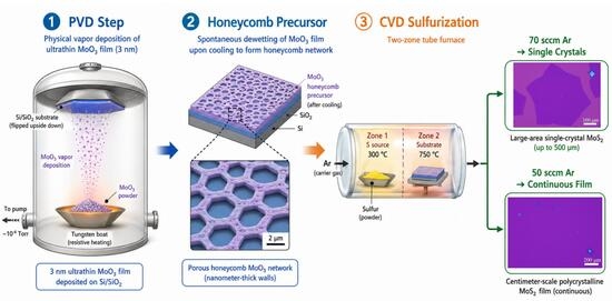
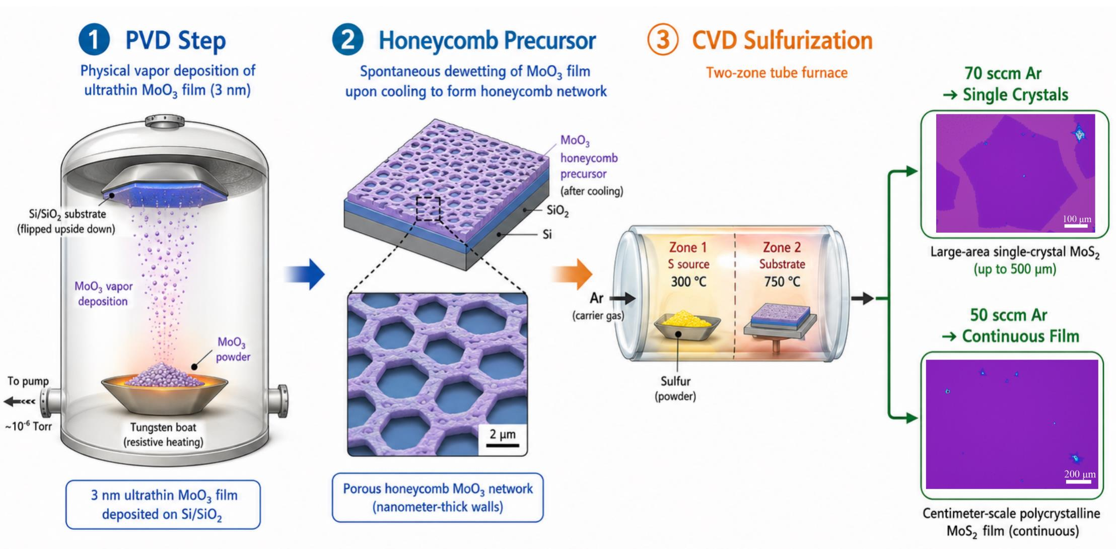
To circumvent these limitations, we herein develop a two-step PVD-assisted CVD methodology that decouples precursor deposition from sulfurization kinetics. By thermally evaporating an ultrathin (3 nm) MoO3 film, we exploit the inherent solid state dewetting of sub-critical thickness films to spontaneously generate a porous, honeycomb-like precursor morphology upon cooling. This discontinuous network substantially increases the interfacial area available for vapor solid reactions, thereby promoting complete and uniform sulfurization compared to conventional dense or powdered precursors. Furthermore, we demonstrate that the sulfur chemical potential and consequently the nucleation and lateral growth dynamics can be precisely tuned by modulating the carrier gas flow rate in a two-zone tube furnace. Under optimized conditions, this approach enables the deterministic synthesis of either isolated single crystalline domains with lateral sizes up to 500 μm or continuous, centimeter-scale polycrystalline monolayer films. This study provides a versatile, scalable, and highly reproducible pathway for tailoring the morphology and domain architecture of 2D MoS2 for advanced optoelectronic applications.

2. Materials and Methods

During the experimental preparation stage, the Si/SiO2 substrates were pretreated as follows: they were first rinsed three times with ethanol, acetone, and deionized water, respectively, and then transferred to a vacuum drying oven and treated at 75 °C for 1 h until use. To prevent contamination during the thermal evaporation process, the surface of the tungsten boat was polished smooth with sandpaper to remove the oxide layer, followed by ultrasonic cleaning with deionized water and drying in a vacuum drying oven for later use.
The preparation of MoO3 thin films is shown in Figure 1a: The sample powders were placed in a tungsten boat (20 mg of MoO3, 99.995% purity). The tungsten boat was then placed in the heating stage inside the vacuum chamber. The pressure in the coating machine chamber was reduced to 1 × 10⁻⁵ Torr using a mechanical pump and a molecular pump, followed by the thermal evaporation experiment. Initially, a shutter was placed between the powder and the Si/SiO2 substrate to block impurities, and then the heating current was increased at a rate of 0.05 A/min, causing a rapid rise in the temperature of the heating stage. The deposition rate and thickness of the powder were monitored using a film-thickness monitor. For MoO3, when the current was increased to 0.8 A, the MoO3 powder began to sublime due to heating and deposit onto the Si/SiO2 substrate surface. When the current reached 1.2 A, the MoO3 powder sublimated at a constant rate. The deposition rate was maintained at approximately 0.1 nm/s. At this point, the shutter was opened, and the sublimated powder deposited onto the Si/SiO2 substrates placed upside down at a distance of approximately 15 cm above the top of the vacuum chamber, resulting in a final thickness of 3 nm.
Figure 1b shows the scanning electron microscopy (SEM) image of the MoO3 thin film. We observe that the film exhibits a honeycomb structure. This is due to the low thickness of the film; after evaporation, as the sample cools, the film undergoes spontaneous agglomeration. However, this irregular and porous film structure is beneficial because, compared to powder precursors and dense film precursors, it greatly increases the collision probability between transition metal oxide molecules and with other reactants, thereby allowing the reaction to proceed more completely.
Figure 1c is a schematic diagram of the experimental setup for growing two-dimensional TMDs using the two-step PVD-assisted CVD method. The Si/SiO2 substrate with the deposited precursor film is loaded onto a quartz boat, which is placed at the center of the high-temperature reaction zone (750 °C). Then, sulfur powder (50 mg, 99.995% purity) is placed in a low-temperature zone (300 °C) located 20 cm upstream of the quartz boat. Before heating, the furnace is evacuated to 80 mTorr and then backfilled with Ar gas (99.999% purity) to atmospheric pressure. This cleaning cycle is repeated 3–5 times, and then the entire CVD system is purged with Ar gas at a flow rate of 500 sccm for 20 min to remove water molecules and oxygen from the chamber. Subsequently, the Ar flow rate was reduced to 70 (single crystal) or 50 (thin film) sccm and maintained at this value throughout the growth process as the carrier gas. The heating rate for both the precursor zone and the sulfur zone was set to 50 °C/min. The system is then heated to the desired temperature for the reaction. The precursor zone reached 750 °C and the sulfur zone reached 300 °C. The growth was maintained at these temperatures for 15 min. The specific growth conditions and parameters for each material are listed in Table 1. When the growth is terminated, an Ar flow of 500 sccm is introduced into the furnace to remove residual reactants, while the furnace is pushed out of the hot zone to rapidly cool the sample to room temperature with an estimated cooling rate of ~100 °C/min (the sample cooled from 750 °C to room temperature within approximately 8–10 min).
During the initial stage of the CVD reaction process, the nanometer-thick precursor film absorbs thermal energy. The molecules in the film undergo thermal motion, and due to their thermally induced vibrations in all directions, the integrity of the precursor film is disrupted, allowing sulfur to chemically react with these transition metal oxide molecules. Compared to powdered transition metal oxide precursors, this precursor uniformly spread on the substrate surface is more favorable for the full growth of crystals. Ultimately, high-quality, large-size two-dimensional transition metal dichalcogenides are obtained.

3. Results and Discussion

Unlike previously reported dense MoO3 precursor films obtained by sputtering or e-beam evaporation [19,20], the 3 nm MoO3 film deposited by thermal evaporation in this work undergoes spontaneous agglomeration during post-deposition cooling, resulting in a porous honeycomb morphology. This randomly distributed porous structure substantially enhances the collision probability between MoO3 and sulfur vapor enabling three-dimensional vapor permeation rather than diffusion-limited solid-phase reaction, thereby facilitating more complete sulfurization and yielding monolayer MoS2 with well-defined local crystallinity with domain sizes up to 500 μm and centimeter-scale continuous films, in stark contrast to the nanocrystalline few-layer MoS2 obtained from dense precursor films.
This morphology arises from a well-established phenomenon in thin-film physics. The spontaneously formed porous honeycomb morphology can be understood in the framework of solid state dewetting of ultrathin films [21,22]. For films below a critical thickness on SiO2 substrates [23,24], surface energy minimization drives hole nucleation at grain boundaries via grooving [25], followed by hole growth and edge retraction, ultimately resulting in a discontinuous porous network [26]. Similar agglomeration behavior has been observed in thermally evaporated thin films [27], including molybdenum oxide films [28,29].
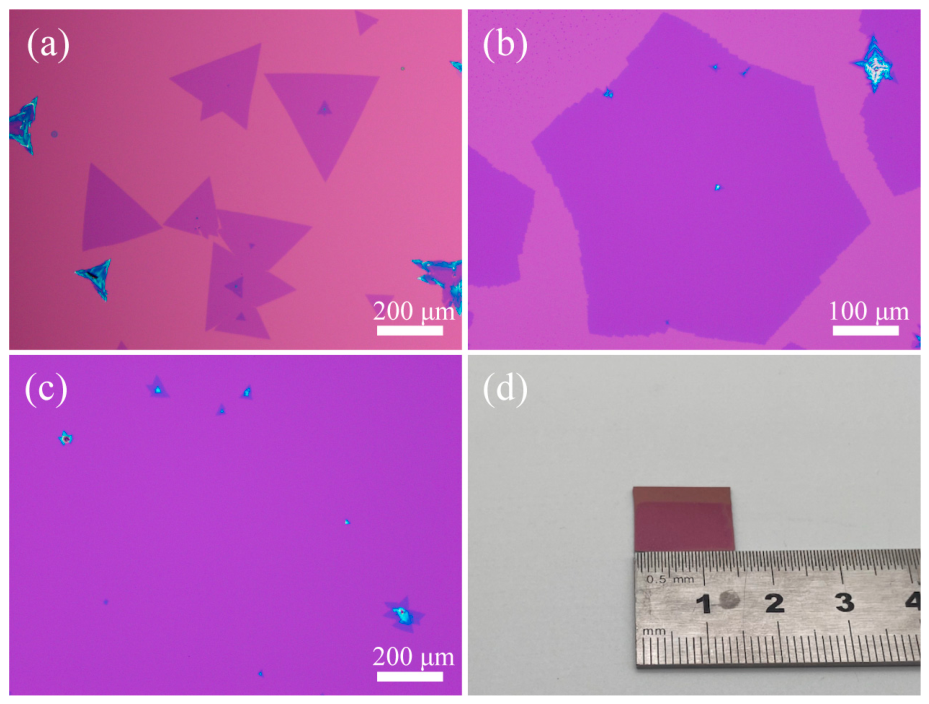
Figure 2a,b show the two-dimensional MoS2 crystals grown by the PVD-assisted CVD technique. It can be observed that under a relatively high carrier gas flow rate (70 sccm), the sample shapes are triangular and hexagonal. From Figure 2c, it can be seen that under a lower carrier gas flow rate (50 sccm), the sample morphology is a continuous crystalline film. Figure 2d shows an overall photograph of the film. In the two-zone furnace configuration employed here, the carrier gas flow rate governs the residence time of sulfur vapor over the MoO3 precursor film [30]. Under a low carrier gas flow rate (50 sccm), prolonged residence time results in a high local concentration of sulfur species at the growth interface, corresponding to a high supersaturation condition. High supersaturation lowers the nucleation barrier, thereby promoting a high density of nucleation events [31,32]. As growth proceeds, the closely spaced nuclei rapidly expand and impinge upon one another, ultimately coalescing into a continuous polycrystalline monolayer film with a lateral extent reaching the centimeter scale (1.5 cm). Conversely, under a high carrier gas flow rate (70 sccm), the shorter residence time of sulfur vapor yields a lower supersaturation at the growth front. The correspondingly higher nucleation barrier suppresses excessive nucleation, resulting in a sparse distribution of nuclei with ample inter-nucleus spacing. Each nucleus can therefore undergo sustained lateral growth without impingement, giving rise to isolated triangular and hexagonal single crystals with lateral dimensions exceeding 200 μm for triangles and reaching up to 500 μm for hexagons. This competition between nucleation density and lateral growth space governed by the sulfur chemical potential modulated through carrier gas flow is consistent with the established kinetic framework for CVD growth of 2D TMDs [33,34]. MoO3 sulfurization using dense precursor films deposited by sputtering or atomic layer deposition typically yields few-layer (2–3 layers) MoS2 with nanocrystalline domains at growth temperatures of 800–1000 °C [19,20]; conventional powder-based CVD under comparable thermal conditions, on the other hand, generally produces isolated monolayer flakes with lateral dimensions on the order of tens of micrometers [33]. By contrast, the PVD-assisted CVD method reported here achieves strictly monolayer MoS2 at a lower temperature and offers the additional capability to form centimeter-scale continuous films through straightforward carrier gas flow modulation.
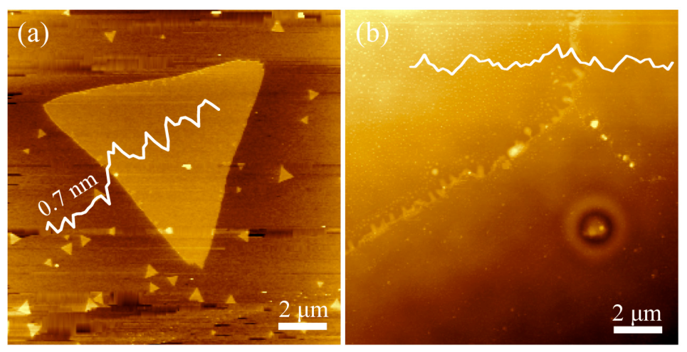
Figure 3a shows the AFM measurement results of a triangular sample. The thickness of the single domain is approximately 0.7 nm, which is consistent with the typical thickness (0.6–0.7 nm) of mechanically exfoliated monolayer materials [35]. During the CVD process, the sublimated sulfur vapor reacts with the reduced molybdenum species derived from MoO3 to nucleate and grow MoS2 on the substrate. As established by Rajan et al. [36], sulfur acts as the limiting reagent in this reaction, and its concentration gradient along the reactor directly controls both the crystal shape and growth rate. Under sulfur rich or sulfur deficient conditions, the Mo-zigzag and S-zigzag edges grow at disparate rates, yielding triangular domains, while a balanced Mo/S stoichiometry produces hexagonal shapes. The well-faceted triangular morphology observed in our sample indicates that sulfur was the dominant limiting reagent under our growth conditions, consistent with a kinetically limited growth regime. Figure 3b shows that at the domain boundaries of the polycrystalline film, there are no particle attachments or oxide layers, indicating that the as-grown two-dimensional MoS2 product is of high quality.
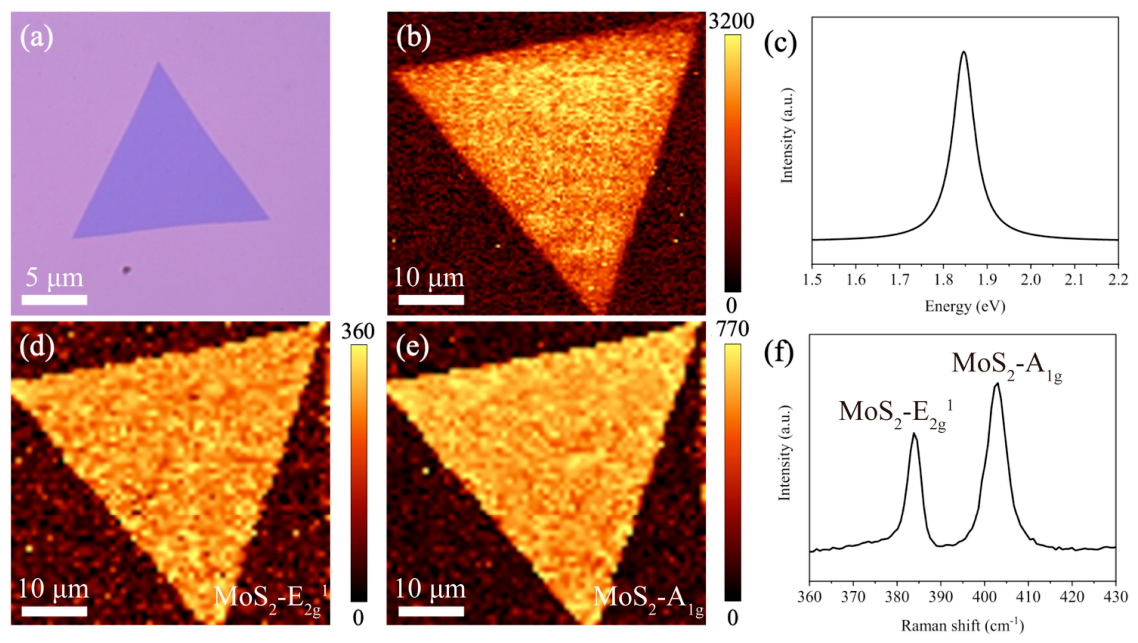
The as-grown MoS2 was characterized by Raman and photoluminescence (PL) spectroscopy using a 532 nm excitation source. Figure 4a shows an optical image of a representative triangular MoS2 flake. Figure 4b,c present the PL intensity mapping and the corresponding spectrum acquired from the flake center. A dominant emission peak centered at 1.84 eV is observed, corresponding to the A-exciton transition characteristic of the direct bandgap in monolayer MoS2 [37]. Notably, the peak exhibits a full width at half maximum (FWHM) of approximately 69 meV. This narrow linewidth comparable to high-quality mechanically exfoliated samples indicates a low density of defects and trap states, confirming the high optical quality of the CVD-grown film. The PL mapping reveals a uniform intensity distribution across the flake center, further demonstrating the spatial homogeneity of the monolayer [38].
Figure 4d–f display the Raman characterization of the same region. The spectrum reveals two primary vibrational modes: the in-plane E2g1 mode at 383.8 cm−1 and the out-of-plane A1g mode at 403.0 cm−1. The frequency difference (Δ) between these modes is calculated to be 19.2 cm−1. This value serves as a definitive fingerprint for monolayer thickness, as it is distinct from the larger separation (~25 cm−1) typically observed in bulk MoS2 crystals [39]. Furthermore, a detailed analysis of the peak positions provides insight into the film’s strain and doping status. The E2g1 mode is sensitive to lattice strain, while the A1g mode responds to carrier doping. The observed positions, slightly red-shifted compared to strain-free suspended flakes, suggest the presence of mild biaxial tensile strain induced by the thermal expansion mismatch with the SiO2/Si substrate during the cooling process, a common feature in CVD grown 2D films. Combined, the PL and Raman analyses confirm that the as grown MoS2 is a high-quality, monolayer semiconductor with uniform structural and optical properties.
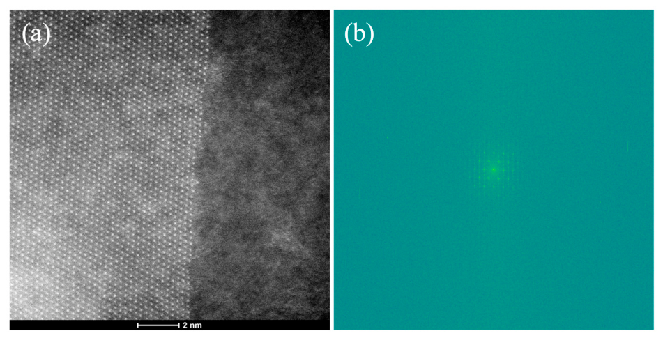
To further verify the crystallinity and structural quality of the film, we performed atomic-resolution scanning transmission electron microscopy (STEM). As shown in Figure 5a, the HR-STEM image clearly resolves the atomic lattice with well-defined periodicity. A measured lattice spacing of approximately 0.27 nm is observed, which corresponds to the (100) plane spacing of MoS2. The image also reveals a sharp interface between the crystalline domain (left) and the amorphous region (right), confirming the localized growth of the film on the substrate. The crystalline nature of the observed lattice is further corroborated by the Fast Fourier Transform (FFT) analysis of the selected area, as presented in Figure 5b. The FFT pattern displays distinct diffraction spots arranged in a hexagonal symmetry, which is characteristic of the hexagonal lattice structure of MoS2. Although slight distortion in the diffraction spots is observed, likely due to local lattice strain or sample tilt during transfer, the presence of sharp, well-defined peaks provides strong evidence of the sample’s local crystalline quality, ruling out the possibility of amorphous growth.
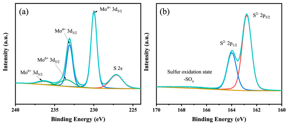
High-resolution XPS spectra were analyzed using CASAXPS software to reveal the surface chemical composition and valence states of the sample. Peak fitting was performed using a mixed Gaussian–Lorentzian line shape (LA(1643)), with strict physical constraints applied: spin–orbit splitting energies (ΔBE) and doublet area ratios were fixed to their theoretical values throughout the analysis. The Mo 3d spectrum (Figure 6a) exhibits a pair of intense peaks at 229.32 eV and 232.42 eV, attributed to the Mo4+ 3d5/2 and 3d3/2 orbitals, respectively, characteristic of molybdenum in the MoS2 lattice, with a spin–orbit splitting energy of 3.10 eV. Additionally, a pair of weak peaks observed at 232.50 eV and 235.60 eV are assigned to Mo6+ (3d5/2 and 3d3/2). The presence of Mo6+ is typically ascribed to slight surface oxidation upon air exposure or sulfur vacancies at the lattice edges. Based on peak area integration, the proportion of Mo6+ is negligible (<10%), indicating that the bulk of the sample remains in a well-reduced state.
The S 2p spectrum (Figure 6b) shows a doublet at 162.79 eV and 163.98 eV corresponding to S2− 2p3/2 and 2p1/2, with a peak separation of 1.19 eV and an area ratio close to 2:1, consistent with the theoretical constraint. Based on the integrated peak areas, the surface Mo:S atomic ratio is calculated to be approximately 1:2.03, which is in close agreement with the ideal stoichiometric ratio of MoS2 (1:2), suggesting that the synthesized product possesses high phase purity.

4. Conclusions

In summary, we have demonstrated a highly tunable PVD-assisted CVD strategy for the controllable synthesis of monolayer MoS2 with tailored morphologies and domain architectures. The key innovation lies in leveraging the spontaneous solid state dewetting of an ultrathin (3 nm) thermally evaporated MoO3 film, which yields a porous honeycomb precursor that significantly enhances sulfurization efficiency and ensures stoichiometric conversion. By precisely modulating the carrier gas flow rate to govern the local sulfur chemical potential, we successfully navigated the competition between nucleation density and lateral expansion. This kinetic control enables the deterministic growth of isolated single crystals with lateral dimensions up to 500 μm under high-flow conditions (70 sccm), or continuous, centimeter-scale polycrystalline films under low-flow conditions (50 sccm). Extensive characterization via AFM, Raman, PL, and XPS confirms that both growth regimes yield high-quality monolayer MoS2 with a thickness of ~0.7 nm, a direct bandgap emission at 1.84 eV, and exceptional phase purity. This approach offers a promising pathway toward scalable synthesis of 2D TMDs.

Author Contributions

Conceptualization, H.Y.; methodology, H.Y.; software, H.Y.; validation, H.Y. and X.F.; formal analysis, H.Y.; investigation, H.Y.; resources, H.Y.; data curation, H.Y.; writing—original draft, H.Y.; writing—review and editing, H.Y. and X.F.; visualization, H.Y.; supervision, H.Y.; project administration, H.Y. and X.F.; funding acquisition, H.Y. and X.F. All authors have read and agreed to the published version of the manuscript.

Funding

This research was funded by Tianjin Municipal Education Commission’s Scientific Research Plan Project of 2023 (2023KJ283, X.W. Fan).

Data Availability Statement

Data are contained within the article.

Conflicts of Interest

The authors declare no conflicts of interest.

References

  1. Luo, Y.; Zhao, J.; Fieramosca, A.; Guo, Q.; Kang, H.; Liu, X.; Liew, T.C.H.; Sanvitto, D.; An, Z.; Ghosh, S.; et al. Strong light-matter coupling in van der Waals materials. Light Sci. Appl. 2024, 13, 203. [Google Scholar] [CrossRef] [Scilit]
  2. Fan, X.; Xin, R.; Li, L.; Zhang, B.; Li, C.; Zhou, X.; Chen, H.; Zhang, H.; OuYang, F.; Zhou, Y. Progress in the preparation and physical properties of two-dimensional Cr-based chalcogenide materials and heterojunctions. Front. Phys. 2024, 19, 23401. [Google Scholar] [CrossRef] [Scilit]
  3. Zou, T.; Kim, S.; Reo, Y.; Heo, S.; Liu, A.; Noh, Y.Y. Electrical properties of electrochemically exfoliated 2D transition metal dichalcogenides transistors for complementary metal-oxide-semiconductor electronics. Adv. Electron. Mater. 2024, 10, 2300691. [Google Scholar] [CrossRef] [Scilit]
  4. Thodkar, K.; Plodinec, M.; Gramm, F.; Kunze, K. Probing the intrinsic strain in suspended graphene films using electron and optical microscopy. Adv. Sci. 2024, 11, 2305366. [Google Scholar] [CrossRef] [Scilit] [PubMed]
  5. Madoune, Y.; Yang, D.; Ahmed, Y.; Al-Makeen, M.M.; Huang, H. PVD growth of spiral pyramid-shaped WS2 on SiO2/Si driven by screw dislocations. Front. Chem. 2023, 11, 1132567. [Google Scholar] [CrossRef] [Scilit] [PubMed]
  6. Yuan, Y.; Weber, J.; Li, J.; Tian, B.; Ma, Y.; Zhang, X.; Taniguchi, T.; Watanabe, K.; Lanza, M. On the quality of commercial chemical vapour deposited hexagonal boron nitride. Nat. Commun. 2024, 15, 4518. [Google Scholar] [CrossRef] [Scilit]
  7. Wan, Z.; Wang, C.; Zheng, H.; Tang, W.; Fu, Z.; Liu, W.; Zhou, Z.; Li, J.; Yuan, G.; Gao, L. Fabrication of two-dimensional van der Waals moiré superlattices. Chin. Phys. B 2025, 34, 047302. [Google Scholar] [CrossRef] [Scilit]
  8. Sagar, R.U.R.; Khan, U.; Galluzzi, M.; Aslam, S.; Nairan, A.; Anwar, T.; Ahmad, W.; Zhang, M.; Liang, T. Transfer-Free Growth of Bi2O2Se on Silicon Dioxide via Chemical Vapor Deposition. ACS Appl. Electron. Mater. 2020, 2, 2123–2131. [Google Scholar] [CrossRef] [Scilit]
  9. Bizhani, M.; Jensen, G.; Poston, W.; Aldosari, N.; Tariq, M.; Aleithan, S.; Stinaff, E. Selective oxidation of metallic contacts for localized chemical vapor deposition growth of 2D-transition metal dichalcogenides. Mater. Res. Express 2024, 11, 015901. [Google Scholar] [CrossRef] [Scilit]
  10. Saikia, R.; Kakati, B.; Hazarika, T.; Sharma, S.; Rajbongshi, T.; Das, M.; Biswas, S.; Kundu, S.; Mahanta, M.K. Fabrication of Microcrystalline Silicon Thin Film by Ionized Physical Vapor Deposition Process. Crystals 2025, 15, 106. [Google Scholar] [CrossRef] [Scilit]
  11. Sivakumar, R.; Gopalakrishnan, R.; Jayachandran, M.; Sanjeeviraja, C. Characterization on electron beam evaporated α-MoO3 thin films by the influence of substrate temperature. Curr. Appl. Phys. 2007, 7, 51–59. [Google Scholar] [CrossRef] [Scilit]
  12. Sun, X.; Zhao, H.; Chen, J.; Zhong, W.; Zhu, B.; Tao, L. Effects of the thickness and laser irradiation on the electrical properties of e-beam evaporated 2D bismuth. Nanoscale 2021, 13, 2648–2657. [Google Scholar] [CrossRef] [Scilit]
  13. Park, J.Y.; Kim, H.K. Flexible Metal/Oxide/Metal Transparent Electrodes Made of Thermally Evaporated MoO3/Ag/MoO3 for Thin Film Heaters. Phys. Status Solidi A 2018, 215, 1800674. [Google Scholar] [CrossRef] [Scilit]
  14. Nirupama, V.; Chandra Sekhar, M.; Subramanyam, T.K.; Uthanna, S. Structural and electrical characterization of magnetron sputtered MoO3 thin films. J. Phys. Conf. Ser. 2010, 208, 012101. [Google Scholar] [CrossRef] [Scilit]
  15. Liu, H.; Ansah Antwi, K.K.; Ying, J.; Chua, S.; Chi, D. Towards large area and continuous MoS2 atomic layers via vapor-phase growth: Thermal vapor sulfurization. Nanotechnology 2014, 25, 405702. [Google Scholar] [CrossRef] [Scilit]
  16. Yang, K.Y.; Nguyen, H.T.; Tsao, Y.M.; Artemkina, S.B.; Fedorov, V.E.; Huang, C.W.; Wang, H.C. Large area MoS2 thin film growth by direct sulfurization. Sci. Rep. 2023, 13, 8378. [Google Scholar] [CrossRef] [Scilit]
  17. Kumar, P.; Singh, M.; Sharma, R.K.; Reddy, G.B. Role of different ambient on sulfurization of MoO3 into MoS2. J. Alloys Compd. 2016, 671, 440–445. [Google Scholar] [CrossRef] [Scilit]
  18. Tsai, H.S.; Huang, Y.H.; Tsai, P.C.; Chen, Y.J.; Ahn, H.; Lin, S.Y.; Lu, Y.J. Ultrafast exciton dynamics in scalable monolayer MoS2 synthesized by metal sulfurization. ACS Omega 2020, 5, 10725–10730. [Google Scholar] [CrossRef] [Scilit] [PubMed]
  19. Panasci, S.E.; Koos, A.; Schilirò, E.; Di Franco, S.; Greco, G.; Fiorenza, P.; Roccaforte, F.; Agnello, S.; Cannas, M.; Gelardi, F.M.; et al. Multiscale Investigation of the Structural, Electrical and Photoluminescence Properties of MoS2 Obtained by MoO3 Sulfurization. Nanomaterials 2022, 12, 182. [Google Scholar] [CrossRef] [Scilit]
  20. Romanov, R.I.; Kozodaev, M.G.; Myakota, D.I.; Chernikova, A.G.; Novikov, S.M.; Volkov, V.S.; Slavich, A.S.; Zarubin, S.S.; Chizhov, P.S.; Khakimov, R.R.; et al. Synthesis of Large Area Two-Dimensional MoS2 Films by Sulfurization of Atomic Layer Deposited MoO3 Thin Film for Nanoelectronic Applications. ACS Appl. Nano Mater. 2019, 2, 7521–7531. [Google Scholar] [CrossRef] [Scilit]
  21. Thompson, C.V. Solid-State Dewetting of Thin Films. Annu. Rev. Mater. Res. 2012, 42, 399–434. [Google Scholar] [CrossRef] [Scilit]
  22. Danielson, D.T.; Sparacin, D.K.; Michel, J.; Kimerling, L.C. Surface-Energy-Driven Dewetting Theory of Silicon-on-Insulator Agglomeration. J. Appl. Phys. 2006, 100, 083507. [Google Scholar] [CrossRef] [Scilit]
  23. Boragno, C.; Buatier de Mongeot, F.; Felici, R.; Robinson, I.K. Critical Thickness for the Agglomeration of Thin Metal Films. Phys. Rev. B 2009, 79, 155443. [Google Scholar] [CrossRef] [Scilit]
  24. Gadkari, P.R.; Warren, A.P.; Todi, R.M.; Petrova, R.V.; Coffey, K.R. Comparison of the Agglomeration Behavior of Thin Metallic Films on SiO2. J. Vac. Sci. Technol. A Vac. Surf. Film. 2005, 23, 1152–1161. [Google Scholar] [CrossRef] [Scilit]
  25. Amram, D.; Klinger, L.; Gazit, N.; Gluska, H.; Rabkin, E. Grain Boundary Grooving in Thin Films Revisited: The Role of Interface Diffusion. Acta Mater. 2014, 69, 386–396. [Google Scholar] [CrossRef] [Scilit]
  26. Jacquet, P.; Podor, R.; Ravaux, J.; Lautru, J.; Teisseire, J.; Gozhyk, I.; Jupille, J.; Lazzari, R. On the Solid-State Dewetting of Polycrystalline Thin Films: Capillary Versus Grain Growth Approach. Acta Mater. 2018, 143, 281–290. [Google Scholar] [CrossRef] [Scilit]
  27. Sharma, S.K.; Rao, S.U.M.; Kumar, N. Hillock Formation and Agglomeration in Silver Films Prepared by Thermal Evaporation. Thin Solid Films 1986, 142, L95–L98. [Google Scholar] [CrossRef] [Scilit]
  28. Arfaoui, A.; Touihri, S.; Mhamdi, A.; Labidi, A.; Manoubi, T. Structural, Morphological, Gas Sensing and Photocatalytic Characterization of MoO3 and WO3 Thin Films Prepared by the Thermal Vacuum Evaporation Technique. Appl. Surf. Sci. 2015, 357, 1089–1096. [Google Scholar] [CrossRef] [Scilit]
  29. Borah, D.J.; Mostako, A.T.T.; Saikia, P.K.; Dutta, P. Effect of Thickness and Post Deposition Annealing Temperature on the Structural and Optical Properties of Thermally Evaporated Molybdenum Oxide Films. Mater. Sci. Semicond. Process. 2019, 93, 111–122. [Google Scholar] [CrossRef] [Scilit]
  30. Bai, M.; Wen, S.; Zhao, J.; Du, Y.; Xie, F.; Liu, H. Effect of Carrier Gas Flow Field on Chemical Vapor Deposition of 2D MoS2 Crystal. Coatings 2021, 11, 547. [Google Scholar] [CrossRef] [Scilit]
  31. Zhou, D.; Shu, H.; Hu, C.; Jiang, L.; Liang, P.; Chen, X. Unveiling the Growth Mechanism of MoS2 with Chemical Vapor Deposition: From Two-Dimensional Planar Nucleation to Self-Seeding Nucleation. Cryst. Growth Des. 2018, 18, 1012–1019. [Google Scholar] [CrossRef] [Scilit]
  32. Kumar, V.K.; Rathkanthiwar, S.; Rao, A.; Ghosh, P.; Dhar, S.; Chandrasekar, H.; Choudhury, T.; Shivashankar, S.A.; Raghavan, S. Role of Surface Processes in Growth of Monolayer MoS2: Implications for Field-Effect Transistors. ACS Appl. Nano Mater. 2021, 4, 7138–7148. [Google Scholar] [CrossRef] [Scilit]
  33. Xu, H.; Zhou, W.; Zheng, X.; Huang, J.; Feng, X.; Ye, L.; Xu, G.; Lin, F. Control of the Nucleation Density of Molybdenum Disulfide in Large-Scale Synthesis Using Chemical Vapor Deposition. Materials 2018, 11, 870. [Google Scholar] [CrossRef] [Scilit]
  34. Yang, S.Y.; Shim, G.W.; Seo, S.B.; Choi, S.Y. Effective Shape-Controlled Growth of Monolayer MoS2 Flakes by Powder-Based Chemical Vapor Deposition. Nano Res. 2017, 10, 255–262. [Google Scholar] [CrossRef] [Scilit]
  35. Li, H.; Wu, J.; Yin, Z.; Zhang, H. Preparation and Applications of Mechanically Exfoliated Single-Layer and Multilayer MoS2 and WSe2 Nanosheets. Acc. Chem. Res. 2014, 47, 1067–1075. [Google Scholar] [CrossRef] [Scilit] [PubMed]
  36. Rajan, A.G.; Warner, J.H.; Blankschtein, D.; Strano, M.S. Generalized Mechanistic Model for the Chemical Vapor Deposition of 2D Transition Metal Dichalcogenide Monolayers. ACS Nano 2016, 10, 4330–4344. [Google Scholar] [CrossRef] [Scilit]
  37. Radisavljevic, B.; Radenovic, A.; Brivio, J.; Giacometti, V.; Kis, A. Single-layer MoS2 transistors. Nat. Nanotechnol. 2011, 6, 147–150. [Google Scholar] [CrossRef] [Scilit]
  38. Chiu, M.H.; Zhang, C.; Shiu, H.W.; Chuu, C.P.; Chen, C.H.; Chang, C.Y.S.; Chen, C.H.; Chou, M.Y.; Shih, C.K.; Li, L.J. Determination of band alignment in the single-layer MoS2/WSe2 heterojunction. Nat. Commun. 2015, 6, 7666. [Google Scholar] [CrossRef] [Scilit] [PubMed]
  39. Lee, C.; Yan, H.; Brus, L.E.; Heinz, T.F.; Hone, J.; Ryu, S. Anomalous Lattice Vibrations of Single- and Few-Layer MoS2. ACS Nano 2010, 4, 2695–2700. [Google Scholar] [CrossRef] [Scilit]
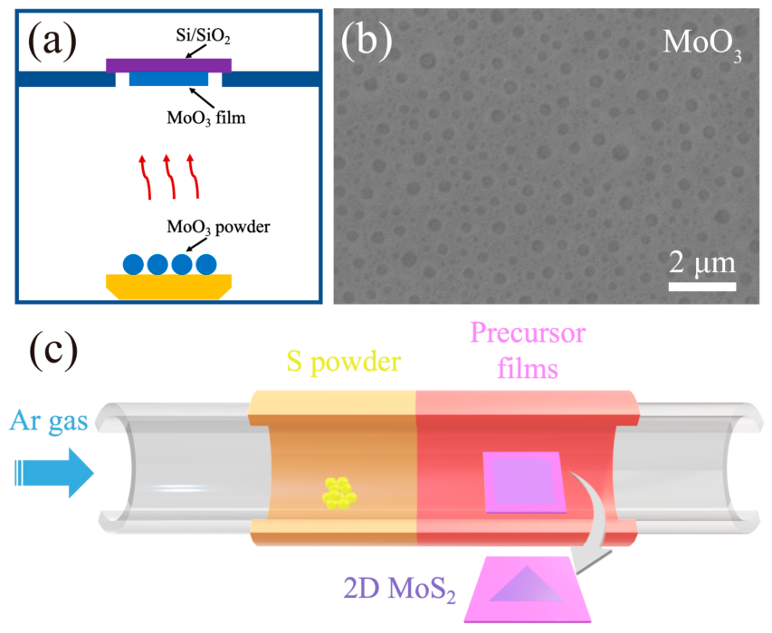
Figure 1. (a) Schematic illustrations for films by physical vapor deposition (PVD) method. (b) Scanning electron microscope images (SEM) for MoO3. (c) Schematic diagram for CVD growth equipment for 2D TMDs.
Solids 07 00031 g001
Figure 2. Optical image of 2D MoS2: (a) triangle, (b) hexagon, (c) large size film and (d) photo of film.
Solids 07 00031 g002
Figure 3. AFM image of 2D MoS2: (a) triangle single crystal, (b) crystal domain boundary of large-scale thin film.
Solids 07 00031 g003
Figure 4. Raman and PL characterization of 2D MoS2 single crystals. (a) Optical image. (b) PL intensity mapping at 1.84 eV, corresponding to the characteristic PL peak of MoS2. (c) The PL spectrum collected at the center of the crystal domain shows the PL characteristic peak of monolayer MoS2. (d) and (e) Raman intensity mapping at 383.8 cm−1 and 403 cm−1, showing triangular-shaped crystal domains. (f) The Raman spectrum collected at the center of the crystal domain shows the Raman characteristic peak of monolayer MoS2.
Solids 07 00031 g004
Figure 5. (a) High-resolution STEM image of the atomic structure. Periodic lattice fringes (left) indicate a crystalline domain, while the amorphous region (right) corresponds to the substrate. Scale bar: 2 nm. (b) STEM image corresponding FFT.
Solids 07 00031 g005
Figure 6. XPS spectrum of 2D MoS2. The binding energy of (a) Mo 3d and S 2s and (b) S 2p.
Solids 07 00031 g006
Table 1. Growth conditions and parameters of 2D TMDs.
MaterialPrecursor Film Thickness (nm)Growth Temperature (°C)Carrier Gas Flow Rate (Sccm)
MoS2 single crystalMoO3
(3 nm)
750Ar
(70 sccm)
MoS2 thin filmMoO3
(3 nm)
750Ar
(50 sccm)
Disclaimer/Publisher’s Note: The statements, opinions and data contained in all publications are solely those of the individual author(s) and contributor(s) and not of MDPI and/or the editor(s). MDPI and/or the editor(s) disclaim responsibility for any injury to people or property resulting from any ideas, methods, instructions or products referred to in the content.