Abstract
This study explores the feasibility of using Cu/AZO thin films as low-emissivity materials with antibacterial properties, fabricated using the linear sputtering method. The linear sputtering technique deposits thin films onto continuous substrates, offering high throughput, uniform coatings, and precise control over film properties. In this research, Cu/AZO thin films underwent either vacuum annealing or hydrogen plasma annealing treatments. The Cu layer imparts antibacterial properties, while the AZO layer primarily provides thermal insulation. Experimental results show that annealing treatments enhance both photoelectric performance and antibacterial capability. Annealed Cu/AZO films exhibit lower resistivity and emissivity. Among the samples, those subjected to vacuum annealing at 400 °C are most suitable for low-emissivity applications, with an average visible light transmittance of 60%, an emissivity of 0.16, and an antibacterial activity value of 8.8. The Cu/AZO films proposed in this study effectively combine antibacterial and thermal insulation properties, making them relevant for the field of green materials.
1. Introduction
Low emissivity glass, or low-E glass, is a type of low-emissivity material that features high transmittance in the visible light spectrum and high reflectance in the infrared spectrum. The use of low-E glass in buildings allows for excellent indoor lighting while providing effective thermal insulation, making it a popular material in modern green building construction. It is highly regarded in discussions of green building and energy issues [1,2,3]. Among commercially available low-E glass products, the emissivity is a crucial factor for consumers when selecting low-E glass. A lower emissivity value indicates better thermal insulation performance.
The structure of low-emissivity glass typically involves multilayer thin films based on metals or metal thin films that are transparent in the visible light spectrum [4,5,6]. For instance, multilayer thin films based on metals often use silver due to its excellent visible light transmittance and infrared reflectance. However, silver is prone to oxidation and has poor adhesion properties. Therefore, to enhance optical performance, provide oxidation resistance, and improve adhesion, seed layers and barrier layers are often added, creating what is known as a silver-based single-layer film structure.
To effectively improve the optical performance of low-E glass, such as infrared reflectance and visible light transmittance, silver-based single-layer films are typically stacked to form silver-based multilayer film structures. This multilayer approach can result in film layers exceeding nine layers. While this method enhances the optical performance of the glass, it also increases production costs and time.
Public facilities (such as municipal buildings and healthcare institutions) and transportation vehicles (like buses and subways) extensively use glass materials. In hospitals, glass surfaces often come into contact with patients and medical staff. If the glass can provide sterilization and thermal insulation, it would contribute to a safe, well-lit, and comfortable environment in patient rooms. In public transportation, glass surfaces that passengers frequently touch would greatly benefit from antibacterial properties to help prevent the spread of germs. Thus, antibacterial glass represents a crucial application for both healthcare and public transportation settings.
Currently, many researchers are focusing on the antibacterial applications of metals, particularly due to the excellent antibacterial properties of copper and copper alloys [7,8,9,10]. Copper can maintain its antibacterial activity as long as the alloy contains 60% or more copper. Researchers have already explored the use of metallic copper as an antibacterial or antimicrobial material in medical facilities such as hospitals. For instance, J.V. Prado and colleagues studied the adhesion of bacteria commonly found in hospitals on samples of copper and stainless steel. Their study found that copper samples adhered to fewer bacteria, while bacteria on stainless steel samples increased rapidly [10].
The use of metals such as copper and silver for antibacterial purposes has a long history. It is generally believed that cell death is caused by multiple factors rather than a single, universal mechanism [11]. According to literature, the toxic effects of copper arise from the alteration between the oxidation states of Cu+ and Cu2+, providing electrons. This allows copper to act as a catalyst for the generation of reactive oxygen species (ROS), such as hydroxyl radicals and superoxide anions. ROS can damage essential cellular components like proteins, nucleic acids, and lipids [12,13]. Additionally, free copper ions may compete with zinc or other metal ions for critical binding sites on proteins, leading to conformational changes and loss of protein function [14].
Recent research on the antibacterial mechanisms of copper has highlighted one such mechanism called contact killing. This involves studying the effects of microorganisms exposed to copper surfaces and how copper reduces microbial populations. Contact killing refers to the process by which copper ions disrupt cell membranes, generate oxygen-containing free radicals, and damage cellular DNA, leading to cell death.
Emissivity is a crucial reference indicator for low-emissivity glass, with lower emissivity values indicating better thermal insulation performance. According to the Hagen-Rubens relation [15], emissivity is closely related to resistivity; as resistivity decreases, emissivity also decreases. Consequently, many scholars have recently explored the feasibility of using materials such as indium tin oxide (ITO) and aluminum-doped zinc oxide (AZO) in low-emissivity glass [16,17,18].
In 2020, T. Horiuchi and K. Yoshimura noted that ITO contains the toxic element indium and suggested using AZO as an alternative material for low-emissivity glass [18]. They further investigated the solar heat gain coefficient (SHGC) of AZO when used in low-emissivity glass. Our research team has also reported on the effects of plasma annealing on the structure, electrical, and optical properties of AZO/ITO thin films [19,20]. Previous reports indicate that the duration of vacuum annealing and hydrogen plasma annealing treatments impacts the structure of AZO/ITO thin films, thereby reducing resistivity and improving electrical performance [19].
Additionally, our team studied the effects of plasma annealing under different H2/N2 gas ratios on AZO/ITO thin films [20]. We found that an appropriate H2/N2 gas ratio during plasma annealing can reduce the resistivity of AZO/ITO thin films by 58%, which in turn lowers the emissivity.
If low-emissivity materials can provide antibacterial and thermal insulation functions, they can create a safe, well-lit, and comfortable environment. This is particularly important in public transportation, where passengers frequently touch glass surfaces. Antibacterial properties in such glass can help prevent the spread of germs. Therefore, this study proposes a method for preparing Cu/AZO thin films using the linear continuous sputtering technique for application on glass. The linear continuous sputtering system offers advantages such as high production throughput. Finally, the structure, electrical, optical, low-emissivity, and antibacterial properties of the Cu/AZO thin films were measured.
2. Experiments
First, borosilicate glass substrates were cleaned sequentially using acetone, deionized water, and isopropanol in an ultrasonic cleaner for 5 min each. After cleaning, the substrates were dried with nitrogen gas to remove moisture. Following the cleaning process, aluminum-doped zinc oxide (AZO) and copper (Cu) thin films were deposited onto the glass substrates using a linear continuous sputtering system, as illustrated in Figure 1. The total thickness of the thin films was 510 nm, with the Cu layer and the AZO layer being 10 nm and 500 nm thick, respectively.

Figure 1.
Schematic diagram of prepared test piece.
Initially, the AZO thin film was deposited onto the glass substrate using the linear continuous sputtering system. The AZO target (ZnO = 98.5%:1.5 wt.%) was sputtered under conditions of 2500 W DC power, 250 sccm Ar flow rate, and 3 mTorr working pressure. Subsequently, the Cu layer was deposited onto the partially deposited AZO thin film using the same sputtering system. The Cu target (99.9% wt.%) was sputtered under conditions of 1000 W DC power, 250 sccm Ar flow rate, and 3 mTorr working pressure. The prepared samples underwent either vacuum annealing or hydrogen plasma annealing treatments.
The vacuum annealing treatment was performed at a pressure of 10−5 Torr, with the Cu/AZO thin films annealed at temperatures of 300 °C and 400 °C for 1 h. For the hydrogen plasma annealing treatment, the Cu/AZO thin films were annealed for 5 min at gas flow rates of 100 sccm, gas pressure of 25 Torr, and varying powers of 400 W and 600 W.
The samples, both before and after annealing treatments, were analyzed using various characterization techniques. The crystal structure of the thin films was observed using X-ray diffraction (XRD; Bruker D2 Phaser, Bruker AXS GmbH, Karlsruhe, Germany). The surface microstructure was examined with a scanning electron microscope (SEM; HITACHI SU8000, HITACHI, Japan). Electrical properties, including resistivity, carrier concentration, and mobility, were measured using a Hall measurement system (Ecopia HMS-3000, Ecopia, Gyeonggi-do, Republic of Korea). Optical transmittance in the 400–800 nm range was measured with a UV/VIS spectrophotometer (Hitachi U-2800A, Hitachi, Tokyo, Japan). The emissivity of the Cu/AZO films was determined using an emissivity meter (TSS-5X, Japan Sensor, Tokyo, Japan). Finally, the antibacterial efficacy of the Cu/AZO films against Escherichia coli ATCC 8739 (E. coli) was evaluated according to the JIS Z 2801:2010 standard [21].
3. Results and Discussion
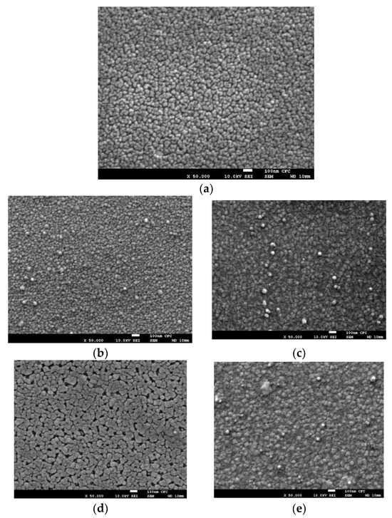
The surface morphology of the Cu/AZO thin films, both before and after annealing treatments, was observed using SEM, as shown in Figure 2a–e. The SEM images of the Cu/AZO samples are shown as follows: (a) represents the unannealed sample, (b) and (c) are vacuum-annealed samples at temperatures of 300 °C and 400 °C, respectively, and (d) and (e) are hydrogen plasma-annealed samples with plasma powers of 400 W and 600 W, respectively. The grain shape and size of the unannealed Cu/AZO thin films were similar to those of the samples vacuum-annealed at 300 °C (Figure 2b). As the vacuum annealing temperature increased to 400 °C, agglomeration began to occur shown in Figure 2c. This suggests that the thermal energy at 400 °C is sufficient to trigger agglomeration. Figure 2d,e show the micrographs of the Cu/AZO thin films after hydrogen plasma annealing. It was observed that more pronounced agglomeration occurred in the Cu/AZO thin films after hydrogen plasma annealing compared to vacuum annealing. This suggests that hydrogen plasma annealing transfers more energy to the samples than vacuum annealing.

Figure 2.
SEM photos of Cu/AZO specimens (a) is unannealed, (b,c) are vacuum annealed at temperatures of 300 and 400 degrees respectively, (d,e) are hydrogen plasma annealed processing, plasma power is 400 W and 600 W respectively.
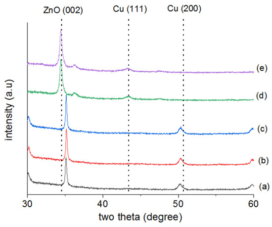
Figure 3 shows the XRD measurements of the crystal phases of Cu/AZO thin films prepared under various conditions. The XRD spectra of Cu/AZO films fabricated using different methods (unannealed, vacuum annealed, and hydrogen plasma annealed) are shown. (a) represents the unannealed sample, (b) and (c) are the vacuum annealed samples at temperatures of 300 °C and 400 °C, respectively, and (d) and (e) are the hydrogen plasma annealed samples with plasma powers of 400 W and 600 W, respectively. The XRD spectra were measured at diffraction angles ranging from 30° to 60°. For all Cu/AZO thin films, the (002) peak corresponding to the ZnO crystal plane, as identified by ICDD PDF card number 36-1451, was observed. Additionally, the (111) and (200) peaks corresponding to the Cu crystal plane were also observed.

Figure 3.
XRD spectra of Cu/AZO produced using different methods (unannealed, vacuum annealed and hydrogen plasma annealed). (a) is not annealed, (b) and (c) are vacuum annealed, the temperatures are 300 and 400 degrees respectively, (d) and (e) are hydrogen plasma annealed, the plasma power is 400 W and 600 W respectively.
As shown in Figure 3, the Cu(200) peak, as indicated by ICDD PDF card number 04-0836, and the ZnO(002) peak of the unannealed Cu/AZO thin films shift to higher angles after vacuum annealing. The shift in XRD diffraction peaks to lower or higher angles may be due to changes in the interplanar spacing. The shift of the ZnO(002) peak to a higher angle indicates a reduction in interplanar spacing, which might be related to aluminum ions substituting for zinc ions in the AZO lattice.
For the Cu/AZO thin films subjected to hydrogen plasma annealing, the Cu(200) peak was not observed; instead, the Cu(111) crystal plane was detected, suggesting a phase transformation of Cu. Additionally, in the hydrogen plasma-annealed samples, the ZnO(002) peak shifted to lower angles, indicating an increase in interplanar spacing.
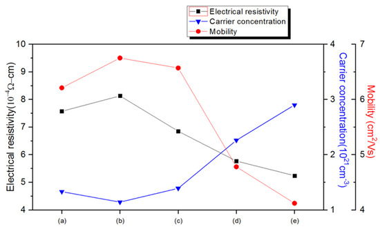
The electrical properties of Cu/AZO thin films after vacuum annealing and hydrogen plasma annealing are shown in Figure 4 and Table 1. As observed in Figure 4, the resistivity of the Cu/AZO thin film increased after vacuum annealing at 300 °C. However, as the annealing temperature increased to 400 °C, the resistivity decreased. The resistivity did not decrease at 300 °C possibly because the temperature was not high enough. Figure 2a,b show that the surface of the Cu/AZO thin films was similar before and after vacuum annealing at 300 °C.

Figure 4.
The electrical properties of Cu/AZO films fabricated using different annealing methods (unannealed, vacuum annealed, and hydrogen plasma annealed) are presented, including carrier concentration, mobility, and resistivity. (a) represents the unannealed sample, (b) and (c) are the vacuum annealed samples at temperatures of 300 °C and 400 °C, respectively, and (d) and (e) are the hydrogen plasma annealed samples with plasma powers of 400 W and 600 W, respectively.

Table 1.
Electrical, emissivity, optical and antibacterial activity properties of Cu/AZO films prepared using various annealing methods. (a) Unannealed; (b) Vacuum annealed at 300 °C; (c) Vacuum annealed at 400 °C; (d) Hydrogen plasma annealed at 400 W; (e) Hydrogen plasma annealed at 600 W.
The decrease in resistivity at 400 °C could be attributed to the provided thermal energy being sufficient for aluminum ions to substitute zinc ions in the AZO lattice. This substitution provides free electrons, thereby increasing the carrier concentration. After hydrogen plasma annealing, the resistivity of the Cu/AZO thin films showed a significant decreasing trend. The resistivity of the unannealed Cu/AZO thin film was 7.57 × 10⁻⁴ Ω-cm. After hydrogen plasma annealing at 600 W, the resistivity decreased to a minimum value of 5.24 × 10⁻⁴ Ω-cm, which is a 30% reduction compared to the unannealed Cu/AZO thin film.
This reduction in resistivity could be due to hydrogen atoms acting as shallow donors when Cu/AZO is treated with H2 plasma. According to Liu et al., hydrogen atoms diffuse into the AZO thin film and occupy the Zn-O bond center. This diffusion might increase the interplanar spacing in the Cu/AZO thin films, as indicated by the shift of the (002) peak to a lower angle in Figure 3 after H2 plasma treatment. The increase in point defects within the film may lower the mobility of the material, while also increasing the carrier concentration due to these defects.
The emissivity of the Cu/AZO thin films before and after annealing treatments is recorded in Table 1. As shown in Table 1, the emissivity of the Cu/Al-doped ZnO thin films decreased after hydrogen plasma annealing. Comparing the resistivity and emissivity from Table 1, it is evident that lower resistivity correlates with lower emissivity. According to the Hagen-Rubens relationship, the resistivity of a material is closely related to its emissivity; as resistivity decreases, emissivity also decreases. Indeed, this study observed a simultaneous reduction in resistivity and emissivity.
For the unannealed Cu/AZO thin film, the emissivity was 0.18. After hydrogen plasma treatment (600 W), the emissivity decreased to 0.13, which is a 27% reduction compared to the unannealed sample.
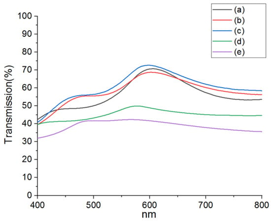
The visible light transmittance spectra (400~800 nm) of Cu/AZO films prepared under various conditions were analyzed using a UV/VIS spectrophotometer, as shown in Figure 5. Table 1 also presents the average visible light transmittance for Cu/AZO films, including those treated with hydrogen plasma (400 W, 600 W) and vacuum annealing (300 °C and 400 °C). From Figure 5 and Table 1, it can be observed that the visible light transmittance of the untreated and vacuum-annealed samples is relatively similar. In contrast, the visible light transmittance of the hydrogen plasma-treated samples is significantly reduced, which may be associated with phase transformations of Cu in the samples, as indicated by the XRD results in Figure 3. Further investigation is needed to clarify this effect in future studies.

Figure 5.
The visible light transmittance spectra of Cu/AZO films prepared using different methods (untreated, vacuum annealed, and hydrogen plasma annealed). (a) represents the untreated sample, (b) and (c) represent the vacuum-annealed samples at 300 °C and 400 °C, respectively, and (d) and (e) represent the hydrogen plasma-annealed samples at 400 W and 600 W, respectively.
Antibacterial testing was conducted according to the Japanese Industrial Standard JIS Z 2801:2000, using Escherichia coli (ATCC 8739) for the antibacterial tests. According to the JIS Z 2801:2000 standard, products with an antibacterial activity value (R) greater than 2.0 are classified as meeting the “effective” antibacterial product standards. The antibacterial effect of the samples was measured at one time point (24 h) and is shown in the antibacterial activity column of Table 1. The Cu/AZO samples, whether untreated, vacuum annealed, or hydrogen plasma annealed, all exhibited antibacterial activity values greater than 7. Meanwhile, the single-layer AZO’s antibacterial activity was measured, yielding an R value of 0.8. The untreated Cu/AZO samples had high antibacterial activity, and vacuum annealing further increased the antibacterial activity, while hydrogen plasma annealing decreased the R value. This may be explained by the contact killing mechanism, where microorganisms in contact with the Cu surface are killed through the release of copper ions, which disrupt cell membranes, generate reactive oxygen species, and ultimately damage the cell DNA.
4. Conclusions
In this study, Cu/AZO thin films were fabricated using a linear sputtering method, and their feasibility as low-emissivity materials was explored. Additionally, the Cu/AZO thin films underwent vacuum annealing or hydrogen plasma annealing treatments. The Cu/AZO structure not only provides antibacterial properties through the Cu layer but also offers thermal insulation capabilities, with the AZO layer contributing to the insulating effect. The experimental results indicate that the annealed Cu/AZO films exhibited lower resistivity and emissivity. The most suitable Cu/AZO sample for low-emissivity applications was found to be the one treated with vacuum annealing at 400 °C, achieving an average visible light transmittance of 60%, an emissivity of 0.16, and an antibacterial activity value of 8.8. The Cu/AZO films proposed in this study demonstrate both antibacterial and thermal insulation functions, suggesting their potential application in the field of green materials in the future.
Author Contributions
Conceptualization, investigation, funding acquisition, project administration and methodology, S.-C.C.; validation, formal analysis, writing—review and editing, S.-C.C. and J.-S.W.; resources, J.-S.W. All authors have read and agreed to the published version of the manuscript.
Funding
This research was funded by the National Science and Technology Commission of Taiwan for financial support under contract no. NSTC 112-2637-E-168-002.
Institutional Review Board Statement
Not applicable.
Informed Consent Statement
Not applicable.
Data Availability Statement
The original contributions presented in the study are included in the article, further inquiries can be directed to the corresponding author.
Acknowledgments
This work was partially supported by the Green Energy Technology Research Center of Kunshan University.
Conflicts of Interest
The authors declare no conflicts of interest.
References
- KiranKumar, G.; Saboor, S.; Babu, T.P.A. Investigation of Various Low Emissivity Glass Materials for Green Energy Building Construction in Indian Climatic Zones. Mater. Today Proc. 2017, 4, 8052–8058. [Google Scholar] [CrossRef]
- Lee, S.Y. Low Emissivity Property of Amorphous Oxide Multilayer (SIZO/Ag/SIZO) Structure. Trans. Electr. Electron. Mater. 2017, 18, 13–15. [Google Scholar] [CrossRef][Green Version]
- Baetens, R.; Jelle, B.P.; Gustavsen, A. Properties, requirements and possibilities of smart windows for dynamic daylight and solar energy control in buildings: A state-of-the-art review. Sol. Energy Mater. Sol. Cells 2010, 94, 87–105. [Google Scholar] [CrossRef]
- Karlsson, B.; Valkonen, E.; Karlsson, T.; Ribbing, C.-G. Materials for solar-transmitting heat-reflecting coatings. Thin Solid Film. 1981, 86, 91–98. [Google Scholar] [CrossRef]
- Ding, G.; Clavero, C. Silver-Based Low-Emissivity Coating Technology for Energy-Saving Window Applications. In Modern Technologies for Creating the Thin-Film Systems and Coatings; Nikitenkov, N.N., Ed.; IntechOpen: Rijeka, Croatia, 2017; Chapter 20. [Google Scholar]
- Jelle, B.P.; Kalnæs, S.E.; Gao, T. Low-emissivity materials for building applications: A state-of-the-art review and future research perspectives. Energy Build. 2015, 96, 329–356. [Google Scholar] [CrossRef]
- HansSalima, M. Physicochemical properties of copper important for its antibacterial activity and development of a unified model. Biointerphases 2016, 11, 018902. [Google Scholar]
- Rtimi, S.; Dionysiou, D.D.; Pillai, S.C.; Kiwi, J. Advances in catalytic/photocatalytic bacterial inactivation by nano Ag and Cu coated surfaces and medical devices. Appl. Catal. B Environ. 2019, 240, 291–318. [Google Scholar] [CrossRef]
- Ondok, V.; Musil, J.; Meissner, M.; Čerstvý, R.; Fajfrlík, K. Two-functional DC sputtered Cu-containing TiO2 thin films. J. Photochem. Photobiol. A: Chem. 2010, 209, 158–162. [Google Scholar] [CrossRef]
- Prado, J.V.; Esparza, M.M.; Vidal, A.R. Adherence to copper and stainless steel metal coupons of common nosocomial bacterial strains. Rev. Méd. Chile 2013, 141, 291–297. [Google Scholar]
- Warnes, S.L.; Caves, V.; Keevil, C.W. Mechanism of copper surface toxicity in Escherichia coli O157:H7 and Salmonella involves immediate membrane depolarization followed by slower rate of DNA destruction which differs from that observed for Gram-positive bacteria. Environ. Microbiol. 2012, 14, 1730–1743. [Google Scholar] [CrossRef] [PubMed]
- Espírito-Santo, C.; Lam, E.W.; Elowsky, C.G.; Quaranta, D.; Domaille, D.W.; Chang, C.J.; Grass, G. Bacterial killing by dry metallic surfaces. Appl. Environ. Microbiol. 2011, 77, 794–802. [Google Scholar] [CrossRef] [PubMed]
- Warnes, S.; Keevil, C. Mechanism of copper surface toxicity in vancomycin-resistant enterococci following wet or dry surface contact. Appl. Environ. Microbiol. 2011, 77, 6049–6059. [Google Scholar] [CrossRef] [PubMed]
- Borkow, G.; Gabbay, J. Copper, an ancient remedy returning to fight microbial, fungal and viral infections. Curr. Chem. Biol. 2009, 3, 272–278. [Google Scholar]
- Hagen, E.; Rubens, H. Über Beziehungen des Reflexions-und Emissionsvermögens der Metalle zu ihrem elektrischen Leitvermögen. Ann. Phys. 1903, 316, 873–901. [Google Scholar] [CrossRef]
- Garlisi, C.; Trepci, E.; Li, X.; Al, R.; Al-ali, K.; Pereira, R.; Zheng, L.; Azar, E.; Palmisano, G. Multilayer thin film structures for multifunctional glass: Self-cleaning, antireflective and energy-saving properties. Appl. Energy 2020, 264, 114697. [Google Scholar] [CrossRef]
- Miller, M.J.; Wang, J. Multilayer ITO/VO2/TiO2 thin films for control of solar and thermal spectra. Sol. Energy Mater. Sol. Cells 2016, 154, 88–93. [Google Scholar] [CrossRef]
- Horiuchi, T.; Yoshimura, K. Solar heat gain coefficient and heat transmission coefficient of Al-doped ZnO thin-film coated low-emissivity glass. J. Ceram. Soc. Jpn. 2020, 128, 220–223. [Google Scholar] [CrossRef]
- Chang, S.C.; Chan, H.T. Post-annealed Aluminum-Doped Zinc Oxide/Tin-Doped Indium Oxide Bilayer Films for Low Emissivity Glass. Int. J. Electrochem. Sci. 2020, 15, 3694–3703. [Google Scholar] [CrossRef]
- Chang, S.-C.; Chan, H.-T. Effect of Nitrogen Flow in Hydrogen/Nitrogen Plasma Annealing on Aluminum-Doped Zinc Oxide/Tin-Doped Indium Oxide Bilayer Films Applied in Low Emissivity Glass. Crystals 2019, 9, 310. [Google Scholar] [CrossRef]
- JIS Z 2801:2010; Antimicrobial Products—Test for Antimicrobial Activity and Efficacy. Japanese Standards Association: Tokyo, Japan, 2010.
Disclaimer/Publisher’s Note: The statements, opinions and data contained in all publications are solely those of the individual author(s) and contributor(s) and not of MDPI and/or the editor(s). MDPI and/or the editor(s) disclaim responsibility for any injury to people or property resulting from any ideas, methods, instructions or products referred to in the content. |
© 2024 by the authors. Licensee MDPI, Basel, Switzerland. This article is an open access article distributed under the terms and conditions of the Creative Commons Attribution (CC BY) license (https://creativecommons.org/licenses/by/4.0/).