Review

Surface Plasmons Excited by X-rays in the Surface Layers of Solids

by
Valery M. Stozharov
Faculty of Physics, St-Petersburg State Pedagogical University, 191186 St. Petersburg, Russia
Solids 2022, 3(1), 122-146; https://doi.org/10.3390/solids3010009
Submission received: 12 November 2021 / Revised: 10 February 2022 / Accepted: 14 February 2022 / Published: 1 March 2022
(This article belongs to the Special Issue Solids in Europe)

Abstract

:
The phenomenon of total external reflection of X-rays at a sliding angle of incidence of a beam of incident X-rays is investigated. For metals, a quantitative law of direct dependence of the refractive index decrement on the interplane distance is obtained. The excitation of surface plasmons by X-rays that have experienced complete external reflection is detected. For surface plasmons, a dimensional effect was observed, expressed in an increase in the energy of plasmons and the concentration of conduction electrons with an increase in the depth of the output of surface plasmons. By the method of dispersion of surface plasmons, internal mechanical micro-stresses and spontaneous polarization of the surface layers of glassy dielectrics and in thin layers of vanadium dioxide were determined. The absence of micro-stresses in the lithium fluoride ionic single crystal was found out, and the polarization observed in it is due to the large dipole moment of the molecules of this crystal. In thin films of vanadium dioxide, the dependence of micro-stresses on the stresses in the substrates was found.

1. Introduction

Elementary excitations associated with the collective motion of weakly bound valence electrons relative to the crystal lattice of positive ions in solids are plasma longitudinal waves. Quanta of such waves with energy E P = ω are called plasmons [1]. Thus, plasmons are quantized oscillations of collectivized electrons of the valence band of dielectrics and semiconductors and the conduction bands of metals [2].
Depending on the method and conditions of excitation, plasmon are divided into a number of classes, the main of which are bulk and surface plasmon [3]. Thus, the excitation of plasmon by fast kilovolt electrons on the shoting thin films leads to characteristic energy losses of primary electrons on bulk plasmon with energies of the order of 20 eV. The study of the dependence of the elastic reflection of slow electrons with energies from 3 to 25 eV from the surface of alkaline earth metals [4] leads to the excitation of quanta of surface plasmons of low energies of the order of several electron-volts.
In recent decades, a detailed theoretical and experimental study of the optical properties of surface plasmons in insular and ultrafine metallic media has begun [5,6,7]. These studies served as the basis for the creation of an optical surface plasmon a microscope that is currently widely used in biology and medicine [8].
The excitation of plasma oscillations by electromagnetic waves leads to theoretical concepts based on dielectric formalism [1,9]. This is due to the physics of the interaction of electromagnetic waves with a solid, which leads to the polarization of the crystal as a result of the displacement of electrons under the action of an electromagnetic field. The polarization of a solid is known to be characterized by its dielectric constant ε.
Plasma oscillations in a solid can also excite X-rays under the condition of a sliding incidence of an X-ray beam at an angle of several angular minutes, at which the X-ray radiation experiences a total external reflection in thin layers of solids with a thickness of no more than 15 nm. Therefore, in this case, only surface plasmons with energies of several electron volts can be excited. However, the use in our works the spectral line of soft X-ray radiation CuKα1 with a wavelength λ = 1.5406 Å and, accordingly, with a large quantum energy E = hν = 8040 eV, far exceeding the energy of surface plasmons, which should lead to a vanishingly low probability of excitation surface plasmons with such energetic X-ray quanta. This is explained by the quantum mechanical description of microparticles based on the idea of their particle-wave dualism and describing the resonant interaction between microparticles, which becomes probable when their frequencies coincide [10].
This explains the high probability of excitation of surface plasmons in the case of elastic reflection of slow electrons with energies from 3 to 25 eV from alkaline earth metals [4], as well as resonant excitation of surface plasmons by laser radiation in the visible region of the spectrum of electromagnetic waves with an energy of about 5 eV [7,11]. Therefore, the main role in the excitation of surface plasmons by X-rays should also be played by slow electrons with the most probable energy (2–5) eV, entering due to secondary electron amplification in thin surface layers of solids are the composition of multielectronic acts of X-ray photoemission in the form of electronic bundles [12,13]. In [14], the role of slow electrons in the excitation of plasma oscillations in solids by X-rays is considered in detail.
This review, the phenomenon of total external reflection of X-rays from the surface layers of solids is considered in detail. This phenomenon is characterized by arefractive index slightly less than one. The review also explains the effect of double refracion in a number of polycrystalline metals by reflections from different crystallites with different interplane distances. Using the technique of total external reflection of X-rays, the review obtained data onmeasuring the energy of surface plasmons, the depths of the output of plasmons, the number of electrons forming surface plasmons and detected their dimensional effect. In the last part of the review, the dispersion of surface plasmons is considered, determined by the dependence of the energy of plasmons on their wave vector for crystalline and amorphous bodies and thin films. Analyzing dispersion loop-like curves, mechanical microstresses in the surface layers of solids and electronic asymmetry associated with spontaneous polarization of surface layers and thin films are determined.

1.1. Total External Reflection of X-rays from the Surface of Solids

Since the study of the properties of surface plasmons in solids using X-rays possible only under the conditions of their sliding angle of incidence of the X-ray beam on the surface of solids, at which it experiences a total external reflection (TER), the beginning of the review is devoted to a detailed consideration of this phenomenon. The total external reflection of the X-rays from the surface of solids at sliding angles of incidence of the X-ray beam was discovered and investigated back in the 20 s of the last century [15,16]. The main results of these studies were two effects: firstly, the refractive index of X-rays found in solids is less than one and, secondly, the small depths of the formation TER of the X-ray in various substances from units to hundreds of angstroms (Å). The surface character TER of the X-ray, which provides a reflection coefficient close to one, is used in practice to create a paraxial beam with low divergence, on the basis of which X-ray fluorescence analysis with high sensitivity up to 10−10 g [17] and the study of the properties TER of the X-ray [18] is carried out.
In [18], a comprehensive study of X-ray reflection was carried out, including measurements of radiographs TER and X-ray diffraction. For this purpose, a standard DRON-7 diffractometer was used, manufactured at the St. Petersburg industrial enterprise “Burevestnik”, with the minimum possible step in the X-ray scattering angle ∆(2θ) = 0.001° = 3.6′. In front of the output window of an acute-focus X-ray tube with a copper anode, a parabolic mirror is installed, providing paraxiality of the incident X-ray beam with a divergence of about 0.5′ and completely suppressing the spectral line of CuKβ X-ray radiation. A scintillation counter in the mode of counting X-ray quanta with an efficiency of about 100% was used as a detector. In front of the detector there is a collimator and a horizontal Soller slit. In this case, the recording of radiographs TER of X-ray in the 2θ-θ mode ensures that the curve TER of X-ray is obtained with a maximum.
However, in most works on the total external reflection of X-rays from solids, radiographs are integral curves in the form of quasi-step functions, the greatest slope of which corresponds sliding angle α TER of the X-ray, which determines the refractive index of X-rays in solids [15,16,19]. Since in our works radiographs of X-ray differ from the integral ones, a methodical experiment was undertaken on a single crystal of silicon (111) in order to compare the integral curve of TER with the curves of TER with maxima obtained in our work [18]. The integral curve of the TER was obtained without a parabolic mirror, without a collimator and a Soller slit in the “θ” mode, characterized by scanning the sample along the angle θ with a stationary detector. In Figure 1, a comparison of the integral curve of TER with the curve of TER, characterized by a maximum, shows the coincidence of the maximum with the section of the integral curve of TER with the greatest slope. Therefore, TER curves with a maximum can be called differential TER curve.
The differential radiograph of TER for polished tantalum, shown in Figure 2, showed two maxima corresponding to two different refractive indices of X-rays.
For quantitative interpretation of abnormal radiographs TER polished tantalum, shown in Figure 2, we should consider the principles of refraction of X-rays in solids [18]:
1. The position of the maximum on the reflection curves at sliding angles α close to zero uniquely determines the refractive index n of X-rays in solids slightly less than one and is associated with the angle α by a simple ratio of geometric optics:
n = cos   α
2. The decrement δ of the refractive index of X-rays, determined by the formula
δ = 1 n = 1 cos   α  
is always a positive number. According to the quantum mechanical theory of dispersion [20], the decrement δ of the refractive index is proportional to the volume density NV of scattering atoms in accordance with the ratio for a monatomic material:
δ = λ 2 e 2 2 π mc 2 N V Z
where in the international SI system λ = 1.5406 × 10 10 m is the wavelength of the incident X-ray radiation; e = 1.602 × 10⁻¹⁹ Kool is electron charge; m = 9.109 × 10⁻³¹ kg is electron mass; c = 2.998 × 10⁸ m/s is the speed of light; for tantalum Z = 73.
From this ratio in the SI system, it is possible to calculate the density of scattering atoms in the entire volume of a solid by the formula:
N V = 84.4594 × 10 43 δ Z
3. Due to the fact that the total external reflection of X-rays from the surface of solids occurs when the sliding angles of incidence α close to zero, this phenomenon is essentially a surface effect with the depth of the output of X-rays x, defined by the relation:
x = R 2 sin   α  
where R is practical run of the X-ray quantum a solid is inversely proportional to the linear absorption coefficient μ of X-rays in matter is: R = 1 μ = 1 ( μ ρ ) ρ , as in the tables in [21] are the mass absorption coefficients of X-rays μ/ ρ , where ρ is the density of the substance. Half of the practical run in Equation (5) is associated with measurements of X-rays on reflection.
4. The depth ( H h k l ) of the output of X-rays, that experienced diffraction from crystallographic plane (hkl), defined by the relation:
H h k l = R 2 sin   θ
where θ is the Bragg diffraction angle.
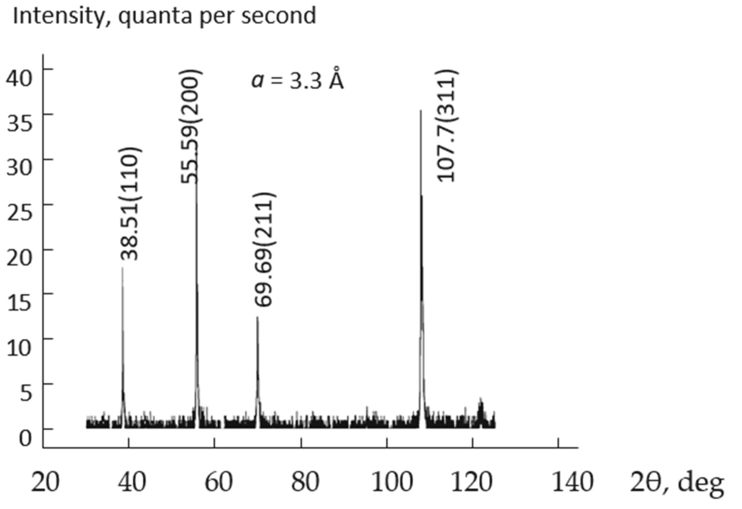
To clarify the nature of the double refraction of X-rays in polished tantalum radiograph of TER of X-rays (Figure 2) is compared with the corresponding X-ray diffraction pattern shown in Figure 3.
This X-ray diffraction pattern corresponds to polycrystalline cubic structure tantalum with a lattice constant a = 3.321( ± 0.0005 )   Å. For the quantitative interpretation of the anomalous double refraction effect on the radiograph of TER of X-rays for polished tantalum (Figure 2), the maximum intensities of four diffraction reflexes I h k l are theoretically considered. Taking into account the theoretical concepts of X-rays physics [20,22], the intensity of Bragg reflexes I h k l is proportional to the number of crystallites N c r h k l according to the ratio in the SI system:
N c r h k l = 1.59   × 10 18 I h k l sin   θ sin   2 θ f 2 p ( 1 + cos 2 θ )
where θ is the Bragg diffraction angle; f2 is the square of the atomic X-ray scattering factor from the crystallographic plane hkl; p is the repeatability factor of the crystallographic plane hkl.
Since, as has been repeatedly emphasized, the depth x of the formation TER of the X-rays is small and much less than the depth H h k l of X-ray diffraction, then, to interpret the effect of double refraction on TER of the X-ray for polished tantalum, one should take into account the number of surface crystallites N c r s h k l , which are x H h k l times smaller than the volume ones (7), and equal to:
N c r s h k l = x H h k l N c r h k l
For tantalum from the tables of Blokhin [21] and Katsnelson [23], the following data were determined: the mass absorption coefficient μ ρ = 162 cm 2 g ; density ρ = 16.6 g cm 3 .
Substituting the values of these parameters into the Equation (5), two output depths of the X-rays tested by the TER are calculated, corresponding to two maxima (1 and 2) of the TER of X-rays (Figure 2):
x 1 = 6.46   Å   x 2 = 50.9   Å
For the four observed reflexes on the tantalum X-ray diffrraction pattern (Figure 3) using the values of atomic X-ray scattering factors from the tables on Radiography edited by A. A. Katsnelson [24], the Table 1 shows all the values calculated by Equations (2), (5) and (6)–(8).
In the X-ray radiograph TER of X-rays for polished tantalum shown in Figure 2, the ratio of the intensities of the two maxima I 2 I 1 = 5.6 , which is close to the ratio of the number of surface crystallites with crystallographic planes (200) and (222) N c r s 200 N c r s 222 = 3.8 , given in the Table 1, which indicates that the double refraction shown in Figure 2 is due to the total external reflection of X-rays from two types crystallites with crystallographic planes (200) and (222). Therefore, taking into account the above relations and the data in Table 1, two different decrements of the refractive index of X-rays correspond to reflections from different crystallographic planes and correspond to the reflection at a large angle α 2 (large maximum) with a large decrement of the refractive index of X-rays δ 2 = 23   ×   10 8 and with a large interplane distance d 200 = 1.6511   Å occurs from the plane (200), and the reflection at a smaller angle α 1 (small maximum) with a small decrement of the refractive index δ 1 = 13.3   ×   10 8 and with a smaller interplane distance d 222 = 0.9535   Å occurs from the plane (222). Thus, for TER of X-rays from polished tantalum, there is a direct dependence of the decrement of the refractive index of X-rays on the interplanar distance. Studies of a number of metals [25], including nickel, copper, silver, platinum, bismuth, have shown that for all these materials just as for tantalum, the decrements of the refractive index of X-rays are directly proportional to the interplanar distances.The linear function in this case is represented by a simple relation δ = Cd, where C is the proportionality coefficient. Table 2 shows the values of the decrements δ of the refractive index of the X-rays of all the metals studied, the interplane distances d, constants C, absolute errors ∆C and the depth of output of X-rays x , experienced by TER.
According to Table 2, the average value of the coefficients C is calculated equal to C ¯ = 13 and, subtracting this average from the values of the coefficients for different metals, we obtain absolute errors for them ∆S. Averaging these errors, we get C ¯ = ± 1.3 .
Thus, it can be argued with good reason that a general law for solids is established for the direct proportional dependence of the decrement of the refractive index δ of X-rays on the interplane distance d in polycrystalline metals, which is expressed by the formula:
δ = C d ,   where   C = 13 ± 1.3

1.2. Ideas about the Excitation of Surface Plasmons in Solids by X-rays

The total external reflection of X-rays, which is a purely surface effect with output depth of less than 150 Å, is capable of exciting surface plasmons in solids. As indicated in the introduction, surface plasmons are actually excited by slow electrons, which are formed as a result of X-ray photoelectric effect enriched with bundles of slow secondary electrons.

1.2.1. Theoretical Concepts of Plasma Oscillations in Metals

The theory of plasmons in metals is based on a one-electron approximation based on the Drude-Lorentz theory of metals [26].
According to this theory, the static conductivity σ 0 at the frequency of the electromagnetic field ω = 0 is determined by the ratio:
σ 0 = N 0 e 2 τ m
where N 0 is the electron density in the volume of a solid; e and m are the charge and mass of the electron, respectively; τ is the relaxation time of the electron in the conduction band. The values of static conductivity in metals are determined in the Kei and Labi handbook [27] by resistivity ϱ = 1 σ 0   ~   10 8   Ω   ×   m for metals, and the bulk density of electrons conduction electrons N 0   ~   10 28   M 3 . Taking into account these data, the relaxation time τ is calculated using the Equation (9), which compose on the order 10 14   s .
According to the electronic theory of metals [26,28], high-frequency conductivity is a complex quantity and is expressed by the ratio:
σ ( ω ) = σ 0 1 i ω τ
where σ 0 is the static conductivity determined by the Equation (9). From Maxwell’s equations for high-frequency electromagnetic fields [26], the dielectric constant function ε(ω), as well as the high-frequency conductivity, is a complex quantity and, taking into account Equation (10), is determined by the ratio:
ε ( ω ) = 1 + 4 π i σ 0 ω ( 1 i ω τ )
In [29] X-ray radiation CuKα1 with a wavelength λ = 1.5406 Å was used, which corresponds to the angular frequency ω = 2πc/λ ~ 1019 s−1 and taking into account the above estimate of the magnitude τ , the product of ωτ in Equation (10) is of the order of 10 5 1 . Therefore, the unit in the denominator of Equation (11) can be neglected. Therefore, the function ε(ω) becomes real and, taking into account the Equation (9), is expressed by a simple relation [2,30]:
ε ( ω ) = 1 4 π σ 0 ω 2 τ = 1 ω P 2 ω 2 = 1 E P 2 E 2
where, according to the theory of plasmons [2,26], the square of the angular frequency of plasma oscillations of conduction electrons is determined by the expression ω P 2 = 4 π N 0 e 2 m ; E P = ω P [31] is the energy of the plasmon; E = ω = 8048   eV is the energy of incident X-ray radiation. From the ratio for ω P 2 it is possible to calculate the density of conduction electrons forming surface plasmons by the formula:
N = mE P 2 4 π 2 e 2 sin   α
Since in our work [29] surface plasmons in solids are excited by X-rays that have experienced TER, then in Equation (13) for the density of conduction electrons N, the right part must be multiplied by sin   α , where angle α is the angle of slip of the beam of X-rays that have experienced TER X-rays.
According to the electrodynamic theory of propagation of plane electromagnetic waves [2,30], the solution of Maxwell’s equations for a solid leads to a complex value of the wave number:
k = ω c ε + 4 π i σ 0 ω = ω n c
Hence the complex refractive index n is expressed by the ratio:
n = ε + 4 π i σ 0 ω
The estimation of the imaginary term in the root expression for n, expressed by the Equation (15), taking into account the above values of the resistivity of metals ϱ = 1 σ o and the angular frequency ω of the incident X-ray radiation gives:
4 π σ 0 ω   ~   10 10 1
It follows from this estimate that the imaginary term in then expression for n can be neglected and then the relationship between the refractive index and the permittivity will be expressed by a simple relation [28]:
n = ε
Taking into account this simplest relation, taking into account the Equation (12) for the value ε and the simple ratio (1) of geometric optics for the refractive index of X-rays, it is not difficult to determine the energy of plasma oscillations expressed as a function of the experimentally measured angle α:
E P = E 1 cos 2 α = E   ×   sin   α
Table 3 for metals shows the experimental angles α, the energy of plasmons E P , calculated by the Equation (17), the depth of their formation x , calculated by the Equation (5) and the density of conduction electrons N forming plasmons in certain crystallographic planes, calculated by the Equation (13).
From the analysis of the data given in Table 3, it follows that the observed dimensional effect is expressed in an increase in the energy of plasmons and the density of conduction electrons forming surface plasmons with an increase in the depth x of output of surface plasmons.

1.2.2. Plasma Oscillations in Crystalline Semiconductors and Dielectrics

Surface plasmons in crystalline semiconductors and dielectrics differ from polycrystalline metals by lower plasmon energies and much lower densities (by several orders of magnitude) of plasma electrons. This is due to the difference from metals in the spectrum of energy states of semiconductors and dielectrics, characterized by a band structure with a band gap of the largest width in dielectrics [2,32]. Obtained experimental and calculated data on plasma oscillations in single crystals of three semiconductors and in a single crystal of an alkaline halide compound of lithium fluoride are given in Table 4, where the values of the energy of plasmons E P , the depth x of excitation of plasmons and the density N 2 of valence electrons that make up plasmons are given.
The analysis of the data given in Table 4 shows that, by analogy with metals, a dimensional effect is observed for narrow-band crystalline semiconductors. In a single crystal of a LiF dielectric, the dimensional effect is most pronounced, which is due to the large band gap E g = 14.5   eV for lithium fluoride. It is noted in [33] that a significant difference between slow electrons exciting plasmons in dielectrics and metals is a significantly greater depth of the exit zone of such slow electrons in LiF, about 80 Å, which practically coincides with the depth X = 62.3 Å of excitation of plasmons in LiF according to our data [34].

2. Dispersion of Surface Plasmons in Solids

The study of surface plasmon dispersion opens up new possibilities for the studying the surface of solids of various types: metals, semiconductors and dielectrics by the method of plasma oscillations excited by X-rays that have experienced total external reflection. The dispersion of plasmons is the basis for understanding the role of electromagnetic waves in the excitation of plasmons in solids.
The dispersion of plasmons is understood as the dependence of the energy of plasmons E P on their wave vector   k . Such a function E p ( k ) is otherwise called the dispersion relation. In a number of works [35,36], the possibility of excitation of bulk and surface plasmons in dielectrics in the optical and radio frequency ranges of electromagnetic waves has been shown. The dispersion ratios of plasmons excited by light were calculated mainly theoretically on the basis of the Drude theory for free electrons in metals [37,38,39]. And only in two papers [40,41], the plasmon dispersion experimentally measured by inelastic X-ray scattering in a complex substance Nd 2 x Ce x CuO 4 appears to be a simple dispersion curve with a minimum at the wave vector k = 0 , and in the experimentally measured plasmon dispersion for glassy dielectrics such as fused quartz, quartz glass, uviol glass and molybdenum glass [34], in addition to simple dispersion curves, loop-like curves were also observed.
In our works [34,42], the dispersion of plasmons is represented by the dependence of their energy, measured at different azimuthal angles β, on the wave vector. In [39], where the dispersion of surface plasmons in structures with a conductive film was studied, the plasma wavenumber was introduced:
k P = ω P c = E P c
Here E p is the energy of plasmons in eV, measured by the method described in [29]; = 6.577   ·   10 16   eV   ×   s is Planck’s constant; c = 3   ×   10 8 m/s is the speed of light. Substituting the values of these constants into the ratio (18), taking into account the rotations of the sample in its plane along the azimuthal angle β in the range from 0° to 360° with a step of 22° and multiplying the wave number k P by cos β, we obtain the wave vector k P , defined by the formula:
k P = 5.06   ×   10 16   ×   E p     ×   cos   β   ( Å 1 )
The energy of plasmons in accordance with the variation of the sliding angle α with a change in the azimuth angle β was determined by the Equation (17). Unlike crystalline semiconductors and dielectrics with a band structure, in which the density of electronic states is different from zero only in the valence band and conduction band, and in the band gap is zero, amorphous solids are characterized by a different structure of electronic states, a characteristic feature of which are electronic states in the band gap, he so-called localized states. The concept of localized electronic states in amorphous bodies was theoretically developed in [43,44] and confirmed experimentally for amorphous fused quartz by spectroscopy in the ultra-soft region of the X-ray spectrum [45,46,47]. Visually localized states can be imagined as follows. In the physics of crystalline semiconductors and dielectrics it is known that defects in the crystal lattice lead to the appearance of discrete electronic states in the band gap [32]. In this regard, an amorphous dielectric can be represented as a crystal with a completely destroyed lattice and, consequently, with an infinite density of defective electronic states in the band gap, which form a continuous spectrum of localized states.
Thus, plasma oscillations in amorphous solids will be excited in localized electronic states.

2.1. Comparative Study of Plasmon Dispersion in Amorphous Fused Quartz and in a Single Crystal LiF

As an example, the dispersion of plasmons in amorphous fused quartz SiO 2 is considered. To analyze this dispersion relation, it is necessary to calculate some microscopic characteristics of SiO 2 . The mass absorption coefficient of X-rays in such a binary compound is calculated from the ratio [48]:
( μ ρ ) SiO 2 = M Si M ( μ ρ ) Si + 2 M O M ( μ ρ ) O
where the molar mass M of fused quartz is:
M = M Si + 2 M O = 60.06   g
Taking into account its components M Si = 28.086   g and M O = 15.99   g [23]. Taking into account the mass absorption coefficients of X-rays for elements forming silicon oxide [21] ( μ ρ ) si = 62.1   sm 2 g and ( μ ρ ) O = 11.3   sm 2 g , from the ratio (20) we obtain the mass absorption coefficient of X-rays for fused quartz:
( μ ρ ) SiO 2 = 35.054   sm 2 g
when the fused quartz density is ρ = 2.201   g sm 3 [49].Hence the linear absorption coefficient of X-rays in this case will be μ SiO 2 = 77.154   sm 1 , from the value of which the practical path of the X-ray quantum is determined in fused quartz is equal to R = 1 μ SiO 2 = 129.6   μ m . Knowing the value of the practical path of the X-ray quantum, a formula is obtained for calculating the depth of x TER of X-rays output and excitations of surface plasmons in fused quartz with plasmon excitation:
x = R 2 sin   α = 6.48   ×   10 3 sin α
It seems theoretically important to calculate the number of localized electrons involved in the formation TER of X-rays and in the excitation of plasma oscillations in a solid. The calculation is based on the well-known formula for the density of electrons localized in a solid body associated with the energy of plasmons [2,26]:
N 01 = mE P 2 4 π e 2 = 6.52   ×   10 26 E P 2
where E p is measured in electron volts. However, the electrons of a solid form TER of the X-ray and excite plasma oscillations only in a thin surface layer x with a volume V = s x , where s = 1.6   sm 2 is the area of illumination of the sample surface by a beam of incident X-rays in the TER mode. Then, taking into account the ratio (19), the number of localized electrons involved in the formation of TER of X-rays and in the excitation of plasmons will be determined for fused quartz by the following ratio:
N 1 = N 0 s x = 6.76   ×   10 24 E P 2 sin   α
The energy of plasmons is calculated by a simple Equation (17)
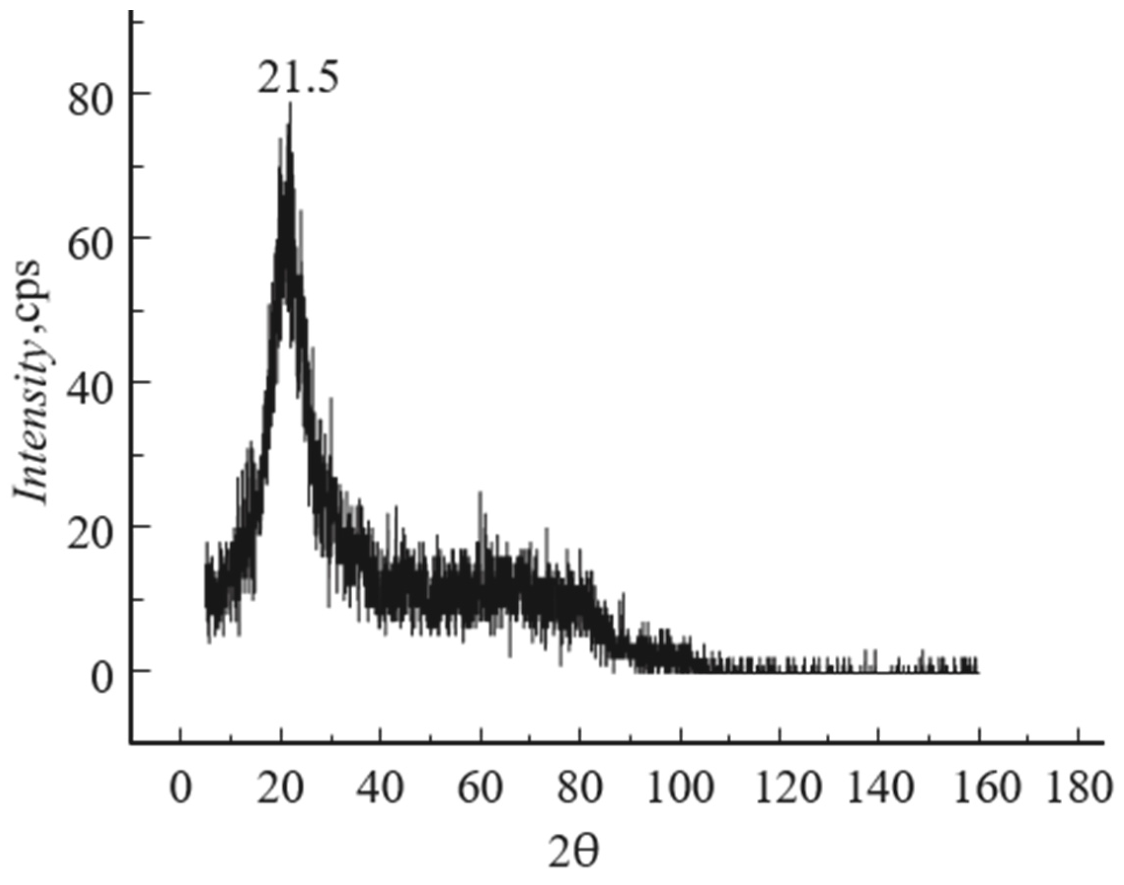
To prove the amorphousness of fused quartz, Figure 4 shows its X-ray diffraction pattern, which shows that fused quartz is indeed an amorphous solid with an observed halo at 2 θ = 21.5 ° . This corresponds to interference between pairs of silicon and oxygen atoms, the distance S between which calculated by the Curzom-Smith formula [50]:
S = 7.72 λ 4 π sin sin   θ g   Å
where λ = 1.5406   Å —the wavelength of the incident X-ray; θ g = 2 θ 2 = 10.75 ° —angular position interference halo.
The dictance between Si and O atoms calculated by Equation (24) is 5.07 Å.
Table 5 shows experimental and calculated data for fused quartz using Equations (17), (21) and (23).
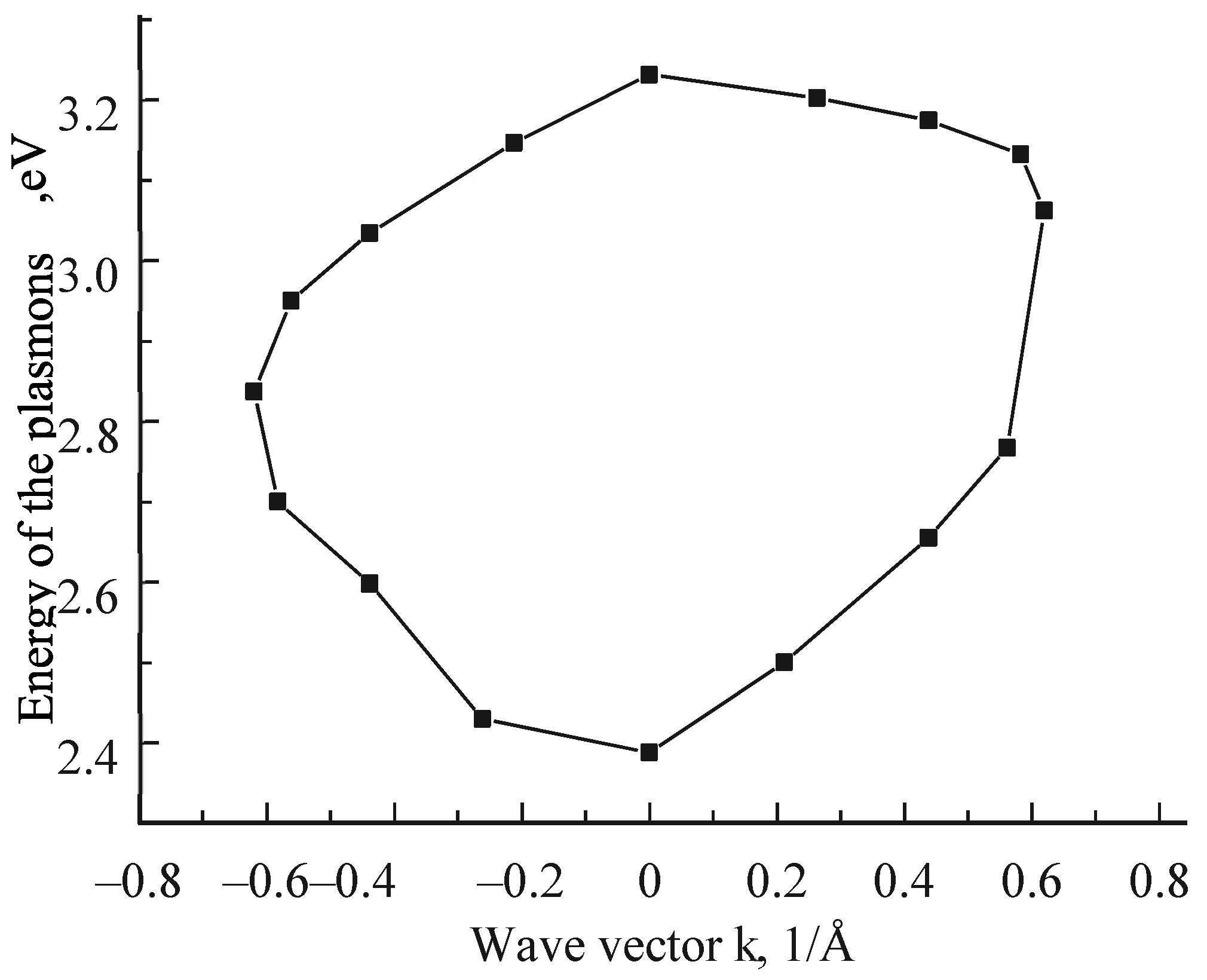
From Table 5 according to the experimental azimuthal angles β, the wave plasma vectors k P are calculated using the Equation (19) and dispersion curve of surface plasmons E P ( k P ) is constructed, shown in Figure 5.
The dispersion curve shown in Figure 5 has a loop-like appearance. Similar dispersion relations were observed on other glassy dielectrics [34].The average energy of plasmons is calculated from the area of this loop, using the empirical relation:
E P ¯ = i = 1 n E Pi n
where n = 30 is the number of steps along the axis of the wave vector.
The dispersion curve for fused quartz is characterized by a large area corresponding to the average energy of plasmons:
E ¯ P = 0.574   eV
In addition to this characteristic, from Table 5, where the ratios of the numbers of plasma electrons characterizing the asymmetries are given in four mutually perpendicular directions in the plane of the sample (along the angle β), it is possible to determine the value of the average electron asymmetry ( asym ¯ ) by averaging these ratios. This value characterizes the degree of spontaneous polarization of the test sample as a result its deformation. For fused quartz, according to Table 4, the average electron asymmetry was:
asym ¯ = 1.76
Such a large value of the average electron asymmetry in fused quartz is explained on the basis of the theory of polarizability of dielectrics [51], apparently by the deformation of amorphous fused quartz. According to this theory, there are two polarization mechanisms in dielectrics: atomic polarization, associated with the displacement of electrons relative to nuclei and most pronounced in alkali-halide crystals, and deformation polarization, associated with the displacement of ions under the action of mechanical microstresses. In connection with the results obtained from the dispersion of plasmons, the question arises about the nature of the loop-like dispersion curves of fused quartz and other glassy dielectrics. For this purpose, a study of the dispersion of surface plasmons in a single crystal of lithium fluoride has been undertaken. X-ray diffraction pattern of the LiF crystal, shown in Figure 6, indicates a perfect single crystal of cubic symmetry, cut out along the crystallographic plane (200), with a high intensity of about 40,000 quanta/s. and a small half-width of the diffraction peak of the order of 10′.
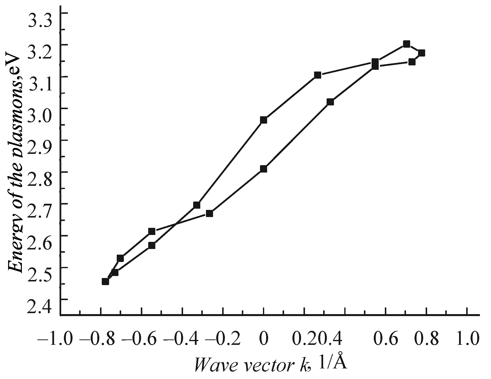
It turned out that the dispersion ratio for a single crystal LiF is very different from the dispersion of plasmons in fused quartz and is a very narrow loop that can practically be approximated by a straight line. Such a dispersion curve for a lithium fluoride single crystal is shown in Figure 7.
Processing of this narrow loop of plasmon dispersion for lithium fluoride using the empirical Equation (25) resulted in an abnormally low value of its average plasmon energy, which is almost two orders of magnitude less than the average energy of plasmons in fused quartz and is only:
E ¯ P = 0.0072   e V
However, the calculation of the average electron asymmetry in a lithium fluoride crystal taking into account the characteristics of lithium and fluorine atoms [21,23] according to a scheme similar to the calculation of fused quartz showed the value for LiF
asym ¯ = 1.74
which practically coincides with the corresponding characteristic of fused quartz. The large value of the average electron asymmetry of lithium fluoride is explained by the mechanism of dielectric polarization associated with the large dipole moment in the debs (D) of polar LiF molecules is equal to μ = 6.32   D , which is four orders of magnitude higher than the dipole moment of SiO2 molecules of fused quartz ( μ   ~   3   ×   10 4 ) [52]. Therefore, the great value of the asymmetry of fused quartz is apparently associated with the deformation mechanism of polarization.
To explain large difference in the average energies of plasmons between amorphous fused quartz and a single crystal of lithium fluoride, it is necessary to refer to the manufacturing technology of these solids. The paper [53] describes a method of purely chemical reactions for obtaining a single crystal of high-purity lithium fluoride of the brand “chda” with an alkaline halide compound LiF greater than 99%. Consequently, a single crystal of lithium fluoride with an almost zero value of the average plasmon energy should also have zero mechanical micro-stress. Unlike a single crystal of lithium fluoride, amorphous fused quartz and other glassy dielectrics are characterized by large average plasmon energies. This is apparently due to a different glass manufacturing technology. The paper [54] describes the technology of glass manufacturing by Fourcot and Float methods based on melting glass mass with its subsequent stretching. After cooling, the glass is distributed into pieces, which are then ground and polished. Such a technology of glasses obviously should lead to large internal micro-stress, which is expressed respectively in large values of the average energies of plasmons.
Thus, the average energy of plasma oscillations is proportional to the internal mechanical micro-stresses in the surface layers of solids. In this connection, the problem arises of quantitative relations between the average energy of plasmons and the value of internal micro-stresses. To solve this problem, we should consider the work [55], which shows the possibility of calculating using X-ray diffraction the values of micro-stresses σ parallel to the surface of the sample in a thin surface layer according to the formula:
σ = E Y ( a a 0 ) ( 1 γ ) a 0
where E Y is the Young’s modulus of elasticity; γ is the Poisson ratio; a is the experimental lattice constant; a 0 is the constant of the same lattice from the database.
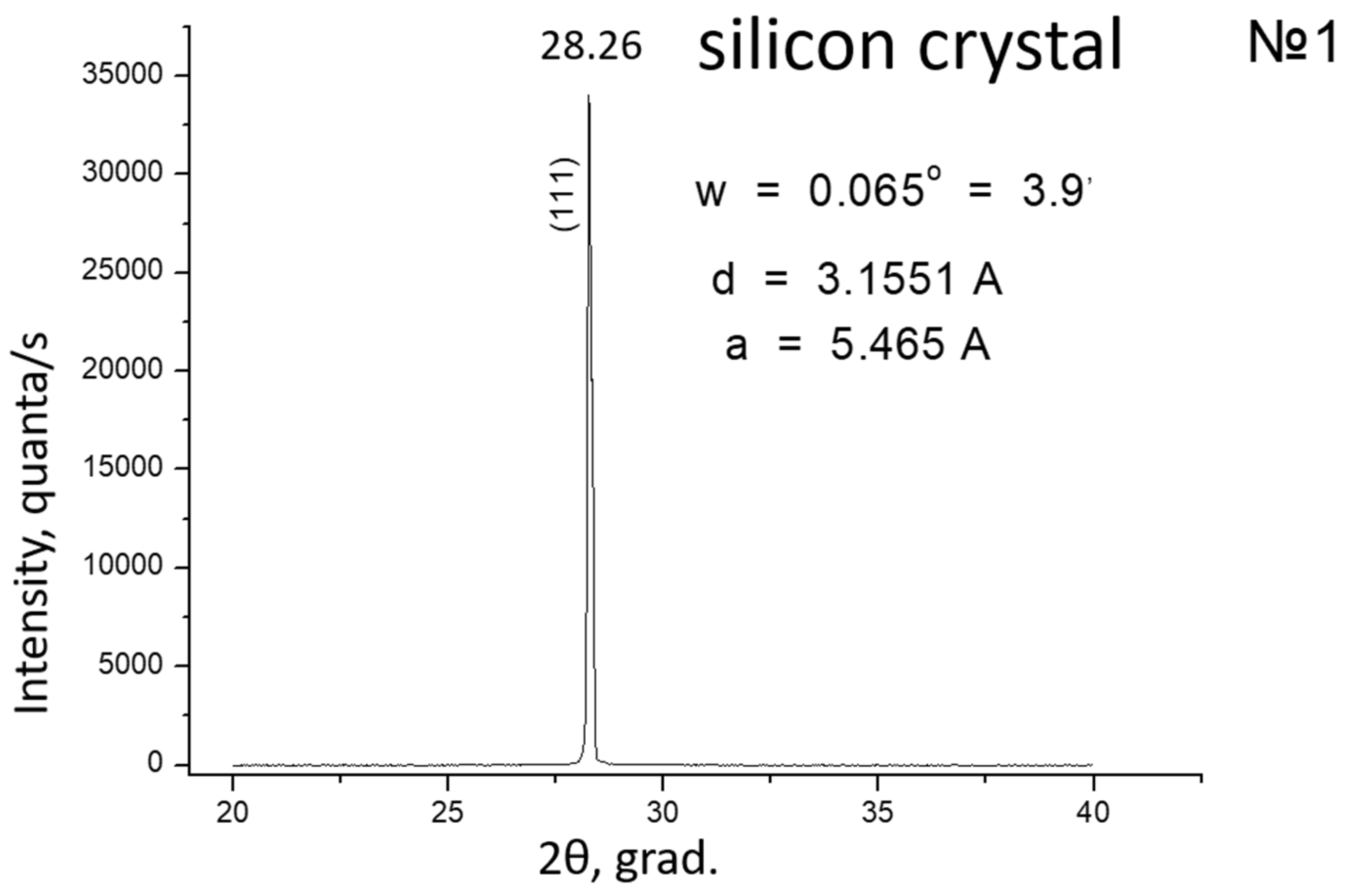
To solve the problem of the relationship between the average energy of plasmons and internal micro-stresses, it is necessary to choose a crystal standard. As such a standard, a single crystal of lithium fluoride is not suitable because of the almost zero average energy of plasmons. Therefore, a single silicon crystal was chosen as a reference, in which the average energy of plasmons is noticeably greater than zero. X-ray diffraction pattern of a single silicon crystal shown in Figure 8 indicates a perfect cubic crystal with a single diffraction reflex (111), whose intensity is 32,000 quanta/s and half-width is 3.9′.
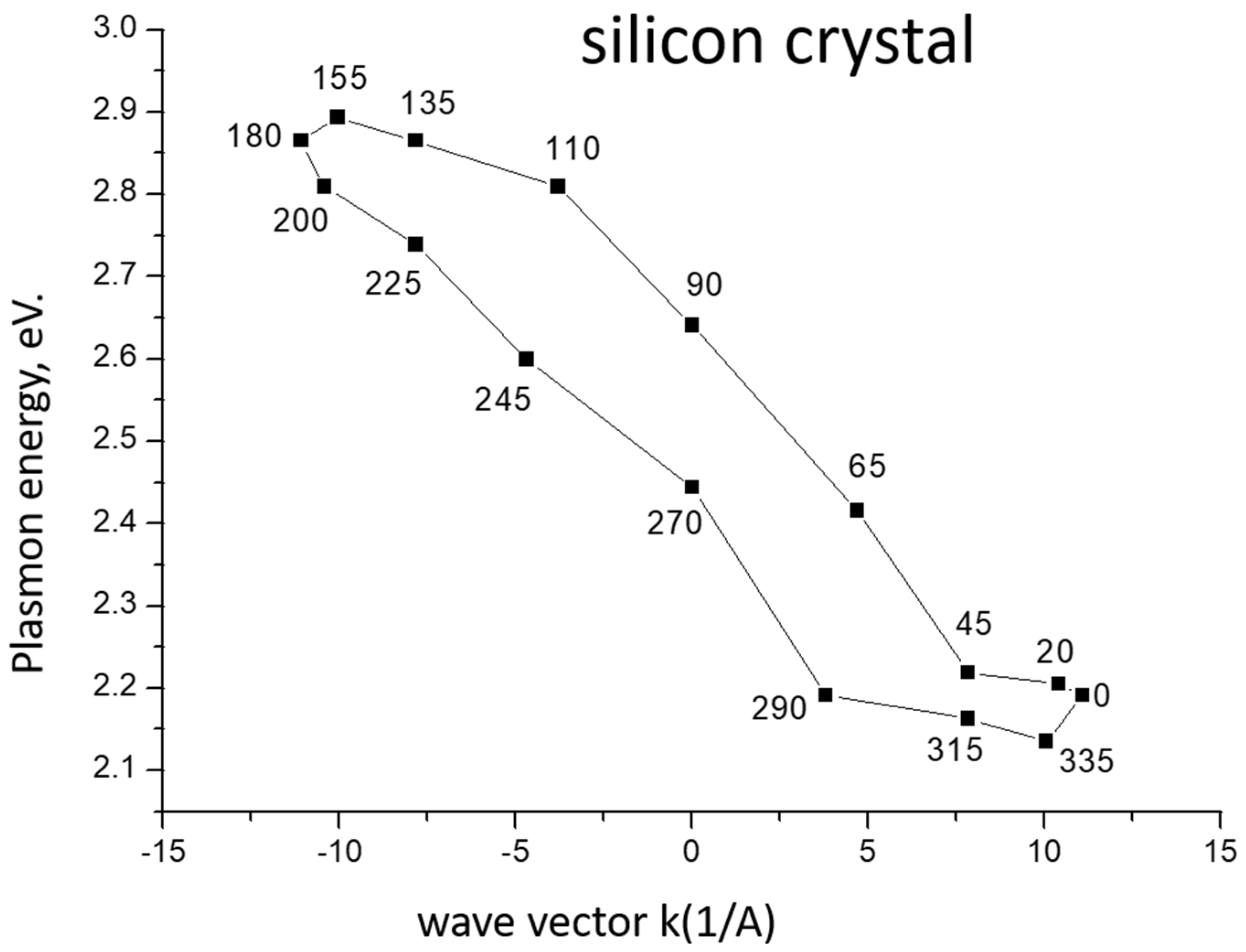
Calculated from the angular position of the diffraction peak 2 θ = 28.26 ° (Figure 8), the lattice constant of a silicon single crystal was a = 5.465   ( ± 0.0005 )   Å , and the lattice constant of the same crystal from the database is a 0 = 5.4301   Å . Taking into account the values a and a 0 , as well as the mechanical characteristics of the silicon crystal, including the Young’s modulus of elasticity E Y = 109   GPa ( GPa —gigapascal in Si system) and the Poisson ratio γ = 0.266 [56], the value of the micro-stress in a silicon single crystal equal to σ = 0.954   GPa is calculated by the Formula (26). This value of the micro-stress must be compared with the average plasmon energy, which for a single silicon crystal is calculated by the empirical Formula (25) from the plasmon dispersion curve shown in Figure 9.
The dispersion curve shown in Figure 9 is a closed loop-shaped curve, the area of which, calculated by the Equation (25), corresponds to the average energy of plasmons E ¯ P = 0.175   eV . Consequently, a single crystal of silicon as a reference is indeed a completely suitable object. Comparing the value of the average plasmon energy for a silicon single crystal with the calculated value for this crystal with a micro-stress σ = 0.954   GPa , the specific micro-stress in a silicon single crystal M σ is calculated using a simple ratio:
M σ = σ E P ¯ = 5.451   GPa eV
Thus, the ratio (27) completely solves the problem of coupling of the average energy of plasmons with the magnitude of the micro-stress. The value of the specific internal mechanical micro-stress (27) is taken as a reference and will be used for the calculation of micro-stresses in all future calculations.
Table 6 gives a summary of the average energies of plasmons and the corresponding values of micro-stresses calculated using the specific micro-stress M σ (Equation (27)) in all the studied glassy dielectrics, in a citall and in a single crystal of lithium fluoride,
In conclusion of the review, new experimental data on vanadium dioxides are considered.

2.2. Plasmon Dispersion in Amorphous Vanadium Dioxide VO2 Films

Two different samples of thin amorphous films with a thickness of about 10 nm of vanadium dioxide on a glassy sitall of two different modifications were studied using X-ray diffraction analysis and plasmon dispersion: one sample is a thin layer of vanadium dioxide №1 on a sitall substrate, and the second is a thin layer of vanadium dioxide №2 on a sitall with an aluminum sublayer.

2.2.1. Theoretical Calculations of Vanadium Dioxide

When studying the dispersion of plasmons, it is necessary to measure the energy of plasma oscillations excited by slow electrons with the most probable energy of 2–5 eV [14] using the TER of the X-ray method at sliding angles of incidence of the X-ray beam. In this case, the thickness of the surface layer where plasma oscillations occur can correspond to the exit zone of slow truly secondary electrons (TSE) X.
(1)
Calculation of the depth of the TSE X output.
The magnitude of the depth output from the solid body TSE X for simple monatomic substances is calculated by the formula Bronstein [33]:
X = 1.9   ×   10 7   ×   A ρ   ×   Z 0.6   ( Å )
where A is the atomic weight in grams; ρ is the material density in g/cm3; Z—number of the element. Since the ordinal number of the element Z is indeterminate for the binary compound VO2, the Equation (28) cannot be used for such a complex compound. Therefore, in this case, they are looking for a simple monatomic semiconductor with a band gap approximately equal to the band gap width of the binary compound under study. The band gap width of the narrow-band semiconductor VO2 is about E g = 0.5   eV close to the band gap width of the semiconductor tellurium Te with E g = 0.58   eV . Therefore, we will assume X V O 2 = X T e . The physical parameters of tellurium are as follows: A = 127.6 g; ρ = 6.24 g/cm3; Z = 52. Then the TSE yield zone for vanadium dioxide will be determined by the tellurium yield zone calculated by the Equation (28):
X V O 2 = X T e = 1.9   ×   10 7   ×   127.6 6.24   ×   10.7   ~   36   Å
(2)
Calculation of the depth x formation of TER X-rays.
The depth of the output X of the formation of TSE, calculated by the Equation (29), should be compared with the depth x of the formation of TER of X-rays. The calculation of the depth x is carried out in several stages. At the first stage, the mass absorption coefficient of X-rays for vanadium dioxide is calculated [48]:
( μ ρ ) VO 2 = M V M ( μ ρ ) V + 2 M O M ( μ ρ ) O
To calculate according to Equation (30), it is necessary to take into account all the values included in it [21,23,49]:
M = M V + 2 M O = 82.94   g
taking into account:
M V = 50.942   g M O = 15.999   g   ;
( μ ρ ) V = 228   sm 2 g   ;   ( μ ρ ) O = 11.3   sm 2 g   ρ VO 2 = 4.34   g sm 3
At the second stage, substituting the values given in the Equation (30), the value of the mass absorption coefficient of X-rays in vanadium dioxide is obtained equal to: ( μ ρ ) VO 2 = 144.354   sm 2 / g   .
Hence, taking into account the density of vanadium oxide, the linear absorption coefficient of X-rays will be:
μ VO 2 = 626.495   sm 1
At the third stage, the practical transverse path of X-ray quanta with an energy of 8048 eV in vanadium dioxide is calculated equal to:
R = 1 μ VO 2 = 15.961   μ m
And finally, at the fourth stage, the desired formula is obtained for calculating the depth of the output x of TER of theX-rays from vanadium dioxide in the form of:
x = R / 2   ×   sin   α x = 7.98   ×   10 4   ×   sin   α
(3)
Calculation of the number of electrons N involved in the excitation of plasmons in vanadium dioxide.
The number N is calculated by the general Equation (22):
N = N 01   ×   s   ×   x
where N 0 is the density of plasma localized electrons involved in TER of the X-ray; s = 1.6 sm2 is the area of illumination of the sample surface by a beam of X-rays; x is the depth of the output of X-rays into the solid body at a sliding angle of incidence experienced by TER. Since the calculations of the depth of the output of x TER of the X-rays for both samples of vanadium dioxide, the same value x = 27 Å was shown, then x < X and therefore x = 27 Å should be put. Taking into account this circumstance, the ratio for the number of localized electrons N 1 participating in the excitation of plasma oscillations in vanadium dioxide, according to Equation (22), will have the following form:
N 1 = 2.504   ×   10 20   ×   E P 2   ×   sin   α

2.2.2. X-ray Diffraction Analysis of Samples of Vanadium Dioxide thin Films

The diffraction of X-rays from two samples of vanadium dioxide №1 and №2 on monochromatic radiation CuKα1 with a wavelength λ = 1.5406 Å was studied on an X-ray diffractometer DRON-7 with a copper X-ray tube. Figure 10 shows X-ray diffraction pattern of a thin amorphous film of vanadium dioxide №1 on a citall substrate.
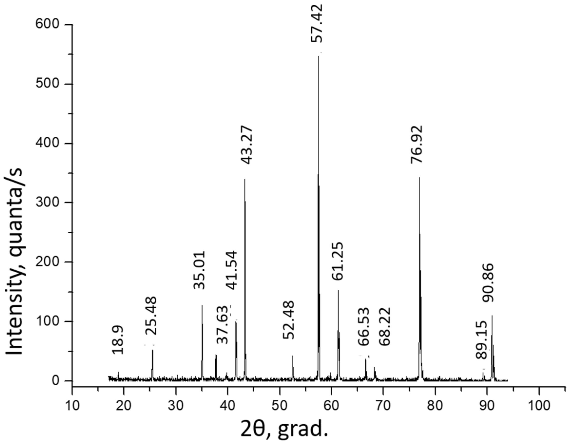
The X-ray diffraction pattern shown in Figure 10 shows the complete absence of an amorphous phase and corresponds to the diffraction from the substrate of a homogeneous glass crystal material of a citall with a polycrystalline phase of Al 2 O 3 .
Figure 11 shows a X-ray diffraction pattern for the second sample of a thin vanadium film №2 on a sitall with an aluminum sublayer.
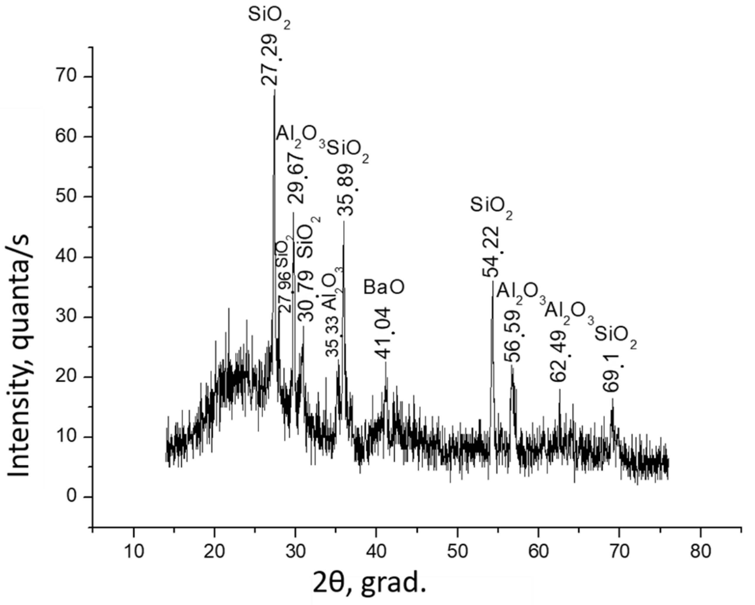
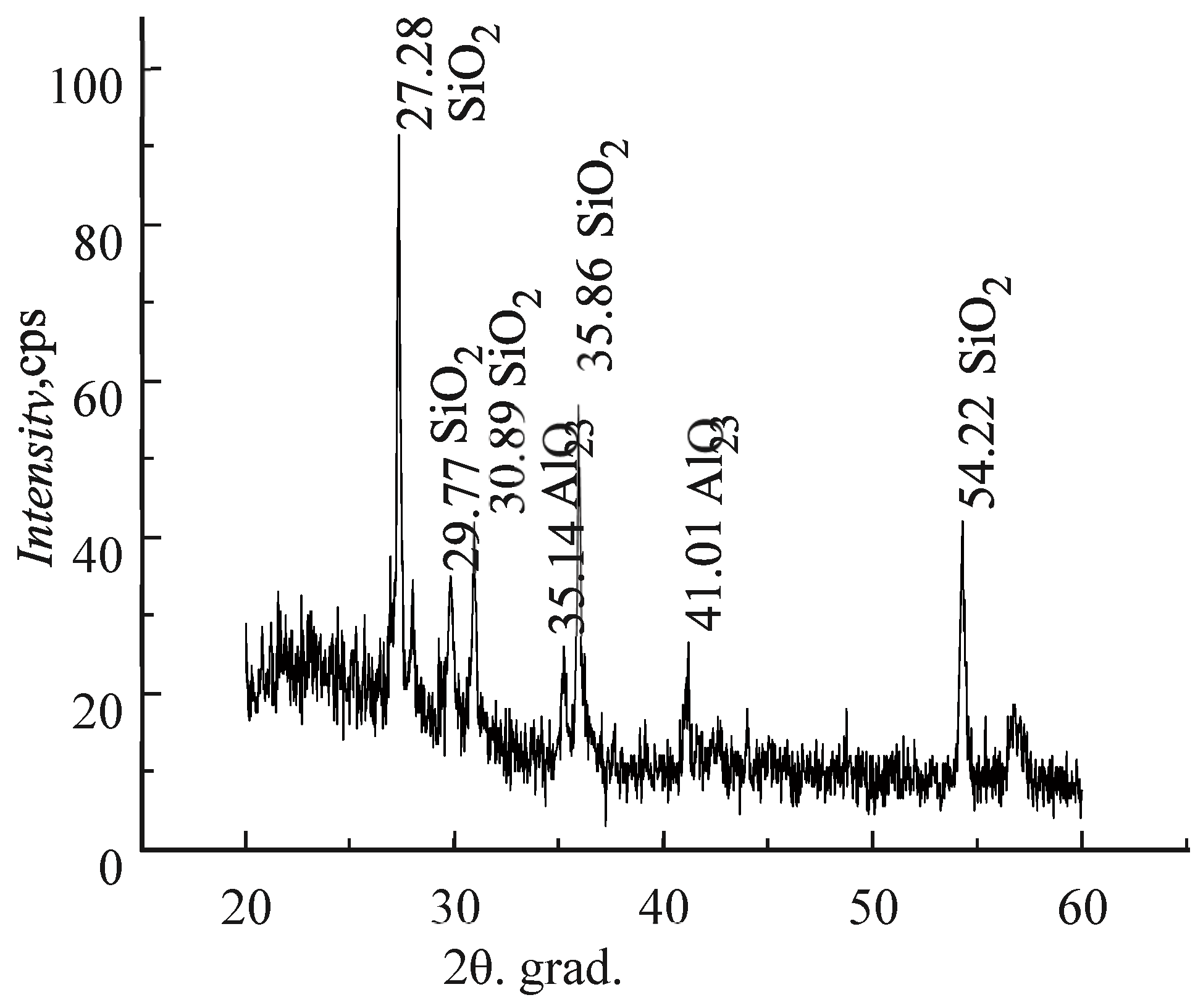
The X-ray diffraction pattern shown in Figure 11 for the thin film vanadium dioxide №2, in contrast to the sample of vanadium dioxide №1, shows a halo at 2θ 22°, characteristic of the amorphous phase of a glass crystal sitall, which contains similarly pure sitall, two crystalline phases: Al 2 O 3 and SiO 2 . For comparison with the X-ray diffraction pattern for the thin film №2 of vanadium dioxide (Figure 11), Figure 12 shows a X-ray diffraction pattern of pure citall, qualitatively similar to diffraction pattern shown in Figure 11 for the thin film №2 vanadium dioxide.
Since the X-ray diffraction analysis method, characterized by a diffraction depth of at least 1000 nm, exceeds the thickness of vanadium dioxide films by two orders of magnitude, it cannot determine by this method the structure of thin vanadium dioxide films with a thickness of about 10 nm. Therefore, it is possible to study such thin films only by the method of total external reflection of X-rays at a sliding angle of incidence of an X-ray beam with an analysis depth of about 3 nm.

2.2.3. Investigation of the Dispersion of Surface Plasmons by the Method of Total External Reflection of X-rays from Samples of Vanadium Dioxide Thin Films

At sliding angles of incidence of the order of 1′ of the primary X-ray radiation, the dispersion of surface plasmons for two samples of vanadium dioxide thin films was investigated by the method of total external reflection of X-rays.
Table 7 shows experimental and calculated data for a thin film of vanadium dioxide №1. Calculations were performed using Equations (17), (31) and (32).
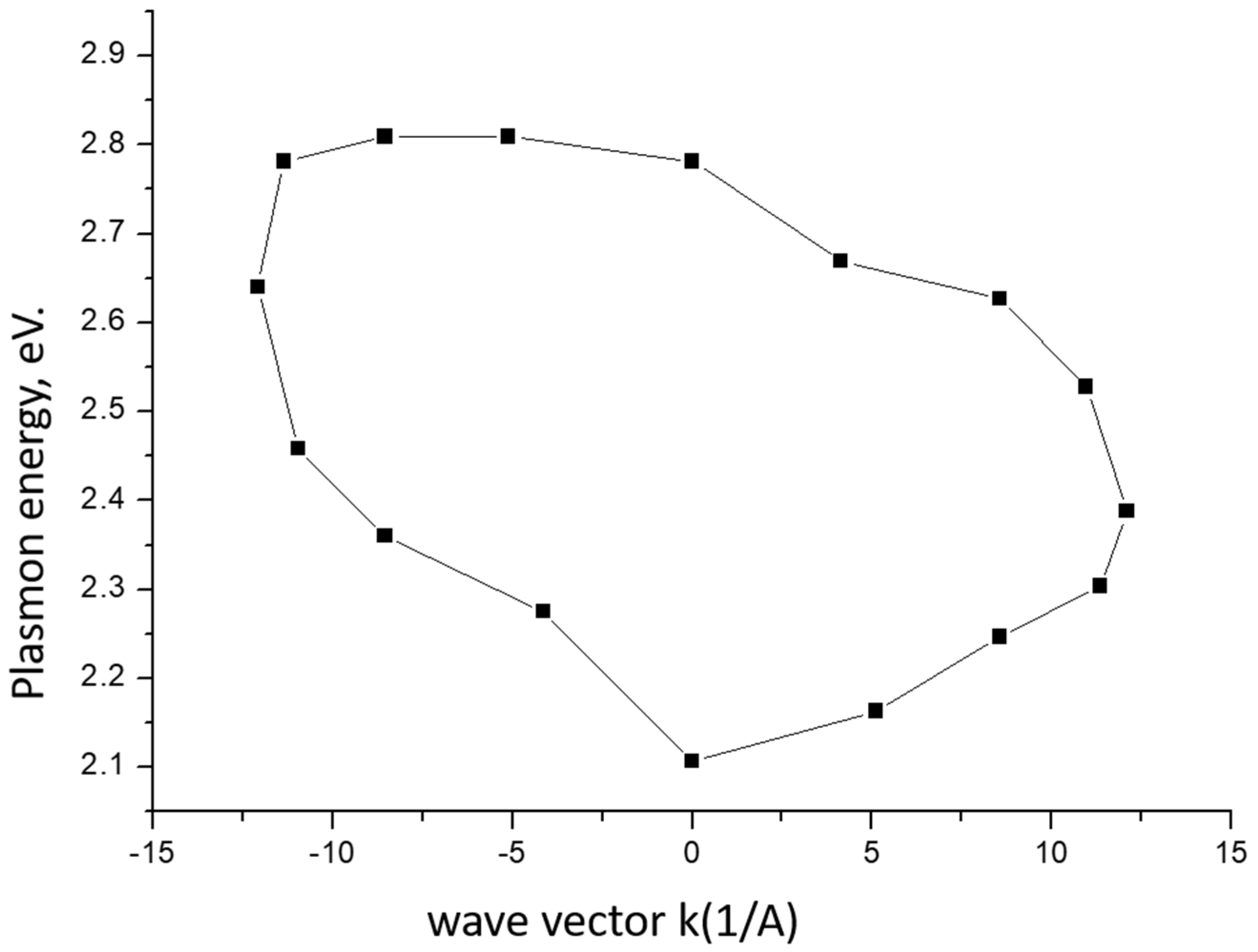
According to the averaged data of the 6th column of this table, the average electron asymmetry of a thin film of vanadium dioxide №1 turned out to be much greater than one and equal to asym ¯ = 1.745. According to Table 7, a plasmon dispersion curve is constructed, which is shown in Figure 13.
The dispersion of plasmons shown in Figure 13 for a 2.7 nm thick surface layer of a thin film of vanadium dioxide №1 on a glassy crystal is a loop-like curve with a large area S, within which the average energy of plasmons calculated by the empirical Formula (25) is E P ¯ = 0.517 eV. Calculated from this value of the average energy of plasmons by Equation (27) the magnitude of the micro-stresses in the surface layer of a thin film of vanadium dioxide№1 will be equal to σ = 3.86 GPa. Table 8 shows experimental and calculated data for a thin film of vanadium dioxide №2. The calculation of microscopic parameters was carried out according to the same formulas as for Table 7.
Calculated from the ratios of the number of plasma localized electrons shown in Table 8, the average electron the asymmetry for a thin film of vanadium dioxide №2 is asym ¯ = 1.98.
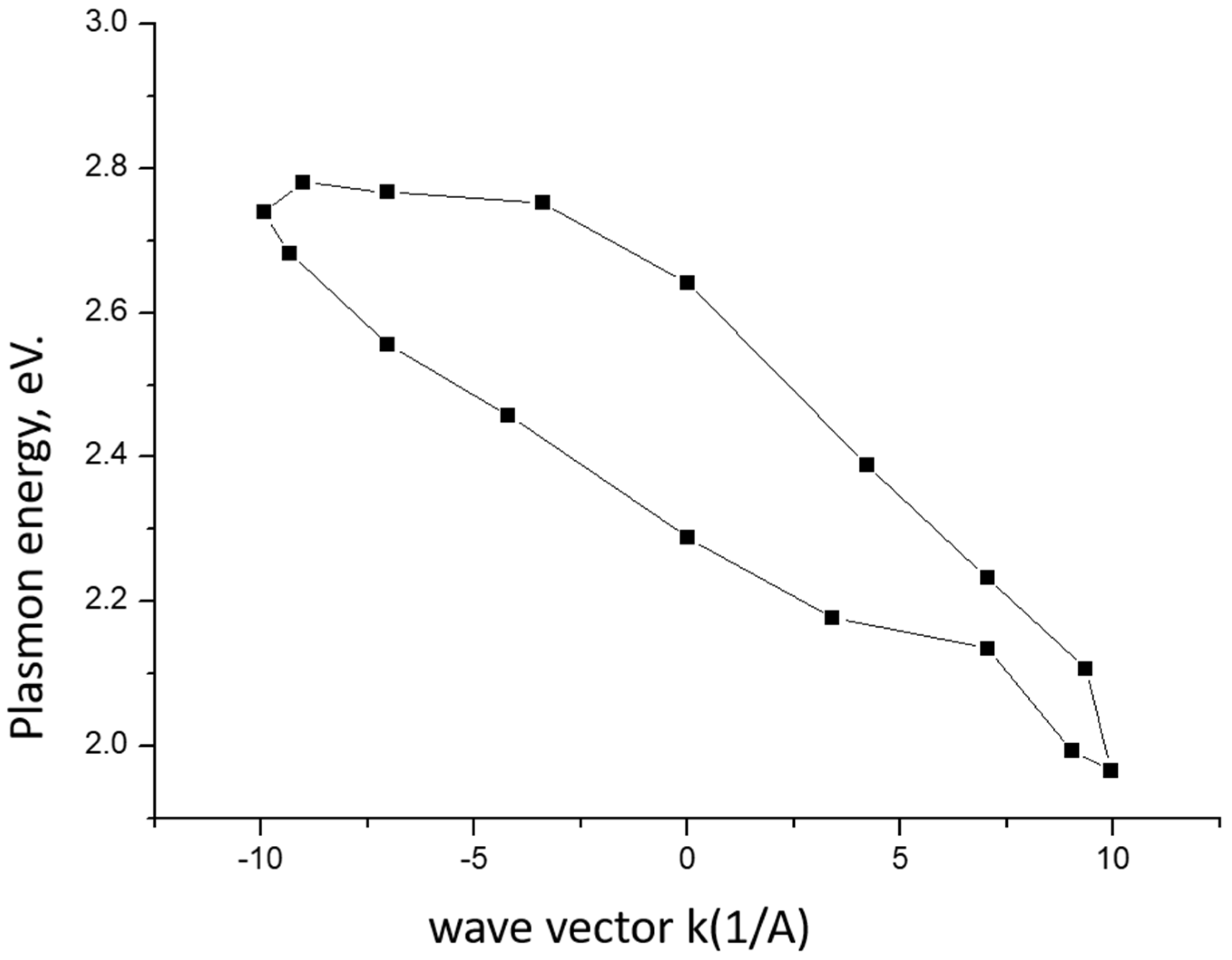
The dispersion of plasmons measured on the second sample of a thin film of vanadium dioxide №2 on a sitall with an aluminum sublayer has a slightly different appearance compared to the first sample. Figure 14 shows the dispersion curve for the second sample, calculated according to Table 8.
The plasmon dispersion shown in Figure 14 for vanadium dioxide №2 is a loop-like closed curve with a relatively small area, within which the average plasmon energy equal to E ¯ P = 0.23   eV is calculated by Equation (25).
From the obtained value of the average energy of plasmons, the value of the internal micro-stresses σ in a thin film of vanadium dioxide №2 is calculated by the Equation (27). For this material σ = 1.506 GPa.
At the conclusion of the X-ray studies of thin amorphous vanadium dioxide films, a comparative analysis of the results plasmon dispersion of two studied samples of vanadium dioxide thin films is carried out. Table 9 shows the results of a comparative analysis of these samples.
X-ray diffraction analysis of amorphous vanadium dioxide thin films showed that in both samples of vanadium dioxide thin films, observed only crystalline the structure of the substrate, since the depth of X-ray diffraction analysis is more than 2 orders of magnitude greater than the thickness of a thin film of vanadium dioxide. Moreover, as it turned out, the crystal structures of the substrates are different for different samples (Figure 11 and Figure 12). This means that different polytypes of sitals were used as substrates in both studied samples of thin film of vanadium dioxide. In the first sample with a thin film of vanadium dioxide №1, the substrate is a homogeneous citall with a polycrystalline phase of aluminum oxide Al 2 O 3 and with a complete absence of an amorphous phase. And in the second sample with a thin film of vanadium dioxide №2, a glass crystal sitall with two polycrystalline phases of aluminum oxide Al 2 O 3 and silicon oxide SiO 2 and with a large amorphous phase almost 80% similar to pure glass crystal sitall served as a substrate. The results of the study of pure glass sitll shown in the Figure 12.
The analysis of the results of studying the dispersion of surface plasmons and calculations given in Table 9 shows a decrease in the micro-stresess (and, accordingly, the average energy of plasmons) in the second sample by more than 2 times compared with the first. This proves the connection of micro-stresses in a thin film of vanadium dioxide with stresses in sitall substrates. The reduction of the micro-stresses in the second sample of a thin film of vanadium dioxide №2 is due to by shielding the stresses in the citall substrate with an aluminum sublayer. However, the electron mean asymmetry in both samples of vanadium dioxide thin films is almost the same and significantly greater than one, which indicates the same spontaneous polarizations in vanadium dioxide thin films due to the dipole moments of their molecules.

3. Conclusions

Classical electrodynamics describes with sufficient completeness the various aspekts of the phenomenon of diffraction of electromagnetic X-ray waves on crysnal structures. Thus, the intensity of diffraction reflexes calculated on the basis of the classical theory of elastic scattering of X-rays on electrons of crystalline bodies is sufficiently consistent with the experiment, and the angular position of the reflexes, using the inverse lattice concept, is determined with great accuracy by the Wolfe—Bragg equation: 2dsin θ = nλ, where d is the interplane distance in a bundle of crystallographic planes, from wich X-ray are reflected; θ is the Bragg diffraction angle; λ is the wavelength of X-rays; n is the diffraction order.
However, the excitation of surface plasma oscillations by X-rays are a purely q u a n t u m effect. Based on the principle of wave-particle dualism known from q u a n t u m mechanics, the excitation of surface plasmons is carried out by slow electrons, into which X-ray quanta are converted, exciting the X-ray photoelectric effect, accompanied by secondary electron amplification.
The study of the dispersion relations of surface plasmons excited by X-rays h a s significantly expanded the possibilities of studying the properties of the surface o f solids. First of all, it is possible to determine the values of mechanical micro--stresses in the surface layers of solids and thin films by the method of plasmon dispersion, which lead to the formation of defects in surface lattices. Measurement by this method of electronic asymmetry carries information about spontaneous polarization in the surface layers of solids.
Thus, from this point of view, the method of dispersion of surface plasmons is unique and very promising for analysis of properties of surface layers of massive solids and thin films. The only condition for applying the method of dispersion of surface plasmons is the presence in the diffractometer of a parabolic mirror forming a narrow paraxial beam of X-rays with a divergence of about 1′, which allows us to obtain differential curves of the total external reflection of X-rays, which significantly increases the accuracy of measuring the energy of surface plasmons (up to the third decimal place).

Funding

This work was carried out as part of a state assignment and was supported by the Ministry of Science and Higher Education of the Russian Federation, project no. 3.5005.2017/VU.

Data Availability Statement

Not available.

Conflicts of Interest

The author declares that he has no conflict of interest.

References

  1. Davydov, A.S. Solid State Theory; Nauka: Moscow, Russia, 1976; 405p. [Google Scholar]
  2. Ziman, J.M. Principles of the Theory of Solids; Cambridge University Press: Cambridge, UK, 1964; 405p. [Google Scholar]
  3. Pines, D. Elementary Excitations in Solids; CRC Press: New York, NY, USA, 1963. [Google Scholar]
  4. Bronstein, I.M.; Krainsky, I.L. Angular dependence of characteristic losses in magnesium and barium. Izv. USSR Acad. Sci. Phys. Ser. 1976, 40, 1956–1958. [Google Scholar]
  5. Komnik, Y.F. Physics of Metal Films; Atomizdat: Moscow, Russia, 1979; 263p. [Google Scholar]
  6. Petrov, Y.N. Physics of Small Particles; Science: Moscow, Russia, 1989; 358p. [Google Scholar]
  7. Klimov, V.V.; Fizmatgiz, M. Nanoplasmonics; Fizmatgiz: Moscow, Russia, 2009; 480p. [Google Scholar]
  8. Ramanavieius, H.; Herberg, F.W. Acta Med. Litnavica 2005, 12, 1–22. [CrossRef]
  9. Raether, H. Surface plasma oscillations and their application (A Review). Phys. Thin Film 1977, 12, 154. [Google Scholar]
  10. Kittel, C. Quantum Theory of Solids; John Wiley & Sons, Inc.: New York, NY, USA; London, UK, 1963; 485p. [Google Scholar]
  11. Gildenburg, V.B.; Kostin, V.A. Bulletin of the I.A. Lobachevsky Nizhny Novgorod Univ. 2011, 5, 314–322. [Google Scholar]
  12. Rumsh, M.A.; Shchemelev, V.N. The role of secondary emission processes in the X-ray photoelectric effect of metal cathodes. FTT 1963, 5, 71–75. [Google Scholar]
  13. Shchemelev, V.N.; Eliseenko, L.G.; Denisov, E.P.; Rumsh, M.A. On current and pulse measurements of X-ray photoemission of a massive cathode. FTT 1964, 6, 2574–2579. [Google Scholar]
  14. Stozharov, V.M.; Khinich, I.I. On the Mechanism of Excitation of Plasma Oscillations in Solids Investtigations with Total External Reflection of X-rays. Phys. Solid State 2021, 63, 794–796. [Google Scholar] [CrossRef]
  15. Compton, A.H. CXVII. The total reflexion of X-rays. Phil. Mag. 1923, 45, 1121. [Google Scholar] [CrossRef]
  16. Linnik, W.H.; Laschkarev, W. Determination of the Refractive Index of X-rays from the Phenomenon of Total Reflection. Z. Phys. 1926, 38, 659–671. [Google Scholar] [CrossRef]
  17. Raznomazov, V.M. Abstract of the Dissertation Microstructure and Elemental Analysis of Films Based on Oxides with the Structure of Perovskite According to X-ray Fluorescence Analysis with Full External Reflection; Southern Federal University: Rostov-Don, Russia, 2010; 52p. [Google Scholar]
  18. Stozharov, V.M. Total External Reflection of X-Rays from Solid Surfaces. Tech. Phys. 2017, 62, 152–156. [Google Scholar] [CrossRef]
  19. Parrat, L.G. Surface Studies by Total Reflection of X-Rays. Phys. Rev. 1954, 95, 359–369. [Google Scholar] [CrossRef]
  20. James, R.W. The Optical Principles of the Diffraction of X-rays; George Bell & Sons Ltd.: London, UK, 1950; 572p. [Google Scholar]
  21. Blokhin, M.A.; Schweitzer, I.E. X-ray Spectral Reference; Nauka: Moscow, Russia, 1982; pp. 94–99. [Google Scholar]
  22. Blokhin, M.A. Physics of X-rays; Publishing House of Technical and Theoretical Literature: Moscow, Russia, 1957; 511p. [Google Scholar]
  23. Katsnelson, A.A. Scattering of X-rays by Condensed Media; Moscow State University: Moscow, Russia, 1991; pp. 16–19. [Google Scholar]
  24. Katsnelson, A.A. Radiography. A Special Practice; Moscow State University: Moscow, Russia, 1986; pp. 24–33. [Google Scholar]
  25. Stozharov, V.M.; Pronin, V.P. On the mechanism of total external reflection of X-rays from the surface of polycrystalline solids. Tech. Phys. 2017, 62, 1899–1902. [Google Scholar] [CrossRef]
  26. Ashcroft, N.W.; Mermin, N.D. Solid State Physics; Saaunders College Publishing: New York, NY, USA; London, UK, 1976; Volume 1, 848p. [Google Scholar]
  27. Kay, D.; Labi, T. Handbook of an Experimental Physicist; IL: Moscow, Russia, 1969; 420p. [Google Scholar]
  28. Grosse, P. Free Electrons in Solids; Mir Publishers: Moscow, Russia, 1982; 260p. [Google Scholar]
  29. Stozharov, V.M. Determination of plasma oscillations in metals by the method of total external reflection of X-rays. Tech. Phys. 2019, 64, 977–979. [Google Scholar] [CrossRef]
  30. Landau, L.D.; Lifshits, E.M. Electrodynamics of Continuous Media; State Publishing House of Technical and Theoretical Literature: Moscow, Russia, 1957; 509p. [Google Scholar]
  31. Levich, V.G.; Vdovin, Y.A.; Myamlin, V.A. Course of Theoretical Physics; Fizmatgiz: Moscow, Russia, 1962; Volume 2, 247p. [Google Scholar]
  32. Ridley, B.K. Quantum Processes in Semiconductors; Oxford University Press: Oxford, UK, 1982; 300p. [Google Scholar]
  33. Bronstein, I.M.; Freiman, B.S. Secondary Electronic Emission; Nauka: Moscow, Russia, 1969; pp. 244–245. [Google Scholar]
  34. Stozharov, V.M. Investigation of Plasma Oscillations in Glasslike Dielectric by Means of Total External Reflection of X-Rays. Tech. Phys. 2020, 65, 1071–1075. [Google Scholar] [CrossRef]
  35. Volkov, V.A. Plasmons and magnetoplasmons. In Influence on the Response of Semiconductor Structures in the Giga- and Terahertz Ranges; Kotelnikov Institute of Radioengineering and Electronics (IRE): Moscow, Russia, 2019; pp. 1–7. [Google Scholar]
  36. Lisitsa, V.S. Introduction to Nanooptics; Moscow Institute of Physics and Technology (MIPT): Moscow, Russia, 2012; pp. 104–112. [Google Scholar]
  37. Karalis, A.; Lidorikis, E.; Ibanesky, M.; Joannopoulos, J. Surface-Plasmon-Assisted Guiding of Broadband Slow and Subwafelength Light in Air. Phys. Rev. Lett. 2005, 95, 063901. [Google Scholar] [CrossRef] [PubMed] [Green Version]
  38. Eremin, M.V.; Kochergin, D.S. On the theory of plasmon dispersion in electronically dispersed cuprates. Lett. JETF 2018, 108, 119–123. [Google Scholar] [CrossRef]
  39. Davidovich, M.V. Dispersion of surface plasmons in structures with a conductive film. Opt. Spectrosc. 2019, 126, 360–369. [Google Scholar] [CrossRef]
  40. Baltar, H.; Drozdowicz, K.; Goldys, E.M. Propagating Surface Plasmons and Dispersion Relations for Nanoscale Multilayer Metall-Dielectric. In Plasmonics—Principles and Applications; Intechopen: London, UK, 2012; pp. 135–155. [Google Scholar]
  41. Lee, W.S.; Lee, J.J.; Nowadnick, E.A. Asymmetry of collective Excitations in electron and hole-doped cuprate. Nat. Phys. 2014, 10, 883–895. [Google Scholar] [CrossRef] [Green Version]
  42. Stozharov, V.M. Dispersion of Plasma Oscillations in Amorphous Chalcogenide Semiconductors. Tech. Phys. 2021, 66, 1035–1038. [Google Scholar] [CrossRef]
  43. Felts, A. Amorphous Glassy Solids; Mir Publishers: Moscow, Russia, 1882; 545p. [Google Scholar]
  44. Mott, N.; Devis, E. Electronic Processes in Non-Crystalline Materials; Oxford University Press: Oxford, UK, 1980; 350p. [Google Scholar] [CrossRef]
  45. Brytov, I.A.; Romashchenko, Y.N. X-ray spectral study of the electronic structure of silicon and aluminum oxides. Solid State Phys. 1978, 29, 664–672. [Google Scholar]
  46. Britov, I.A.; Gritsenko, V.A.; Romaschenko, Y.N. Short-range Order and Electronic structure of Amorphous SiNxOy. J. Exp. Theor. Phys. 1985, 62, 321–327. [Google Scholar]
  47. SNekrashevich, S.; Gritzenko, V.A. Electronic structure of Silicon dioxide (A REVIEW). Phys. Solid State 2014, 56, 207–222. [Google Scholar] [CrossRef]
  48. Klug, H.P.; Alexander, L.E. X-ray Diffraction Procedures; John Wiley and Sons, Inc.: New York, NY, USA; London, UK, 1954; 686p. [Google Scholar]
  49. Rabinovich, V.A.; Havin, Z.Y. A Brief Chemical Reference; Chemistry: Leningrad, Russia, 1970; 115p. [Google Scholar]
  50. Korsunsky, M.I. Physics of X-rays; ONTI: Moscow-Leningrad, Russia, 1936; 138p. [Google Scholar]
  51. Ashcroft, N.W.; Mermin, N.D. Solid State Physics; John Wiley and Sons, Inc.: New York, NY, USA; London, UK, 1976; Volume 2, pp. 166–170. [Google Scholar]
  52. The Soviet Encyclopedia; Knuniants, I.L. (Ed.) Sovetskaya Entsiklopediya: Moscow, Russia, 1990; Volume 2, 671p. [Google Scholar]
  53. Ostroushko, Y.N. Lithium, Chemistry and Technology; Chemistry: Leningrad, Russia, 1960; 234p. [Google Scholar]
  54. Schultz, M.M.; Mazurin, O.V. Modern Understanding of the Structure of Glasses and Their Properties; Science: Leningrad, Russia, 1988; 488p. [Google Scholar]
  55. Eckertova, L. Physics of Thin Films; Springer: Boston, MA, USA, 1984; 340p. [Google Scholar]
  56. Anuryev, V.I. Handbook of a Mechanical Engineer Designer; Mechanical Engineering: Moscow, Russia, 2001. [Google Scholar]
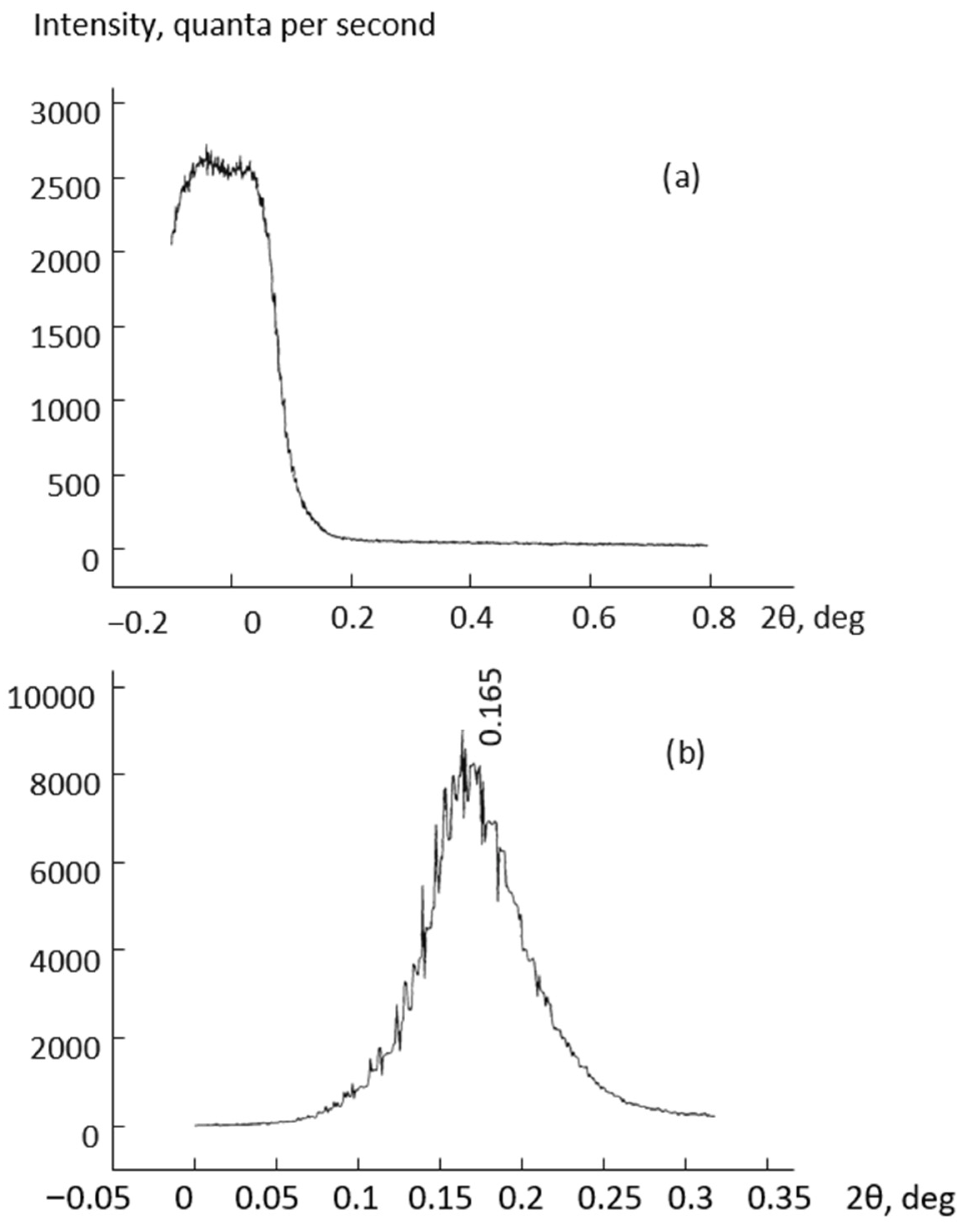
Figure 1. Silicon single crystal (111) with a face-centered lattice: (a) integral curve of TER; (b) differential curve of TER with an indication of an angle of 2 θ degrees above the maximum [18].
Solids 03 00009 g001
Figure 2. Radiograph of polished polycrystalline tantalum under conditions of total external reflection of X-rays with indication of sliding angles α in degrees above each maximum [18].
Solids 03 00009 g002
Figure 3. X-ray diffraction pattern for polished polycrystalline tantalum with indication of X-ray scattering angles 2θ-grad and Miller indices (hkl) of crystallographic planes above each diffraction peak [18].
Solids 03 00009 g003
Figure 4. X-ray diffraction pattern for fused quartz with an indication of the angle 2 θ = 21.5 ° of halos [34].
Solids 03 00009 g004
Figure 5. Dispersion of surface plasmons for fused quartz [34].
Solids 03 00009 g005
Figure 6. X-ray diffraction pattern of a lithium fluoride single crystal with indication of the X-ray scattering angle 2 θ = 44.89 ° and Miller indices (200) above the diffraction peak [34].
Solids 03 00009 g006
Figure 7. Dispersion of surface plasmons for a single crystal LiF [34].
Solids 03 00009 g007
Figure 8. X-ray diffraction pattern of a silicon single crystal with an indication of the X-ray scattering angle 2θ above the diffraction peak and the Miller index of the crystallographic plane.
Solids 03 00009 g008
Figure 9. Dispersion of surface plasmons for a silicon single crystal with indication of azimuthal angles β in degrees for each experimental point.
Solids 03 00009 g009
Figure 10. X-ray diffraction pattern of a thin amorphous film of vanadium dioxide №1 on a sitall with an indication of the X-ray scattering angles 2θ in degrees above each diffraction peak.
Solids 03 00009 g010
Figure 11. X-ray diffraction pattern of a thin film of vanadium dioxide №2 indicating the angles 2θ in degrees and the substance above each diffraction peak.
Solids 03 00009 g011
Figure 12. X-ray diffraction pattern of a pure glass crystal with an indication of the X-ray scattering angles 2θ in degrees and substances above each diffraction peak [34].
Solids 03 00009 g012
Figure 13. Dispersion of plasmons in a thin film of vanadium dioxide №1 on a sitall.
Solids 03 00009 g013
Figure 14. Plasmon dispersion for a thin film of vanadium dioxide №2 on a sitall with an aluminum sublayer.
Solids 03 00009 g014
Table 1. Experimental data on X-ray diffraction and results of quantitative calculations for polished tantalum [18].
Reflex Number2θ° h k l H h k l   ×   10 4 c m ( x H h k l )   ×   10 4 N c r s   ×   10 9 d ,   Å δ × 10−8
138.52741101.22735.26365.90572.3348
255.61902001.735529.3293842.31.651123.1
369.67652112.12513.039846.2191.3484
410.7712223.00522.1496971.910.953513.3
Here: 2θ—X-ray scattering angle; H h k l the depth of X-ray diffraction; x the depth of formation TER of X-ray; Ncrs—the number of surface crystallites; d interplane distance; δ decrement of the refractive index of X-rays.
Table 2. Calculated values of δ, d, C, ∆C and x.
Metal
δ   ×   10 8
d, Å
C = δ d   ×   10 8   Å 1
C   ×   10 8   Å 1
x ,   Å
Ni21.11.7542121143.4
Cu12.81.278610352.5
Ag26.32.023413072.18
Pt33.82.253715−217.90
Bi54.23.948214−110.99
δ decrement of the refractive index of X-rays; d interplanar distances; C constants; C absolute errors; x the depth of output of X-rays, experienced by TER.
Table 3. Experimental data on X-ray diffraction and calculation results for metals [29].
Metal α °   h k l   E P ,   e V x ,   Å N   ×   10 28   m 3
Cu0.01781112.06264.062
0.02612004.06528.707
Mo0.077620010.9427.723
Ta0.00952001.46.51.274
0.078522211.0507.865
Pt0.01411111.985.352.548
0.087822212.3335.09.909
Ag0.01241111.744.51.168
Au0.06122228.6020.14.807
α the angle of sliding of X-rays beam; E P energy of surface plasmons; x the depth of the output X-rays forming surface plasmon; N the density of conduction electros forming surface plasmons.
Table 4. Results of quantitative calculations of the characteristics of surface plasmons for crystalline crystalline semiconductors and dielectrics.
Semiconductor Crystals E P ,   e V x ,   Å N 2 E g ,   e V
Si2.14690.5 60.56   ×   10 16 1.120
Ge2.13532 40.87   ×   10 16 0.665
GaSb1.89612 13.25   ×   10 16 0.810
Dielectric Crystal
LiF3.17462.3 20.15   ×   10 21 14.50
E g the width of the forbidden zone; E P energy of surface plasmons; x the depth of the output X-rays forming surface plasmons; N 2 the density of valence electrons forming surface plasmons in crystalline semiconductors and dielectrics.
Table 5. Experimental data and results of quantitative calculations of characteristic of surface plasmons for fused quartz [34].
β ° α ° E P ,   eV x ,   Å N 1   ×   10 21   Electrons Electron Asymmetry
0 0.0218 3.062 246 24 N1(0) /N1(180) = 1.26

N1(45) /N1(225) = 1.8

N1(90) /N1(270) = 2.54

N1(135) /N1(335) = 1.44
20 0.0223 3.132 252 26
45 0.0226 3.174 256 27
65 0.0228 3.202 258 28
90 0.0230 3.231 260 28
110 0.0224 3.146 253 26
135 0.0126 3.034 244 23
155 0.0210 2.950 238 22
180 0.0202 2.837 228 19
200 0.0192 2.700 217 16
225 0.0185 2.598 209 15
245 0.0173 2.430 196 12
270 0.0170 2.388 192 11
290 0.0178 2.500 201 13
315 0.0189 2.655 214 16
335 0.0197 2.767 223 18
β experimental azimuth angle; α experimental angle of sliding incidence of X-rays; E P energy of surface plasmons; x the depth of TER of X-rays output with surface plasmons excitation; N the number localized electrons involved in the formation of TER of X-rays and in excitation of surface plasmons; in electronic asymmetries, azimuthal angles β in brackets are indicated.
Table 6. The results of calculations of the average energies of plasmons and microstresses in glassy dielectrics, single crystal LiF and sitall.
Substance E ¯ P ,   e V σ ,   G P a
fused quartz0.5743.129
quartz glass0.3952.153
uviol glass0.4122.246
molybdenum glass0.4322.354
lithium fluoride0.00420
sitall0.3611.968
E ¯ P average energy of surface plasmons; σ the values of micro-stresses parallel to surface of the in thin surface layers.
Table 7. Experimental data, plasmon energies and other microscopic characteristics of a thin film of vanadium dioxide №1.
β ° α ° E P ,   e V x ,   Å N 1   ×   10 16
Electrons
N1(0)/N1(180) = 1.35

N1(45)/N(225) = 1.95

N1(90)/N1(270) = 2.3

N1(135)/N1(335) = 1.38
00.01702.38823.6842.36
200.01642.30422.8438.04
450.01602.24722.2835.30
650.01542.16321.4531.76
900.01502.10720.8929.10
1100.01622.27522.5636.64
1350.01682.36023.4040.89
1550.01752.45824.3746.20
1800.01882.64026.1857.26
2000.01982.78127.5866.92
2250.02002.80927.8568.96
2450.02002.80927.8568.96
2700.01982.78127.5866.92
2900.01902.66926.4659.15
3150.01872.62726.0456.40
3350.01802.52825.0750.20
β azimuth angle; α experimental angle of sliding incidence of X-rays;   E P energy of surface plasmon; x the depth of TER of X-rays output with surface; p—plasmons excitation; N 1 the number localized electrons involved in formation of T E R of X-rays and excitation of surface plasmons; in electronic asymmetries, a z i m u t a l angles β in brackets are indicated.
Table 8. Experimental and calculated data for vanadium dioxide №2.
β ° α ° E P ,   e V x ,   Å N 1   ×   10 16
Electrons
N1(0)/N1(180) = 2.7

N1(45)/N1(225) = 1.5

N1(90)/N1(270) = 1.53

N1(135)/N1(335) = 2.18
00.01401.96619.5019.21
200.01502.10720.8922.64
450.01592.23322,1428.14
650.01702.38823.6834.42
900.01882.64126.1846.55
1100.01962.75327.3052.73
1350.01972.76727.4853.54
1550.01982.78127.5854.36
1800.01952.73927.1651.96
2000.01912.68326.6048.81
2250.01822.55625.3542.21
2450.01752.45824.3737.53
2700.01632.28922.7030.32
2900.01552.17721.5926.08
3150.01522.13521.1724.60
3350.01421.99419.7820.04
  β azimuth angle; α experimental angle of sliding incidence of X-rays; E P energy of surface plasmon; x the depth of TER of X-rays output with surface p plasmons excitation; N 1 the number localized electrons involved in formation of T E R of X-rays and excitation of surface plasmons; in electronic asymmetries, a z i m u t a l angles β in brackets are indicated.
Table 9. Comparison of the results of studying the dispersion of surface plasmons and calculating the microscopic characteristics for two samples of vanadium dioxide thin films.
Vanadium Dioxide Films a s y m ¯ E ¯ P ,   e V σ ,   G P a x ,   Å
№11.7450.5173.38627
№21.9800.2301.50627
Publisher’s Note: MDPI stays neutral with regard to jurisdictional claims in published maps and institutional affiliations.