Article

A Novel Combined Control Strategy for a Two-Stage Parallel Full-Wave ZCS Quasi Resonant Boost Converter for PV-Based Battery Charging Systems with Maximum Power Point Tracking

1
Department of Electrical and Computer Engineering, San Diego State University, San Diego, CA 92182, USA
2
Department of Electrical and Biomedical Engineering, University of Nevada Reno, Reno, NV 89557, USA
*
Author to whom correspondence should be addressed.
Electricity 2022, 3(1), 145-161; https://doi.org/10.3390/electricity3010009
Submission received: 5 November 2021 / Revised: 15 February 2022 / Accepted: 28 February 2022 / Published: 8 March 2022
(This article belongs to the Special Issue Recent Advances in Grid Connected Photovoltaic Systems)

Abstract

:
This work deals with the design and validation of a combined control strategy to satisfy the requirements for both soft switching and Maximum Power Point Tracking (MPPT) for a Photo Voltaic based (PV-based) battery charging system. The proposed controller is employed for a two-stage parallel full-wave Zero Current Switching (ZCS) quasi resonant boost converter to obtain maximum voltage using Perturb and Observation (P&O) method. The controller utilizes frequency modulation to regulate the output voltage, considering any changes experienced due to the intermittent nature of the PV system. Operating principles of the tow-stage parallel boost converter are thoroughly analyzed, and Matlab Simscape toolbox and its real-time workshop capability is utilized to evaluate the performance of the proposed controller for a battery charging system.

1. Introduction

In the past decade, renewable energy has witnessed a tremendous demand as a next generation energy source capable of reducing the impacts of energy exhaustion and global warming. Out of numerous renewable energy resources, solar energy is the most prevalent energy source widely adopted. Photovoltaic (PV) systems have been a prominent area of research to improve energy utilization and support the future demand of PV systems. Typically, a PV system is composed of a DC–DC converter, a maximum power point tracker (MPPT), and a battery for energy storage [1].
Nowadays, switching mode power supplies are incorporated in most renewable energy interfaces that are used in many applications throughout residential and industrial sectors [2,3,4,5]. It is of utter importance to accommodate to the increasing demand for small size, low cost and efficient switching mode power supplies. The switching transitions of conventional Pulse Width Modulation (PWM) converters are always lossy due to voltage and current stresses experienced during switching. Conventional boost converters operate using hard-switching to step up the voltage. The switching characteristics of the passive diode cause large spikes during turn-off and turn-on intervals by forcing the switch to have simultaneous nonzero voltage and current [6,7,8]. In addition to that, during hard-switching the MOSFET drain-to-source charge builds up during turn on, which further contributes to the switching losses.
Unlike hard-switching, power losses experienced by DC–DC boost converter can be eliminated using soft-switching techniques by operating the switch either at zero current or at zero voltage. By implementing Zero-Voltage Switching (ZVS) or Zero-Current Switching (ZCS) on DC–DC converters, numerous soft-switching techniques have been proposed to attain high efficiency by reducing switching losses [9,10,11,12]. By eliminating the overlap of current and voltage experienced by hard-switching, soft-switching is considered more suitable for battery charging circuits. In [13], a buck converter is designed using ZVS only for the turn-on transition, hence the turning off switching is lossy. This structure is complex with high costs and losses due to the large number of semiconductors and energy storage devices used to design the DC–DC converter. In [14], two soft-switching DC–DC converter structures are presented. The advantage of this topology is the small number of switching elements and energy storage elements that have been utilized to design the soft-switching circuit. Only ZCS technique is implemented to turn off the power switches, with no ZVS conditions applied, which leads to lossy turn-on transitions.
In this study, a novel control strategy is proposed to facilitate soft switching operation and to enforce maximum power point tracking for improving the overall efficiency of a PV-based battery charging system. To this end, a two-stage parallel ZCS quasi-resonant boost converter is utilized and operated in full-wave mode. Full-wave operation increases the resonant mode interval, and hence, recycles the energy back to the input source by forcing the reverse current flow through an anti-parallel diode connected across the MOSFET [15,16,17]. The proposed strategy controls the switching frequency to maintain ZCS and charge a battery from a PV system. Using an MPPT algorithm, maximum voltage is extracted from the PV system. The merit of the proposed control technique is that it renders an efficient converter by extracting maximum voltage and reducing switching losses while charging a battery.
The organization of this paper is as follows. In Section 2 a two-stage parallel full-wave ZCS quasi resonant boost converter is utilized as an interface between the PV source and battery storage system. Furthermore, the converter’s model is obtained in this section. Section 3 discusses the PV module and MPPT algorithm as the input for the converter. This model is then utilized in Section 4 to derive conversion ratio of the converter, which is used for the proposed switching regime and control strategy. Section 5 describes the battery charger design parameters. The results are presented in Section 6, which illustrate the performance of the proposed system. Finally, conclusions are drawn in Section 7.

2. Operating Principle and Circuit Analysis

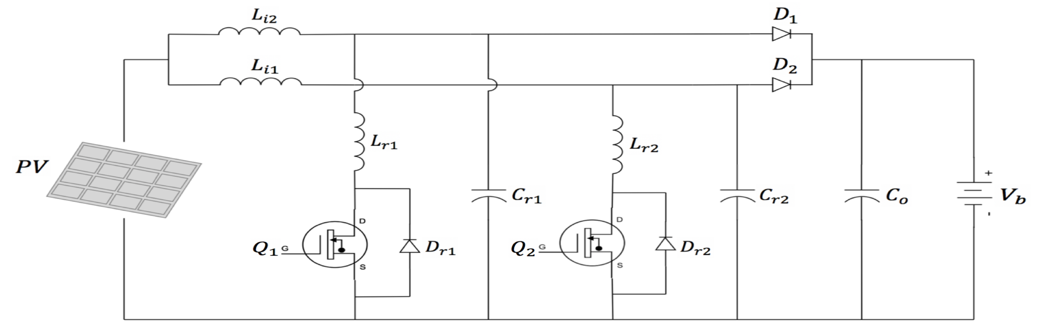
Figure 1 shows the schematic diagram of a two-stage parallel full-wave ZCS quasi-resonant converter utilized in this work. In this figure, L r 1 and L r 2 are the resonant inductors. Furthermore, C r 1 , C r 2 , L i 1 and L i 2 are the resonant capacitors and main inductors of the converter, respectively. The output capacitor is represented by C o . The switching power pole of the converter in Figure 1 is represented by the MOSFET switches Q 1 and Q 2 , along with Schottky diodes D 1 and D 2 . Diodes D r 1 and D r 2 represent the snubber diodes of switches Q 1 and Q 2 , respectively. The output voltage of the converter is represented by V b which feeds the battery.
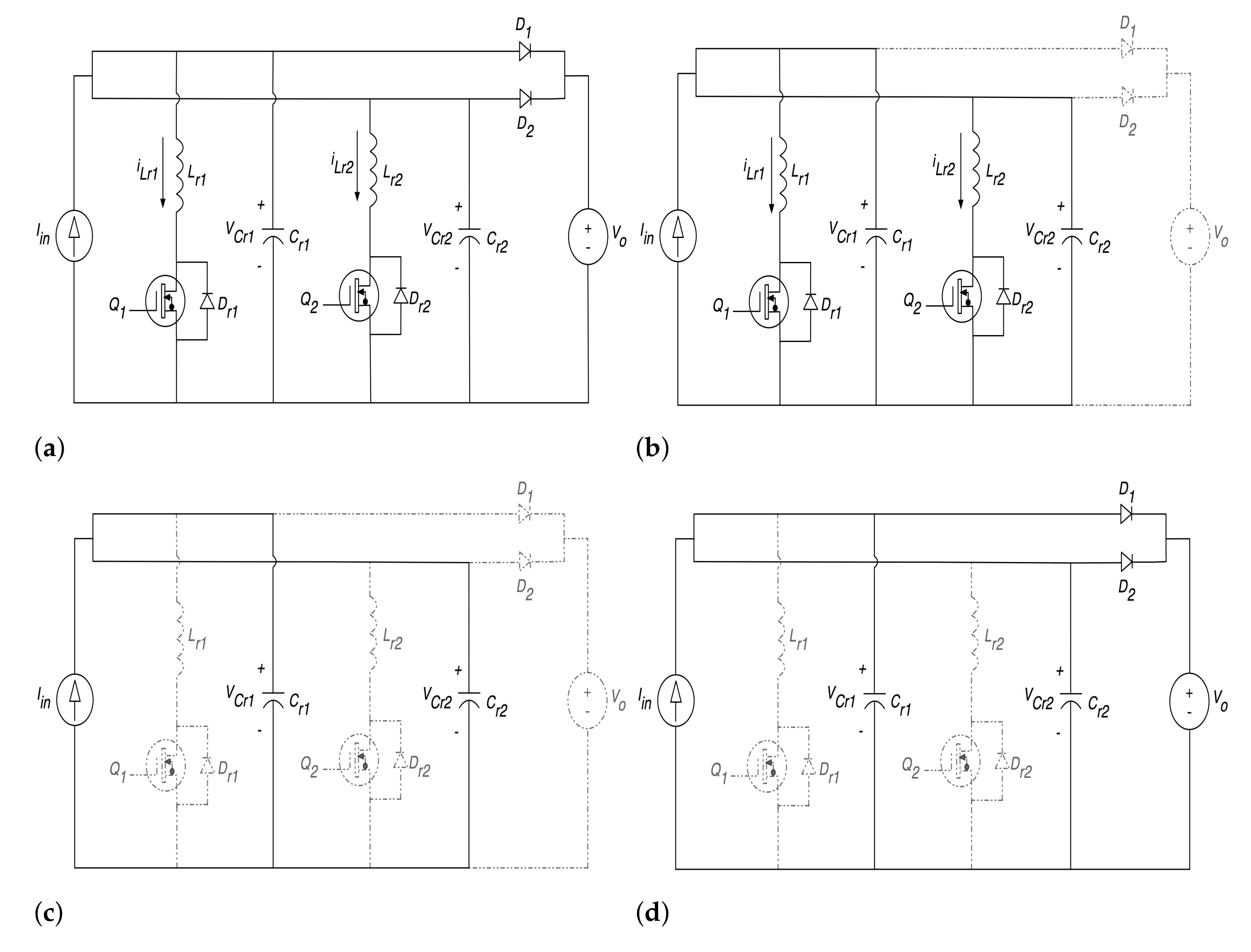
To simplify the analysis of the quasi-resonant converter without loss of generality, we assume the voltage drop across all semiconductor elements and diodes in the on-state is negligible. Further, the input current and output voltage ripples are not considered in the design. To satisfy the previous assumptions, the values of the inductors L i 1 and L i 2 along with the output capacitor C o are chosen to be high enough such that the voltage of output capacitor and the current through the inductors are constant DC values. Hence, inductors L i 1 and L i 2 as well as the PV module are modeled as a DC current source I i n . Similarly, the battery voltage together with the output capacitor C o are replaced by a DC voltage source V o as shown in Figure 2.
The converter utilized in this work has four modes of operation as shown in Figure 2. Derivation of the converter’s dynamics are presented in detail in this section. The initial state of switches Q 1 and Q 2 are considered to be off. Further, at t = 0 , diodes D 1 and D 2 are conducting.
Mode I ( t 0 t t 1 ) : In this mode of operation, both switches Q 1 and Q 2 are turned on at t = t 0 as shown in Figure 2a. The current through the resonant inductors starts to increase from zero until the sum of both currents reach the input current I i n . Using Kirchhoff’s circuit laws, we have
L r 1 d i L r 1 d t = L r 2 d i L r 2 d t = V o V C r 1 ( t ) = V C r 2 ( t ) = V o
where i L r 1 and i L r 2 are the currents of resonant inductors L r 1 and L r 2 , respectively. Further, V C r 1 and V C r 2 are the voltages across the resonant capacitors C r 1 and C r 2 , respectively. The initial values of the resonant inductors’ currents are assumed to be zero, hence we have
i L r 1 ( t ) = V o ( t t 0 ) L r 1 i L r 2 ( t ) = V o ( t t 0 ) L r 2 V C r 1 ( t ) = V C r 2 ( t ) = V o
Using (2), the currents i D 1 and i D 2 of both diodes D 1 and D 2 can be found as follows
i D 1 ( t ) = I i n 2 V o ( t t 0 ) L r 1 i D 2 ( t ) = I i n 2 V o ( t t 0 ) L r 2
Diodes D 1 and D 2 will become reverse-biased (off), at t = t 1 , when i L r 1 ( t 1 ) + i L r 2 ( t 1 ) = I i n or i D 1 ( t 1 ) = i D 2 ( t 1 ) = 0 . Hence, T 1 , the duration of Mode I can be obtained as follows
T 1 = t 1 t 0 = ( L r 2 + L r 1 ) I i n 2 V o
Multiplying both sides of (4) by ω r , we have
ω r T 1 = Z r I i n V o = α ,
where
ω r = 1 / L r 1 C r 1 Z r = L r 1 C r 1
which represents the time interval, T 1 , as α in radian.
Mode II ( t 1 t t 2 ) : The two auxiliary diodes D 1 and D 2 remain reverse biased (off) from the previous mode. Further, switches Q 1 and Q 2 continue to be on in this mode as shown in Figure 2b. This mode is mainly called the resonance mode, as the resonant components L r 1 , L r 2 , C r 1 and C r 2 are resonating at a resonant frequency of ω r . Using Kirchhoff’s circuit laws, we have
L r 1 d i L r 1 d t = V C r 1 L r 2 d i L r 2 d t = V C r 2 C r 1 d V C r 1 d t = C r 2 d V C r 2 d t = I i n i L r 1 ( t ) i L r 2 ( t )
By performing some algebraic manipulation to (7), I i n along with V C r 1 and V C r 2 can be found as
I i n = i L r 1 ( t ) + i L r 2 ( t ) V o Z r sin ω r ( t t 1 ) V C r 1 ( t ) = V C r 2 ( t ) = V o cos ω r ( t t 1 )
Each switch is connected to a series resonant inductor that is turned off at the second zero crossing of the currents, i L r 1 and i l r 2 . Both switches Q 1 and Q 2 are switched off under full-wave ZCS because of the resonant inductors L r 1 and L r 2 . In other words, Q 1 is turned off when i L r ( t 2 ) = 0 and Q 2 is turned off when i L r ( t 2 ) = 0 . This mode ends at t = t 2 , hence Mode II has a duration of T 2 , which is obtained as follows
T 2 = t 2 t 1 = sin 1 ( Z r I i n V o ) ω r .
By rearranging (9), we have
ω r T 2 = β ,
where the time interval T 2 can be expressed as β = 2 π sin 1 ( Z r I i n V o ) in radian.
Under full-wave operation, β should be between 1.5 π and 2 π . In this case, both switches Q 1 and Q 2 are turned off at the second zero crossing of the inductor current at t = t 2 , and this transitions to the next mode.
Mode III ( t 2 ≤ t ≤ t 3 ): In this mode of operation, the resonant capacitors, C r 1 and C r 2 , each continue to charge until reaching the value of the output voltage V o . The two auxiliary diodes D 1 and D 2 , as well as Q 1 and Q 2 , remain turned off in this mode as shown in Figure 2c. Similar to the previous modes, by manipulating the algebraic expressions and using Kirchhoff’s circuit laws, we have
i L r 1 ( t ) = i L r 2 ( t ) = 0 V C r 1 ( t ) = I i n ( t t 2 ) 2 C r 1 + V o cos β V C r 2 ( t ) = I i n ( t t 2 ) 2 C r 2 + V o cos β
This mode ends at t = t 3 , when the voltage of the resonant capacitors V C r 1 ( t 3 ) = V C r 2 ( t 3 ) = V o , hence resulting in D 1 and D 2 to start conducting (on). The duration of this mode, T 3 , is found as
T 3 = t 3 t 2 = 2 V o C r 1 C r 2 ( 1 cos β ) I i n ( C r 1 + C r 2 ) .
Multiplying ω r to both sides of (12), we obtain
ω r T 3 = γ ,
where the time interval T 3 is equivalent to γ = V o ( 1 cos β ) Z r I i n in r a d domain.
Mode IV ( t 3 t ): In mode 4, the switches Q 1 and Q 2 remain off, however, in this mode, diodes D 1 and D 2 are on as shown in Figure 2d. By applying Kirchhoff’s circuit, we have
i L r 1 ( t ) = i L r 2 ( t ) = 0 V C r 1 ( t ) = V C r 2 ( t ) = V o
Mode 4 transitions to the next switching cycle when the switches are turned back on.

3. Modeling of PV Module and Maximum Power Point Tracking Algorithm

This section describes the characteristics of the utilized PV module and the algorithm implemented to extract maximum voltage from the PV module.

3.1. Photo Voltaic Characteristics

The equivalent circuit of a PV cell is shown in Figure 3. The PV cell’s voltage, V, is used to obtain an expression for the output current, I, of the equivalent circuit [18,19]. The photo-current, I L , is a function of the cell’s irradiance and temperature.
The amount of solar energy harvested from the PV system is mainly influenced by the solar irradiance. As the irradiance decreases, the short circuit current decreases. Hence, the PV system generates higher power when the irradiance is high [20]. Figure 4 describes the P-V characteristics curve of the PV cell. The PV power curve increases with an increase in solar irradiance. The equations governing the V-I characteristic of the PV, based on the equivalent circuit shown in Figure 3, are given by
I = I L I D I s h I = I L I o [ e V + I R S n V T 1 ] V + I R s R p
where I is the cell current, n is the diode quality factor, V T is the thermal voltage of the cell, R s is the series resistance and R p is the shunt resistance [21].

3.2. Maximum Power Point Tracking Algorithm

The MPPT converter applies current control to track the maximum power operating point and obtain the voltage at maximum power point. The MPPT algorithm utilized in this work is P&O technique, which is usually used to alter the duty cycle to obtain the maximum power; however, to ensure the functionality of both soft-switching technique and MPPT, the current is being altered by the proposed P&O algorithm in this work as shown in Figure 5.
The P-V characteristics curve is different for each specific irradiance. Using P&O, the value of the voltage at maximum power point ( V m p p ) is obtained as shown in Figure 4. As the irradiance changes, V m p p , which is the peak voltage at maximum power, is extracted.

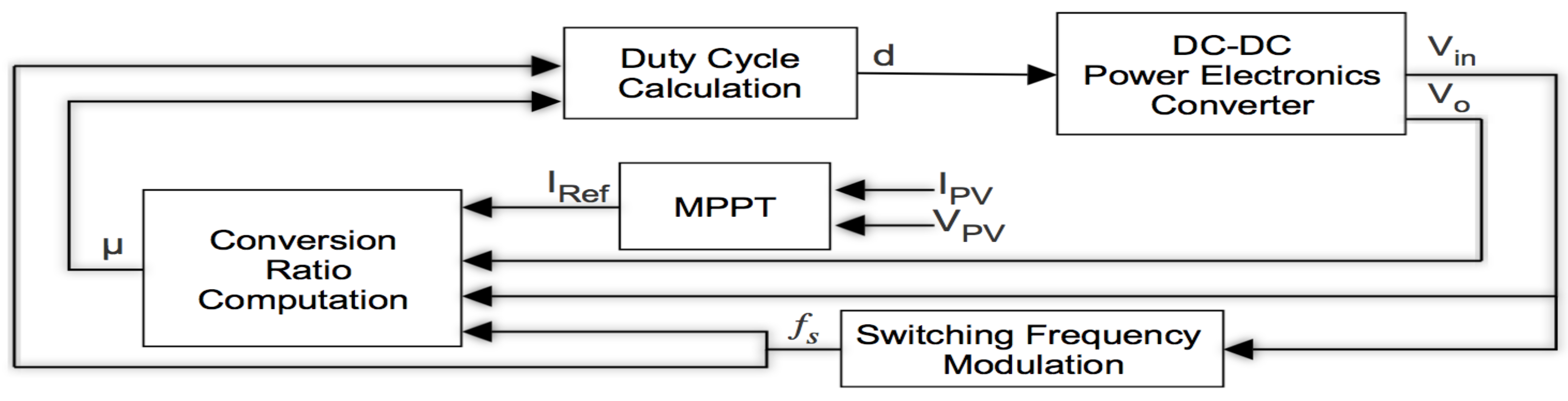
4. Conversion Ratio and Controller Design

In this section an equation representing the conversion ratio of the utilized two-stage parallel full-wave ZCS quasi resonant boost converter is derived. The obtained conversion ratio reveals that both average values of the converter’s current and voltage are dependent and controlled by the resonant components of the soft-switching converter. The conversion ratio can be derived as follows
μ = i 1 ( t ) T s i 2 ( t ) T s ,
where i 2 ( t ) and i 1 ( t ) are the output and input currents of the converter, respectively. The input current can be found, using Kirchoff’s current law, as the sum of the resonant inductors’ current and the output current. The conversion ratio μ of the proposed converter can be calculated as
μ = i L r ( t ) T s + I o I o = 1 + i L r ( t ) T s I o .
where T s represents the switching period and i L r is the sum of i L r 1 and i L r 2 .
The average current value of both resonant inductors i L r ( t ) T s can be calculated by dividing the total charge passing through the inductors during the resonance phase over the total switching period as follows
i L r ( t ) T s = Δ q T s ,
where Δ q = q 1 + q 2 . The charges of the inductors during the resonance phase Mode I and Mode II are represented by q 1 and q 2 , respectively. For Mode I, q 1 is found as
q 1 = t 0 t 1 i L r ( t ) d t .
Substituting i l r from (2) and applying some algebraic manipulations, we obtain the following
q 1 = 0 α ω r V o τ L r 1 d τ = α I i n 2 ω r ,
where τ = t t 0 and L r 1 = L r 2 . Further, by using (8), q 2 in Mode II can be calculated as
q 2 = α ω r α + β ω r [ I i n + V o Z r sin ω r ( τ α ) ] d τ = I i n β ω r + V o C r 1 V c 1 C r 1 ,
where V c 1 is the voltage across the resonant capacitor C r 1 at the end of mode II, which is equal to the voltage across resonant capacitor C r 2 . The voltage across the resonant capacitors at t = t 2 can be found as
V c 1 = V o 1 ( Z r I i n V o ) 2 .
Substituting (20) and (21) into (18), we have
i L r ( t ) T s = F 2 π α I i n 2 + β I i n + V o Z r ( 1 1 J s 2 ) .
Furthermore, by substituting (23) into (17), the conversion ratio μ can be obtained as
μ = 1 1 F 2 π 1 2 J s + 2 π sin 1 J s + 1 J s ( 1 1 J s 2 ) ,
where J s and F are defined follows
J s = Z r I i n V o F = f s f r
and f r and f s are the resonant and switching frequencies, respectively.
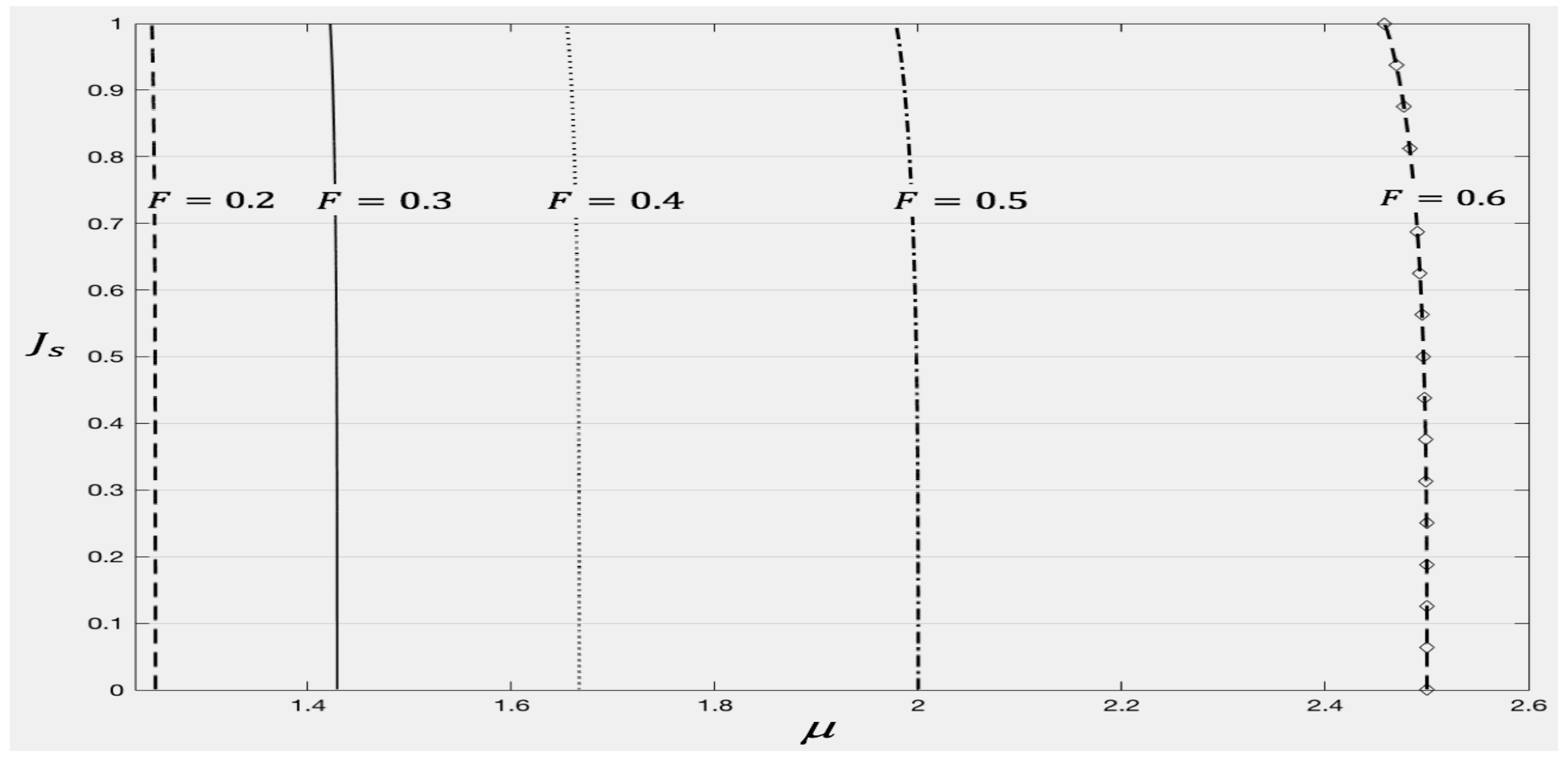
The variation of the conversion ratio μ in terms of F and J s is illustrated in Figure 6. From this figure, it is evident that the normalized frequency F impacts μ significantly. In the proposed control strategy, the resonant frequency f r is fixed; hence F is varied when the switching frequency f s is changed. A control strategy is designed based on the normalized frequency property, by controlling the switching frequency of the switches of the utilized converter to ensure a robust output voltage.
At the steady-state, the voltages of the input inductors of the converter have an average value of zero. To derive an expression for the voltage gain of the utilized converter, the voltages of the input inductors during resonance mode are equated to the input inductors’ voltage for the remaining time at steady-state. The expression is found as
V o V i n = 1 ( f s f r ) ,
where V i n is the input voltage of the converter. In addition to that, the on-time duration, t o n , of both switches is found by adding the on times of the switches in Mode I and Mode II. The on-time duration is expressed as
t o n = T 1 + T 2 .
Equations (24) and (
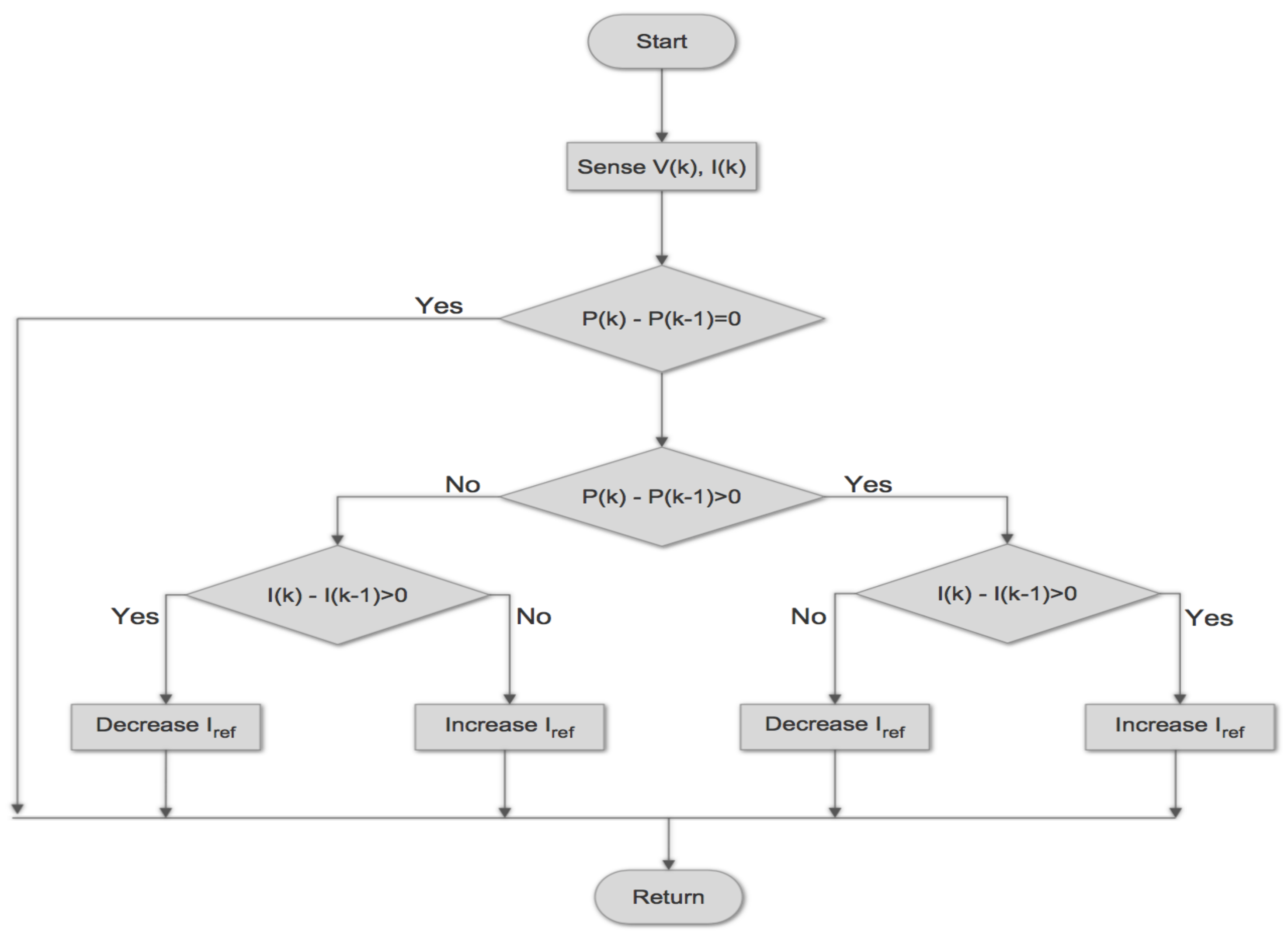
26) are the basis of the proposed control strategy and switching regime. Furthermore, the current obtained from the MPPT algorithm block is used to ensure that the input voltage of the converter is at the maximum power point voltage. The reference current is given by
I R E F = I M P P T I M ,
where I M P P T is the value of the current extracted from MPPT and I M is the measured input current.
Figure 7 illustrates the proposed control strategy and switching regime that controls and regulates the output voltage to charge a battery load at maximum input voltage through soft switching technique.

5. Design Procedure of the Converter

5.1. Switch-Mode Battery Charger Design

In this section, the practical limitations to ensure the proper operation of the converter for a typical battery charging system are discussed and considered for selecting the numerical values of the circuit components of the utilized two-stage parallel full-wave ZCS quasi resonant converter. The load connected to the output of the converter impacts the circuit dynamics. Furthermore, integrating a lithium–ion battery as a load is challenging. The battery experiences both source and sink current capabilities; however, in standalone controllers, only sink current capabilities are experienced. For this reason, to avoid draining the battery, the reverse discharge is reduced by decreasing the run-time. In this work, the exponential zone voltage and cut-off voltage are adjusted. In addition to that, the appropriate filter components are selected for the utilized converter to behave as a battery charger. The output current of the converter should have a high value to decrease the thermal dissipation from the battery, hence increasing the efficiency of the charger and obtaining maximum charging current. The charge current rate is limited by the free-wheeling diode and switching devices. In this case, the maximum charge current rate in the battery design is 1–1.5 Ah.
The time to fully charge the battery is approximately 20 min. The charging time can be made faster if the output current is high, but increasing the output current negatively impacts the battery’s health in the long-term. The state of charge, S O C , can be calculated as
S O C = ( Q r Q r a t e ) * 100
where Q r a t e is rated capacity of the battery and Q r is the capacity remaining in the battery. Further, the time to fully charge the battery, T c , is given by
T c = C a p a c i t y ( A h ) C u r r e n t ( A ) ( 1.2 )
It should be noted that we have considered a 1.2 ratio in (30) to account for 20% efficiency loss.
In this work, a lithium–ion battery is considered in the design. The maximum charge voltage is 30 V with a capacity of 1 Ah.

5.2. Converter Design

The maximum power point voltage of the PV system is taken to be 17.2 V. The irradiance is changed to specific values to consider the intermittent nature of the PV system under different irradiance levels. Table 1 lists all design parameters considered in the proposed system.
Referring back to Figure 1, the resonant components, at steady state, are connected in parallel to the input source and output of the converter. The converters’ main filter components do not fully discharge, hence experiencing peak-to-peak ripple current Δ i L during steady state oscillation. In the design of the filter components of the converter, the current ripple is considered to be 5% and the allowable voltage ripple is taken as 15%. The values of the filter capacitor and inductors can be calculated from [22] as
L i 1 = L i 2 = ( V b V i n , m i n ) ( 1 t o n ) Δ i L
C o = i c t o n Δ V o
where i c is output capacitor current and Δ V o is the output voltage ripple.
The size of the resonant filters are selected to ensure the functionality of soft switching in the utilized converter. The currents through the resonant inductors in each switching cycle should reach zero. Therefore, from Mode II, referring to (9), we should have the following condition
Z r I i n , m i n V o < 1 .
In addition to that, to limit the charging current ripple and output voltage ripple, three considerations are taken into account. First, the resonant tank values, i.e., the resonant capacitors and resonant inductors are selected to be much smaller than the values of the converter’s capacitor and inductors. Further, J s from Equation (9) should satisfy the condition of Equation (33). J s is considered to be lower than the constant value 1, hence the value of Z r is selected to be lower than 4.68 Ω .

6. Evaluation Results and Analysis

A test system consisting of the soft-switching topology along with the proposed switching regime and control strategy is implemented using MATLAB Simulink Simscape and its real-time workshop on the DS1103 PPC controller mounted in a dSPACE expansion box. The converter is built using predefined circuit parameters tabulated in Table 1. The performance of the system is then evaluated through several experiments under various scenarios.
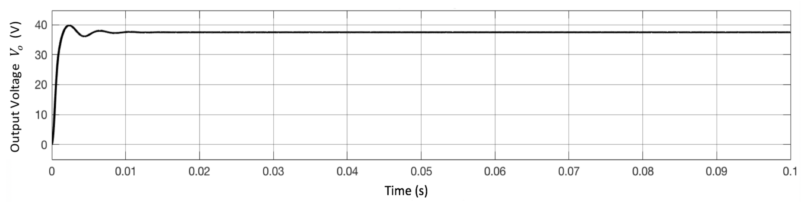
Figure 8 shows the output voltage of the converter without using the proposed controller. The input voltage is varied to check the behavior of the system. Figure 8 reveals that the output voltage does not reach the desired value. In this case, the output voltage reaches an undesirable value of 38 V.
To improve the results obtained from Figure 8, the proposed switching regime and control strategy presented in Section 4 are utilized to overcome irregularities and changes experienced by the converter. The proposed topology maintains and regulates the output voltage of the converter at 30 V DC, regardless of any changes experienced at the input of the converter, due to weather conditions and changes in irradiance levels.
The irradiance of the PV is set to 1000 W/m 2 ; 
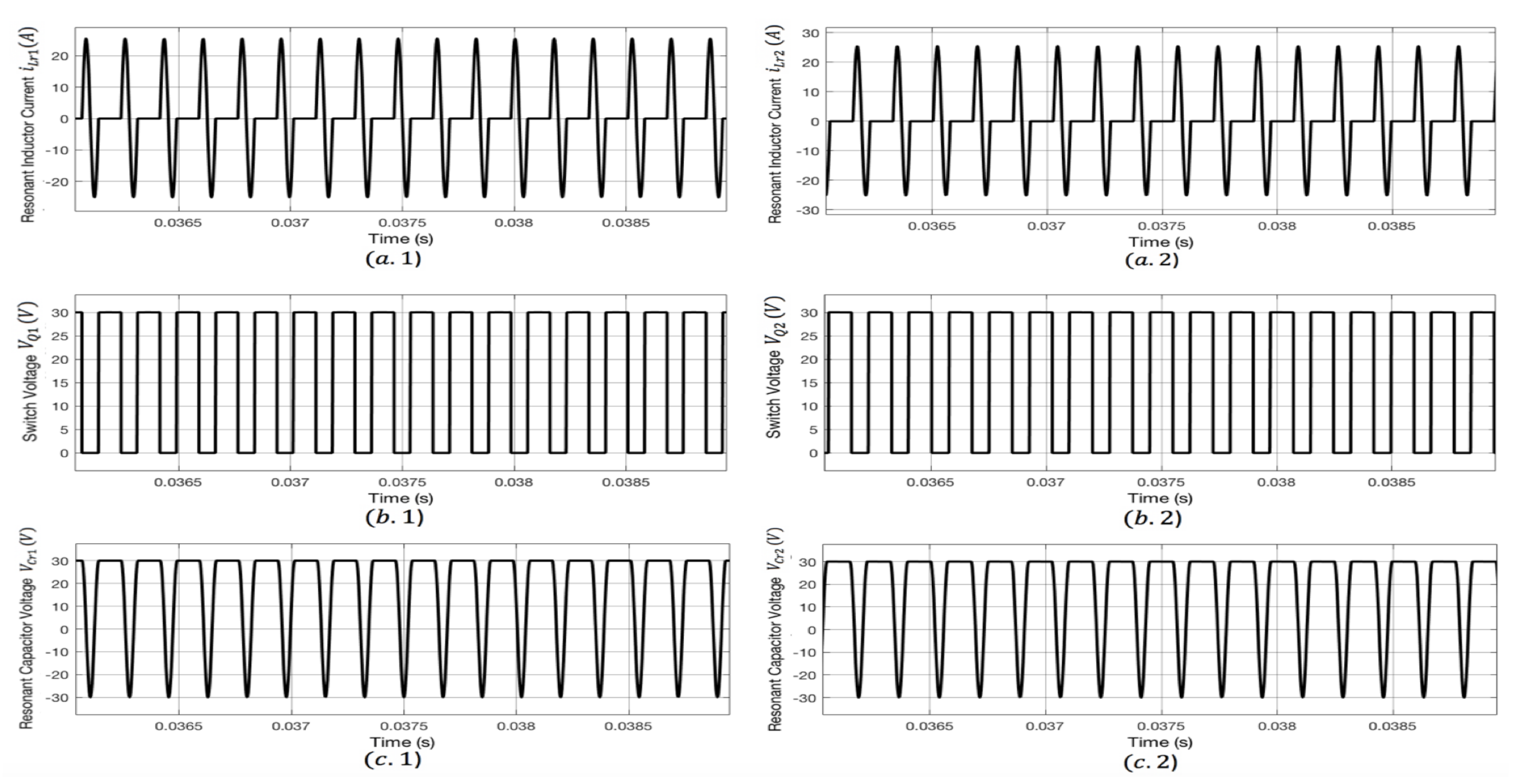
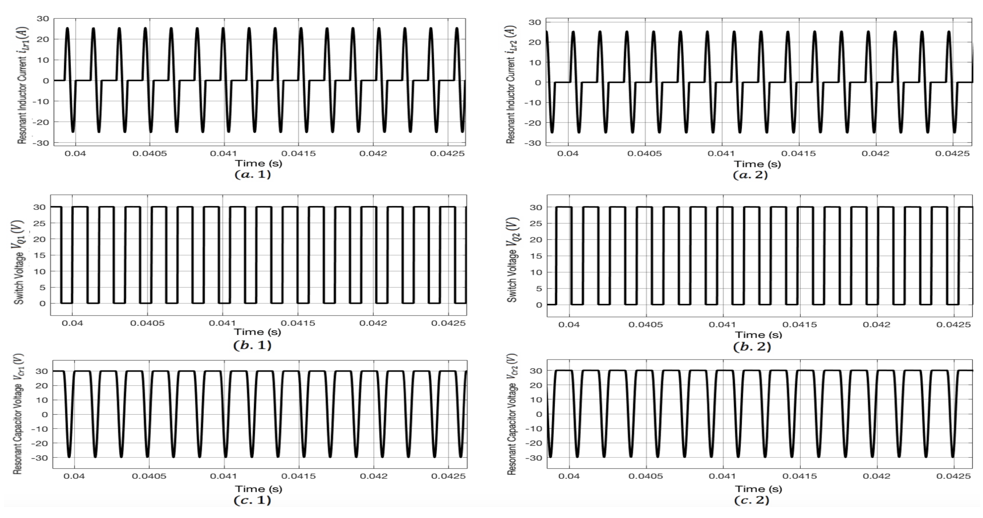
Figure 9 shows the soft-switching functionality of the implemented two-stage parallel full-wave ZCS quasi resonant boost converter. It is evident from 
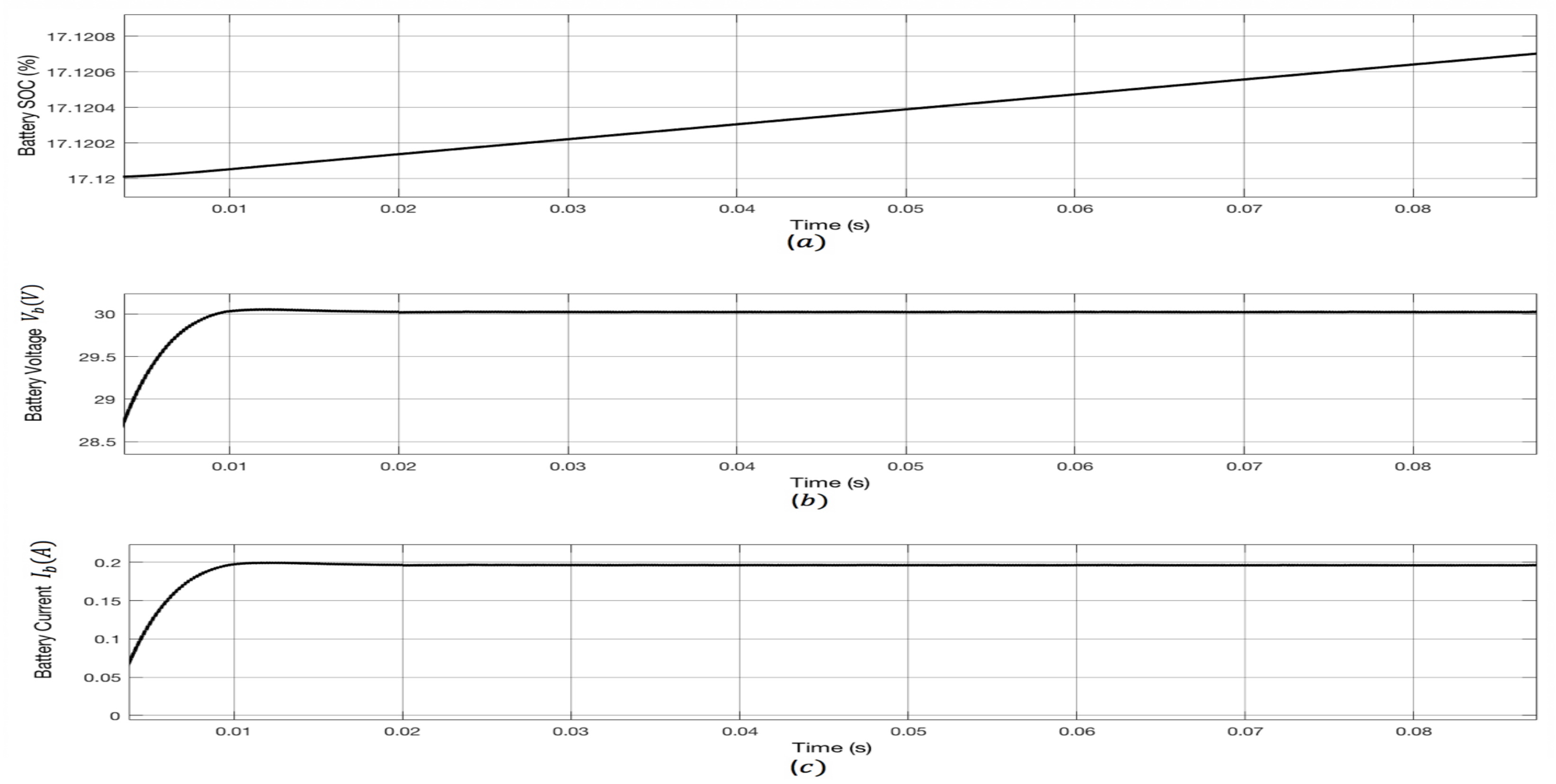
Figure 9 that the voltage of both switches is zero or in other words turned off at the second zero crossing of the resonant inductors’ currents. The waveforms of both switch voltages and resonant inductor currents confirm the functionality of the DC–DC boost converter at full-wave soft-switching. Moreover, 
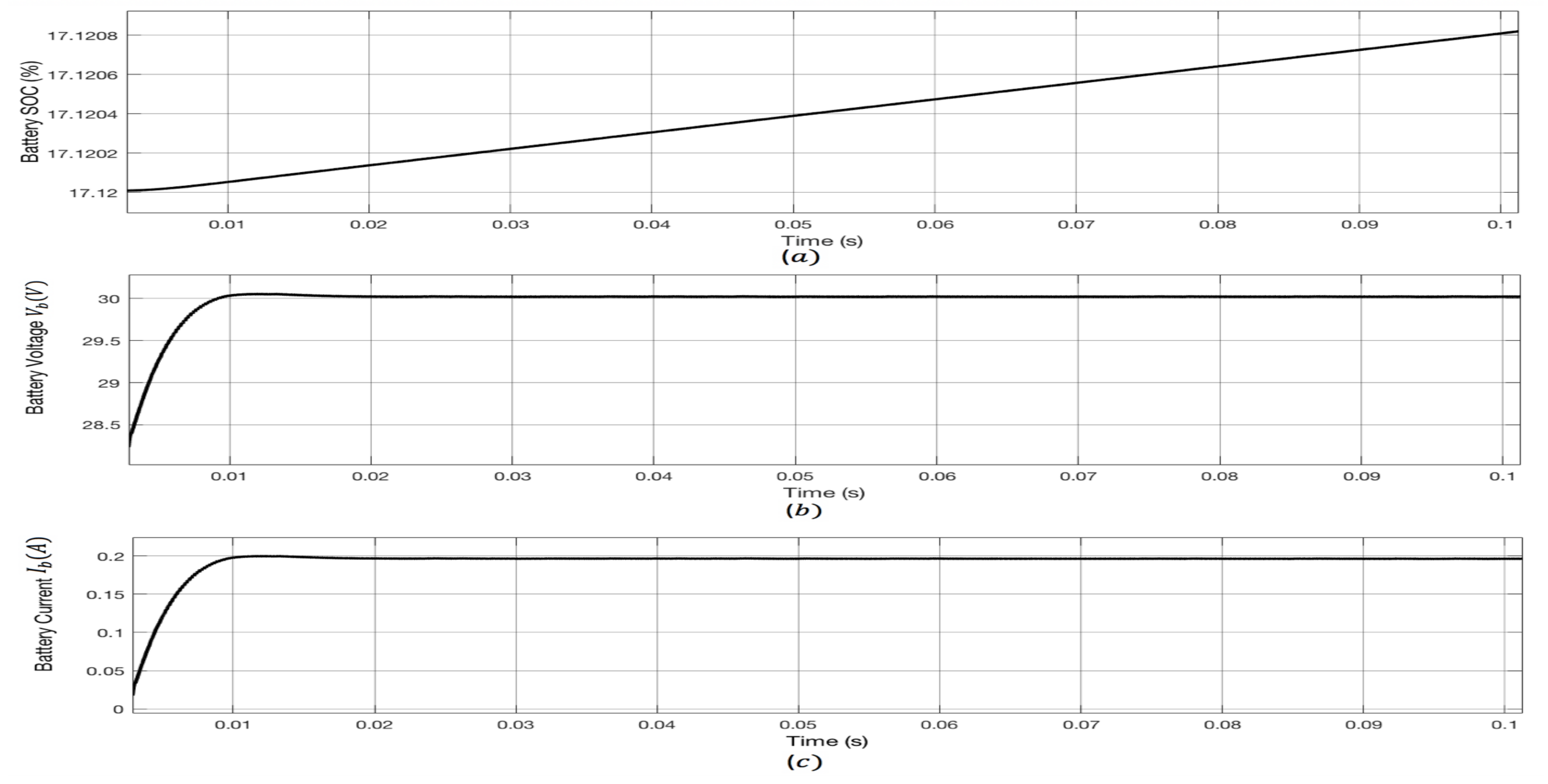
Figure 10 shows that the converter is able to reach the desired value of 30 V at the output, along with an increase in the battery S O C , when the irradiance is set to 1000 W/m 2 .
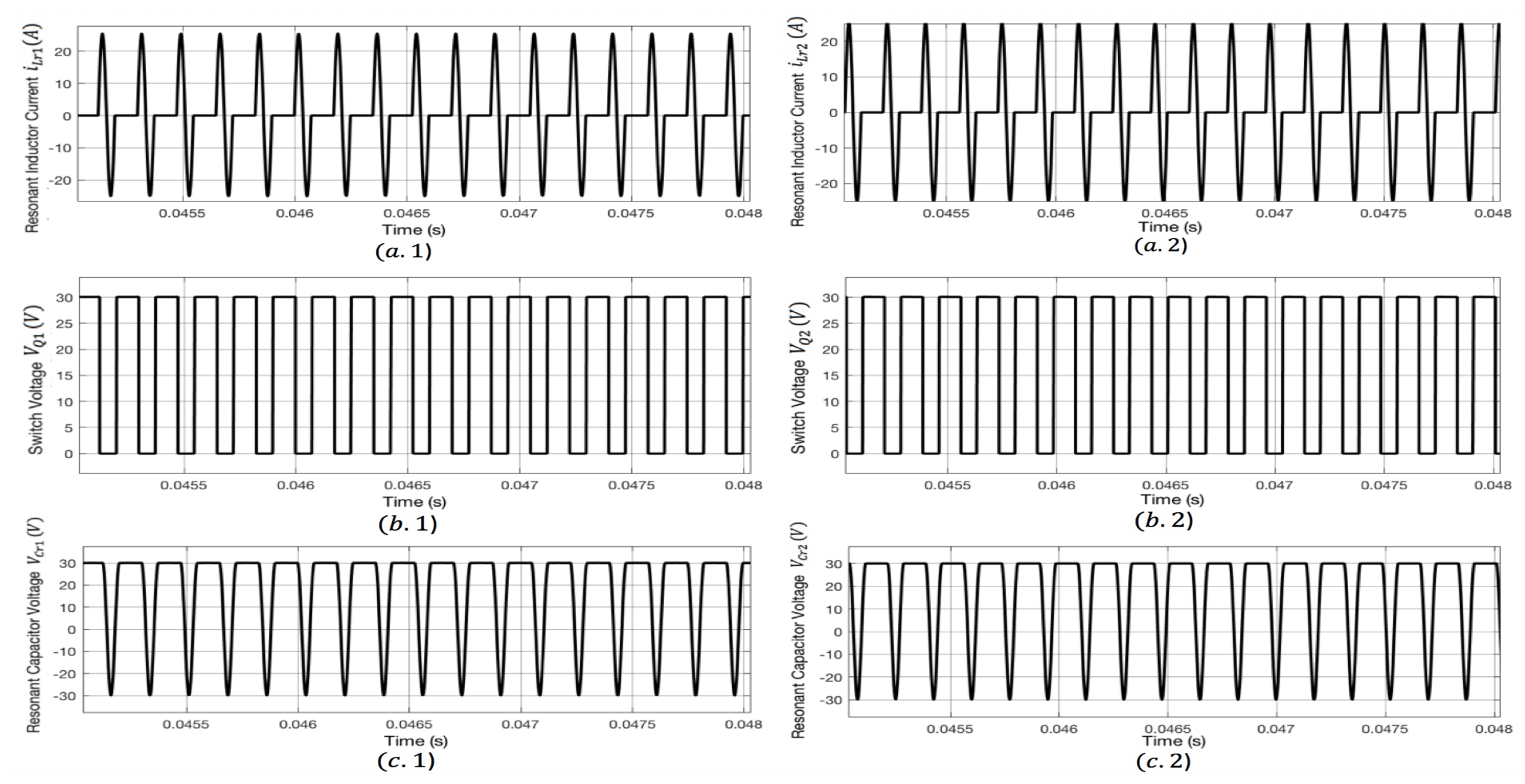
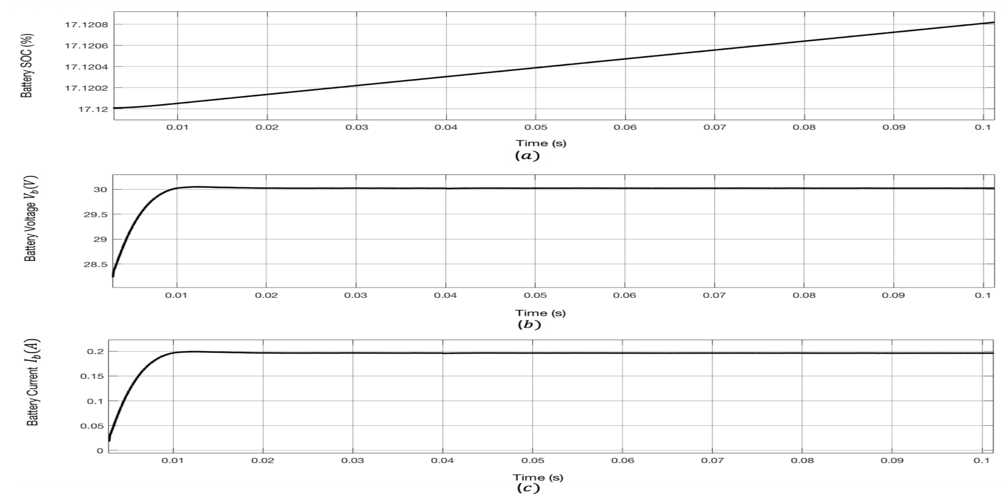
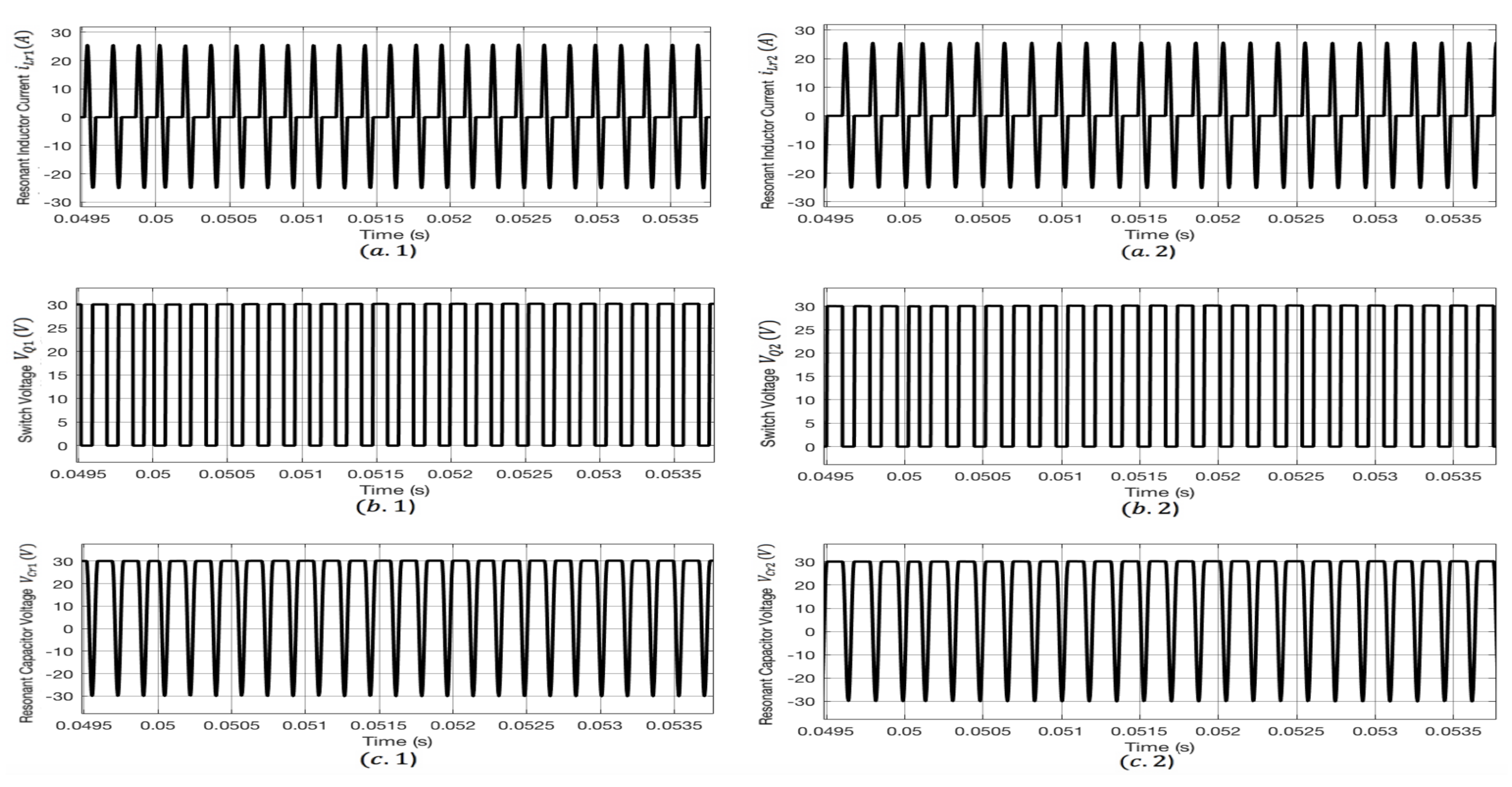
Furthermore, the irradiance of the PV system is changed to evaluate the behavior of the proposed topology. Figure 11 and Figure 12 show the corresponding waveforms of the converter at an irradiance value of 950 W/m 2 . It is evident from both figures that the desired output voltage of 30 V is reached using full-wave ZCS soft-switching to charge the battery load. Similarly, Figure 13 and Figure 14 validate the functionality of the utilized converter along with the proposed controller at an irradiance of 900 W/m 2 .
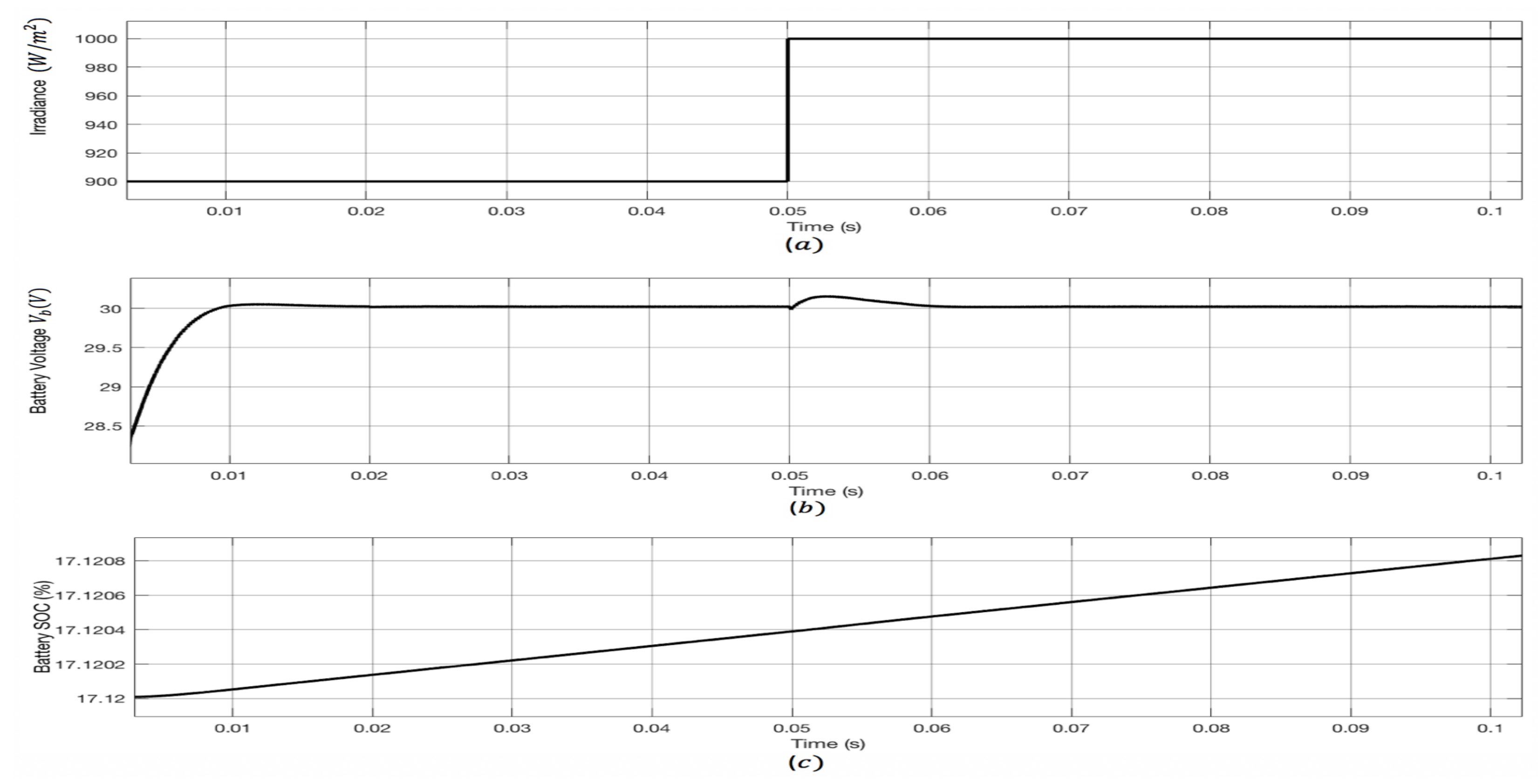
Due to the intermittent nature of the PV system, it is vital to evaluate the capability of the proposed topology to sudden changes in the irradiance. In this case, the irradiance is change from 900 W/m 2 to 1000 W/m 2 after 0.05 s. When the irradiance is altered, the switching still occurs at the second zero crossing of the inductor currents as shown in Figure 15. Further, Figure 16 shows that the converter is able to effectively handle the sudden change of irradiance while maintaining the output voltage at 30 V. The proposed controller successfully forces the voltage back to 30 V after 0.05 s.
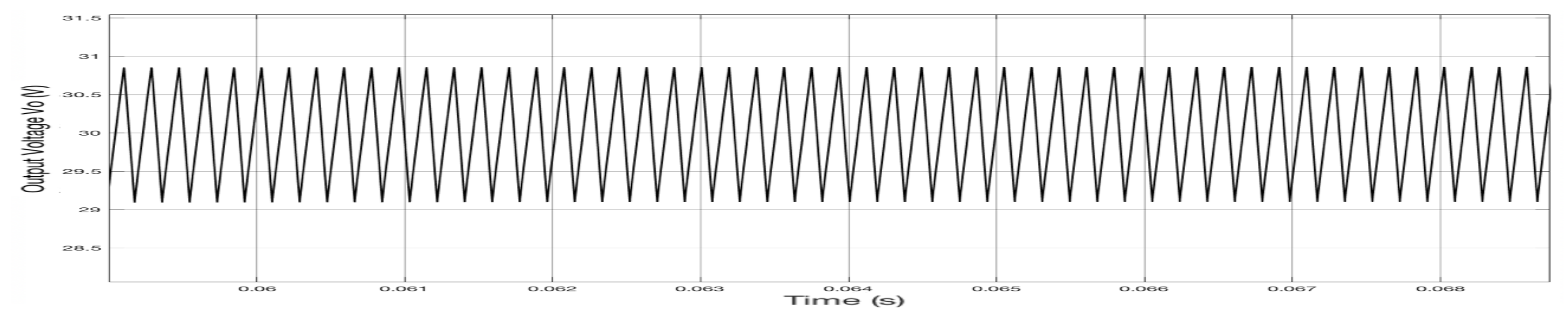
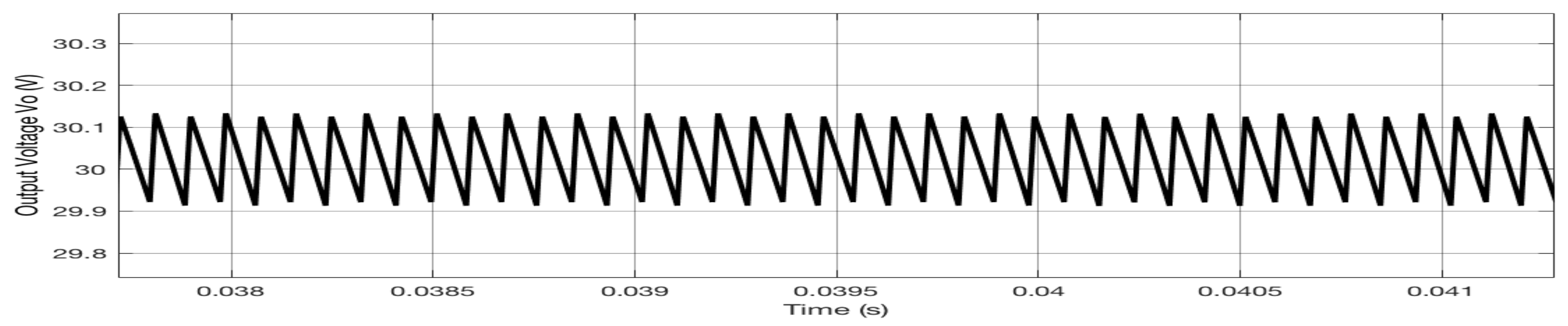
Due to the parallel topology adopted in this work, the ripple of the output voltage is reduced significantly. From Figure 17, it is evident that the output voltage ripple is approximately 1.5 V without interleaving boost converter; however, for the utilized two-stage parallel topology, the output voltage ripple is dropped down to 0.2 V, as shown in Figure 18. Furthermore, 
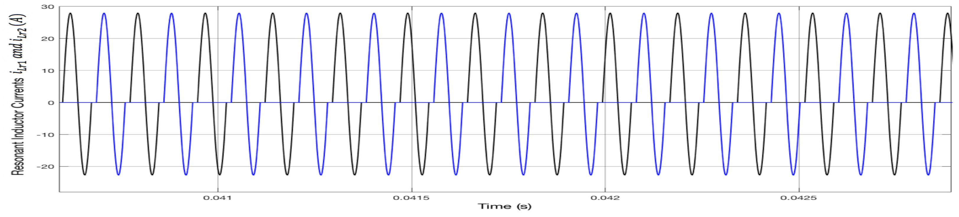
Figure 19 shows the currents of the resonant inductors L r 1 and L r 2 . The resonant inductors’ currents increase and decrease sinuously according to the gate signals.

7. Conclusions

In this work, a two-stage parallel full-wave ZCS quasi-resonant boost converter along with MPPT and frequency-modulated control strategy was proposed for charging a battery load from a PV system. The maximum voltage extracted from the PV system is stepped-up using two parallel boost converters with soft switching operation. The results show the performance and effectiveness of the proposed control strategy and switching regime under different irradiance levels and intermittent behavior of PV system to regulate the output voltage at a desired constant DC voltage for charging the battery load.

Author Contributions

Conceptualization, R.S. and R.G.; Methodology, R.S. and R.G.; Software, R.S. and R.G.; Validation, R.S. and P.F.; Formal analysis, R.S. and R.G.; Investigation, R.S. and R.G.; Resources, R.S.; Writing—original draft preparation, R.S. and R.G.; Writing—review and editing, R.S. and P.F.; Supervision, R.S.; Project administration, R.S.; Funding acquisition, none. All authors have read and agreed to the published version of the manuscript.

Funding

This research received no external funding.

Institutional Review Board Statement

Not applicable.

Informed Consent Statement

Not applicable.

Data Availability Statement

The data presented in this study are available on request from the corresponding author.

Conflicts of Interest

The authors declare no conflict of interest.

Abbreviations

The following abbreviations are used in this manuscript:
MOSFETMetal Oxide Semiconductor Field Effect Transistor
MPPTMaximum Power Point Tracking
P&OPerturb and Observe
PVPhotovoltaic
PWMPulse Width Modulation
S O C State Of the Charge
ZCSZero Current Switching
ZVSZero Voltage Switching

References

  1. Zacharias, A.M.; Devaprakash, T.R. Modeling and simulation of photovoltaic system with soft switching SEPIC converter. In Proceedings of the 2014 Annual International Conference on Emerging Research Areas: Magnetics, Machines and Drives (AICERA/iCMMD), Kottayam, India, 24–26 July 2014; pp. 1–6. [Google Scholar]
  2. Latifi, M.; Sabzehgar, R.; Rasouli, M.; Fajri, P. Active and reactive power compensation using a pev-based three-level capacitor clamped inverter. In Proceedings of the 2019 IEEE Texas Power and Energy Conference (TPEC), College Station, TX, USA, 7–8 February 2019; pp. 1–6. [Google Scholar]
  3. Sabzehgar, R.; Roshan, Y.M.; Fajri, P. Modelling and sliding-mode control of a single-phase single-stage converter with application to plug-in electric vehicles. IET Power Electron. 2019, 12, 620–626. [Google Scholar] [CrossRef]
  4. Tiwari, S.; Sabzehgar, R.; Rasouli, M. Short term solar irradiance forecast based on image processing and cloud motion detection. In Proceedings of the 2019 IEEE Texas Power and Energy Conference (TPEC), College Station, TX, USA, 7–8 February 2019; pp. 1–6. [Google Scholar]
  5. Sabzehgar, R.; Amirhosseini, D.Z.; Rasouli, M. Solar power forecast for a residential smart microgrid based on numerical weather predictions using artificial intelligence methods. J. Build. Eng. 2020, 32, 101629. [Google Scholar] [CrossRef]
  6. Farhangi, B.; Farhangi, S. Comparison of z-source and boost-buck inverter topologies as a single phase transformer-less photovoltaic grid-connected power conditioner. In Proceedings of the 2006 37th IEEE Power Electronics Specialists Conference, Jeju, Korea, 18–22 June 2006; pp. 1–6. [Google Scholar]
  7. Behjati, H.; Davoudi, A. A Multiple-Input Multiple-Output DC–DC Converter. IEEE Trans. Ind. Appl. 2013, 49, 1464–1479. [Google Scholar] [CrossRef]
  8. Keyhani, H.; Toliyat, H.A. A new generation of buck-boost resonant AC-link DC-DC converters. In Proceedings of the 2013 Twenty-Eighth Annual IEEE Applied Power Electronics Conference and Exposition (APEC), Long Beach, CA, USA, 17–21 March 2013; pp. 1383–1390. [Google Scholar] [CrossRef]
  9. Pavlovsky, M.; Guidi, G.; Kawamura, A. Buck/boost DC–DC converter topology with soft switching in the whole operating region. IEEE Trans. Power Electron. 2013, 29, 851–862. [Google Scholar] [CrossRef]
  10. Kiran, B.R.; Ezhilarasi, G. Design and analysis of soft-switched Buck-Boost Converter for PV applications. In Proceedings of the 2015 Annual IEEE India Conference (INDICON), New Delhi, India, 17–20 December 2015; pp. 1–5. [Google Scholar]
  11. Zhang, Y.; Sen, P.C. A new soft-switching technique for buck, boost, and buck-boost converters. IEEE Trans. Ind. Appl. 2003, 39, 1775–1782. [Google Scholar] [CrossRef]
  12. Goryashin, N.N.; Solomatova, A.S. Analysis of MOSFET operating in half-wave zero-current switching quasi-resonant converter. In Proceedings of the International Conference and Seminar of Young Specialists on Micro/Nanotechnologies and Electron Devices, Altai, Russia, 2–6 July 2012; pp. 333–337. [Google Scholar]
  13. Lakshminarasamma, N.; Masihuzzaman, M.; Ramanarayanan, V. Steady-State Stability of Current-Mode Active-Clamp ZVS DC–DC Converters. IEEE Trans. Power Electron. 2011, 26, 1295–1304. [Google Scholar] [CrossRef]
  14. Jabbari, M.; Farzanehfard, H. New Resonant Step-Down/Up Converters. IEEE Trans. Power Electron. 2010, 25, 249–256. [Google Scholar] [CrossRef]
  15. Hsieh, G.C.; Wang, C.M. ZCS-PWM full-wave boost rectifier with unity power factor and low conduction losses. IEEE Trans. Ind. Electron. 1999, 46, 768–779. [Google Scholar] [CrossRef]
  16. Lin, B.; Wu, R.; Chao, C.; Chiang, Y. Interleaved double series resonant converter. In Proceedings of the 2011 6th IEEE Conference on Industrial Electronics and Applications, Beijing, China, 21–23 June 2011; pp. 1815–1820. [Google Scholar] [CrossRef]
  17. Özdemir, G.; Yildiz, A.B. Time-domain analysis of full-wave quasi-resonant zero-current switching buck converter by modified nodal analysis. In Proceedings of the 2018 5th International Conference on Electrical and Electronic Engineering (ICEEE), Istanbul, Turkey, 3–5 May 2018; pp. 23–26. [Google Scholar]
  18. De Blas, M.; Torres, J.; Prieto, E.; Garcıa, A. Selecting a suitable model for characterizing photovoltaic devices. Renew. Energy 2002, 25, 371–380. [Google Scholar] [CrossRef]
  19. Walker, G.R. Evaluating MPPT converter topologies using a Matlab PV model. Aust. J. Electr. Electron. Eng. 2001, 21, 49–55. [Google Scholar]
  20. Krishan, R.; Sood, Y.R.; Kumar, B.U. The simulation and design for analysis of photovoltaic system based on MATLAB. In Proceedings of the 2013 International Conference on Energy Efficient Technologies for Sustainability, Nagercoil, India, 10–12 April 2013; pp. 647–651. [Google Scholar]
  21. Tan, C.W.; Green, T.C.; Hernandez-Aramburo, C.A. Analysis of perturb and observe maximum power point tracking algorithm for photovoltaic applications. In Proceedings of the 2008 IEEE 2nd International Power and Energy Conference, Johor Bahru, Malaysia, 1–3 December 2008; pp. 237–242. [Google Scholar]
  22. Mohan, N. Power Electronics: A First Course; John Wiley & Sons: Hoboken, NJ, USA, 2012; Volume 5774, p. 7030. ISBN 978-1-118-07480-0. [Google Scholar]
Figure 1. Two-stage parallel boost converter for PV-based charging system.
Electricity 03 00009 g001
Figure 2. Two-stage parallel full-wave ZCS quasi-resonant boost converter operation modes: (a) Mode I; (b) Mode II; (c) Mode III; (d) Mode IV. The parts of circuit that are not contributing in each mode of operation have been faded out with dashed line.
Electricity 03 00009 g002
Figure 3. Equivalent circuit of PV cell.
Electricity 03 00009 g003
Figure 4. The impact of solar irradiance on P-V characteristics.
Electricity 03 00009 g004
Figure 5. MPPT—perturb and observe current control.
Electricity 03 00009 g005
Figure 6. Characteristics of the utilized two-stage parallel full-wave ZCS quasi-resonant boost converter.
Electricity 03 00009 g006
Figure 7. The proposed control strategy and switching regime with MPPT implementation for the two-stage parallel full-wave ZCS quasi-resonant boost converter.
Electricity 03 00009 g007
Figure 8. Output voltage without controller.
Electricity 03 00009 g008
Figure 9. Waveforms for the converter along with the proposed control strategy and switching regime when irradiance = 1000 W/m 2 : (a) resonant inductor current i l r 1 and i l r 2 ; (b) switch voltage V Q 1 and V Q 2 ; (c) resonant capacitor voltage V C r 1 and V C r 2 .
Electricity 03 00009 g009
Figure 10. Waveforms for the battery load with the nominal voltage of 24 V and irradiance of 1000 W/m 2 : (a) battery S O C ; (b) battery voltage V b ; (c) battery current I b .
Electricity 03 00009 g010
Figure 11. Waveforms for the converter along with the proposed control strategy and switching regime when irradiance = 950 W/m 2 : (a) resonant inductor current i l r 1 and i l r 2 ; (b) switch voltage V Q 1 and V Q 2 ; (c) resonant capacitor voltage V C r 1 and V C r 2 .
Electricity 03 00009 g011
Figure 12. Waveforms for the battery load with the nominal voltage of 24 V and irradiance of 950 W/m 2 : (a) battery S O C ; (b) battery voltage V b ; (c) battery current I b .
Electricity 03 00009 g012
Figure 13. Waveforms for the converter along with the proposed control strategy and switching regime when irradiance = 900 W/m 2 : (a) resonant inductor current i l r 1 and i l r 2 ; (b) switch voltage V Q 1 and V Q 2 ; (c) resonant capacitor voltage V C r 1 and V C r 2 .
Electricity 03 00009 g013
Figure 14. Waveforms for the battery load with the nominal voltage of 24 V and irradiance of 900 W/m 2 : (a) battery S O C ; (b) battery voltage V b ; (c) battery current I b .
Electricity 03 00009 g014
Figure 15. Waveforms for the converter along with the proposed control strategy and switching regime when irradiance is changed from 900 to 1000 W/m 2 : (a) resonant inductor current i L r 1 and i l r 2 ; (b) switch voltage V Q 1 and V Q 2 ; (c) resonant capacitor voltage V C r 1 and V C r 2 .
Electricity 03 00009 g015
Figure 16. Waveforms for the battery load with the nominal voltage of 24 V with sudden change of irradiance from 900 to 1000 W/m 2 : (a) irradiance W/m 2 ; (b) battery voltage V b ; (c) battery S O C .
Electricity 03 00009 g016
Figure 17. Output voltage ripple with the single-stage resonant boost converter.
Electricity 03 00009 g017
Figure 18. Output voltage ripple with the utilized two-stage parallel resonant boost converter.
Electricity 03 00009 g018
Figure 19. The current waveform passing through L r 1 (blue) and L r 2 (black).
Electricity 03 00009 g019
Table 1. Converter design parameters.
ParameterSymbolValueUnit
Minimum Input Current I i n , m i n 5A
Maximum Input Current I i n , m a x 6.4 A
Output Capacitor C o 120 μ F
Input Inductor 1 L i 1 25mH
Input Inductor 2 L i 2 25mH
Resonant Inductor 1 L r 1 14 μ H
Resonant Inductor 2 L r 2 14 μ H
Resonant Capacitor 1 C r 1 10 μ F
Resonant Capacitor 2 C r 2 10 μ F
Publisher’s Note: MDPI stays neutral with regard to jurisdictional claims in published maps and institutional affiliations.

