
Proceeding Paper

Bi-Based Perovskite Materials for High-Sensitivity Gamma Ray Detection †

by
Paramesh Chandra
and
Swapan K. Mandal
*
Department of Physics, Visva-Bharati, Santiniketan 731 235, India
*
Author to whom correspondence should be addressed.
Presented at the 4th International Online Conference on Materials, 3–6 November 2025; Available online: https://sciforum.net/event/IOCM2025.
Mater. Proc. 2025, 26(1), 13; https://doi.org/10.3390/materproc2025026013
Published: 2 March 2026
(This article belongs to the Proceedings of The 4th International Online Conference on Materials)

Abstract

We present here a brief report on gamma-ray sensing and detection by a bismuth-based hybrid halide perovskite material. Lead-free perovskites have emerged as a promising candidate for gamma-ray detection due to their high atomic number, tunable optoelectronic properties, and cost-effective synthesis. This study investigates the morphological, optical, and gamma-ray radiation detection properties of (CH3NH3)3Bi2Cl9 (MABiCl) perovskite material. UV-Vis spectroscopy reveals a bandgap of ~2.4 eV, which is suitable for efficient charge carrier generation upon gamma-ray exposure. Current vs. time measurements under gamma-ray irradiation from various sources (60Co, 137Cs, and 22Na) exhibit a rapid and reproducible photo response, with high sensitivity and low noise, indicating effective charge collection and detection efficiency. The material’s response to gamma rays shows a linear correlation between current output and radiation dose, highlighting its potential for quantitative detection applications. These findings suggest that Bi-based perovskite material possesses favorable properties for gamma-ray detection, including structural robustness, suitable optical characteristics, and reliable radiation response. Further optimization of material composition and device fabrication could enhance detection efficiency and scalability, paving the way for practical applications in medical imaging, nuclear security, and radiation monitoring. This work highlights the potential of Bi-based perovskites as a next-generation material for high-performance, cost-effective gamma ray detectors.

1. Introduction

The detection of gamma radiation plays a critical role in a wide range of applications, including medical imaging [1,2], industrial monitoring [3,4], scientific research [5,6], and homeland security [7,8]. Conventional gamma-ray detectors such as scintillators and semiconductor-based devices (e.g., NaI(Tl), CdZnTe, and Ge detectors) offer high sensitivity but often suffer from limitations related to high production cost, complex fabrication processes, or the requirement of cryogenic operation. These constraints motivate the exploration of alternative materials that combine efficient radiation interaction with scalable and cost-effective processing. Metal halide perovskites have recently attracted significant attention in radiation detection research due to their favorable optoelectronic properties, including high absorption coefficients, long carrier diffusion lengths, and solution-processable synthesis routes [9,10]. While lead-based perovskites have demonstrated promising performance in X-ray [11,12,13,14,15] and gamma-ray detection [16,17,18,19,20,21,22], concerns regarding toxicity and long-term stability have prompted increasing interest in lead-free alternatives [23]. Among these, bismuth-based perovskites have emerged as attractive candidates owing to the high atomic number of Bi, which enhances gamma-ray interaction probability, and their improved chemical stability compared with their lead-containing counterparts [24,25,26].
The layered perovskite compound (CH3NH3)3Bi2Cl9 (MABiCl) has been widely studied for its structural stability, wide bandgap, and defect-tolerant electronic behavior [25,27]. Its bandgap in the visible–near-UV range enables effective charge generation under high-energy radiation, while the presence of heavy Bi atoms contributes to strong photon–matter interactions. In addition, the material can be synthesized using low-temperature and solution-based methods [27], making it suitable for large-area and low-cost device fabrication. Despite these advantages, systematic studies focusing on the gamma-ray-induced electrical response of MABiCl in simple device configurations remain limited. In this work, we investigate the morphological, optical, and gamma-ray response characteristics of pelletized MABiCl perovskite material. Optical absorption measurements are employed to estimate the bandgap and SEM imaging is used to highlight the microstructure of the material. The gamma-ray detection performance is evaluated through current–voltage (I–V) and time-dependent current (I–t) measurements under irradiation from different gamma sources, including 60Co, 137Cs, and 22Na. By correlating the electrical response with radiation exposure, this study aims to demonstrate the feasibility of Bi-based perovskite as a proof-of-concept gamma-ray sensing material. Furthermore, the results presented here provide insight into the radiation-induced electrical behavior of MABiCl and highlight its potential as a low-cost and scalable material platform for gamma-ray detection. These findings serve as a foundation for future optimization of material composition, device architecture, and measurement conditions toward improved detection performance.

2. Materials and Methods

2.1. Chemicals

The raw materials for the synthesis of the perovskite material were methylamine, hydrochloric acid (HCl, Merck Chemicals, Darmstadt, Germany), hydrobromic acid (HBr, Merck Chemicals), and anhydrous N, N dimethylformamide (DMF) (C3H7NO, Merck Chemicals, 99.5%). All the chemicals were of analytical-grade purity and were not further purified.

2.2. MABiCl Synthesis

CH3NH3Cl (MACl) was produced by reacting a 1:1 ratio of methylamine (33 wt% in ethanol) and hydrochloric acid (35%) in absolute ethanol in ice at 0 °C for 2 h with constant stirring. We found a clear solution, which was allowed to evaporate slowly by keeping the bath temperature at 50 °C. After that, the ethanol was slowly evaporated under continuous stirring at a constant temperature 50 °C in a vacuum for 24 h. This process results in a white precipitate of MACl. Furthermore, synthesis of the lead-free Bi-based perovskite MABiCl was done by mixing a 3:2 molar amount of MACl (10 mmol) and BiCl3 (6.66 mmol) in DMF. The solution was stirred for half an hour at 50 °C, resulting in a white foggy white solution. The addition of 20 mL of ethyl alcohol resulted in the formation of a white precipitate. The solution was filtered and dried at 60 °C in vacuum conditions to get MABiCl powder. Next, for electrical charge transport measurement, we used pelletized samples (diameter ~8 mm and thickness ~1.1 mm). The prepared powder samples were pressed for 5 min with applied pressure ~5 ton using a hydraulic pellet press system. After that, the pellets were sintered for 30 min at 100 °C.

2.3. Experimental Details

Scanning electron microscopy (SEM ZEISS GEMINI SEM 450, Carl Zeiss Microscopy GmbH, Oberkochen, Germany) was used to study the morphology of powder MABiCl. Charge transport measurements were taken using the Keithley 6514 electrometer (Keithley Instruments Inc., Cleveland, OH, USA) and an Adriano-based voltage source. Time-dependent current change was also measured with the same setup, using three distinct gamma sources: 60Co, 137Cs, and 22Na.

3. Results and Discussion

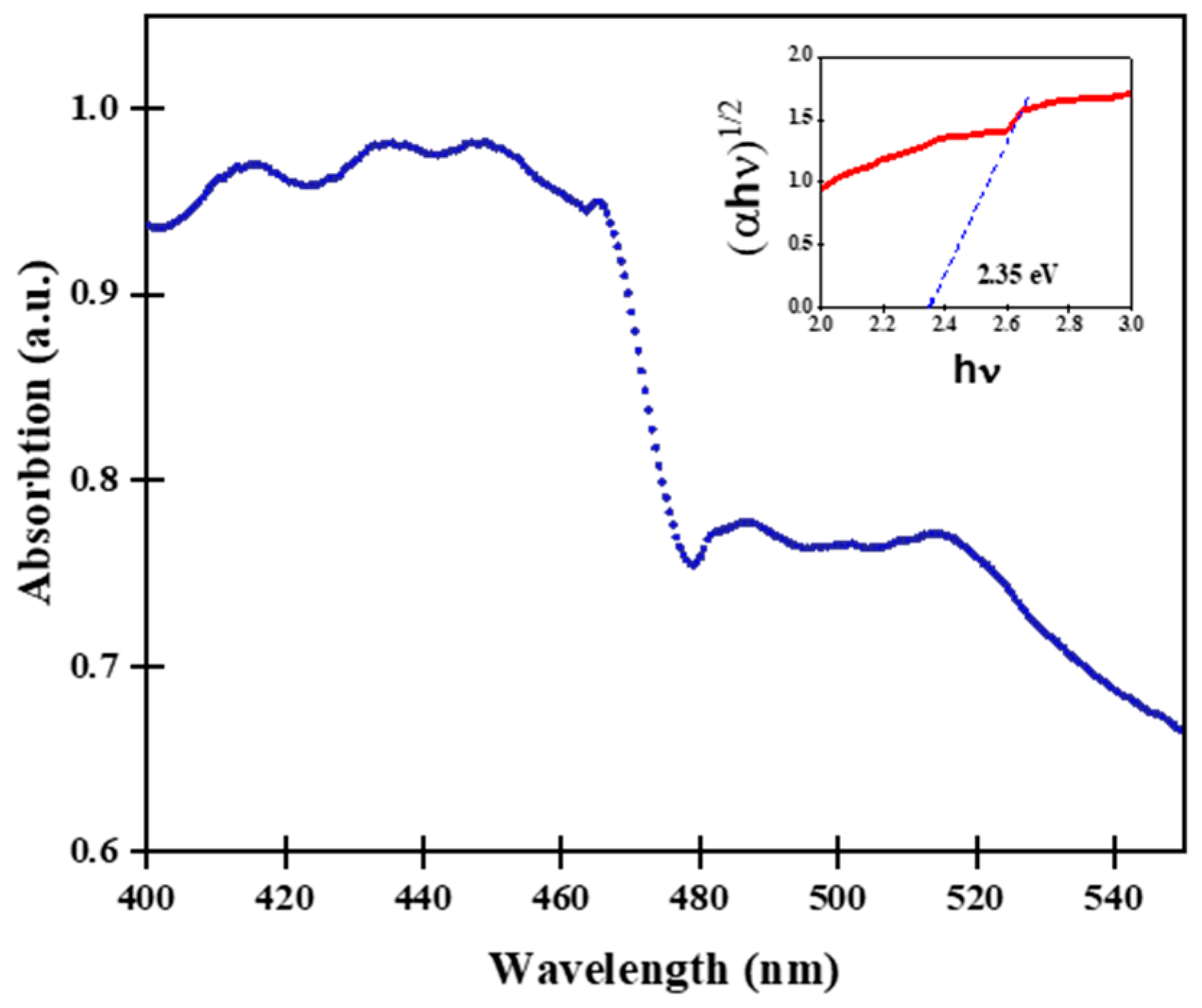
First, we looked into the optical bandgap of MABiCl by measuring optical absorption with a UV-Vis spectrometer. We obtained the absorption spectra of MABiCl, as shown in Figure 1, and corresponding Tauc [28] plot (inset). The relatively wide bandgap of ~2.35 eV is advantageous for radiation-induced current measurements by improving signal contrast upon gamma-ray exposure.
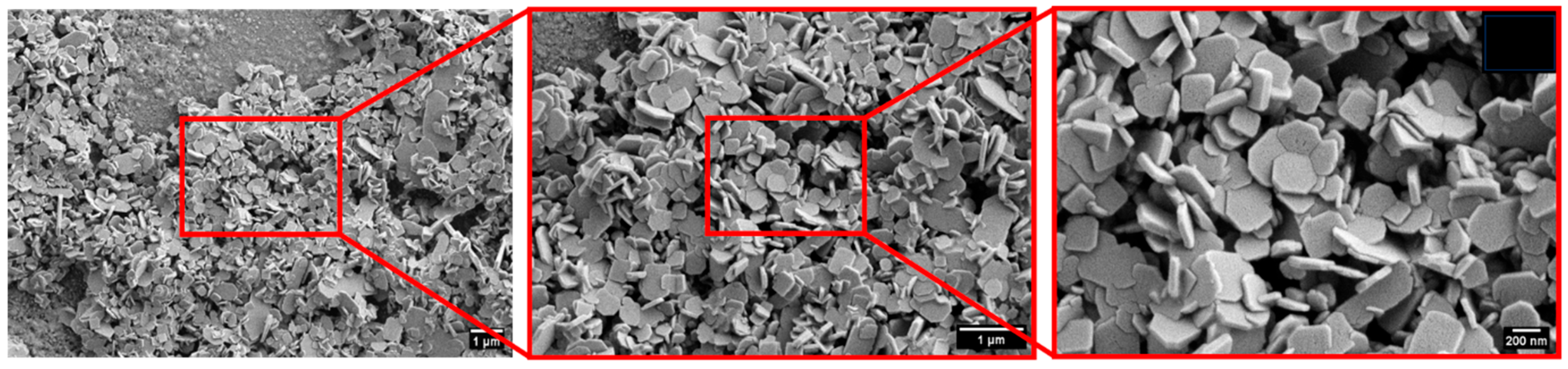
For microstructures of the perovskite sample MABiCl, we obtained SEM images with different magnifications, depicted in Figure 2. The data clearly indicate the homogenous growth of distinct flake-like hexagonal-shaped structures. The SEM images reveal relatively homogeneous, flake-like crystallites distributed across the pellet surface, suggesting uniform grain formation. Such morphological uniformity is beneficial for ensuring consistent electrical contact and reproducible current response during repeated irradiation cycles.
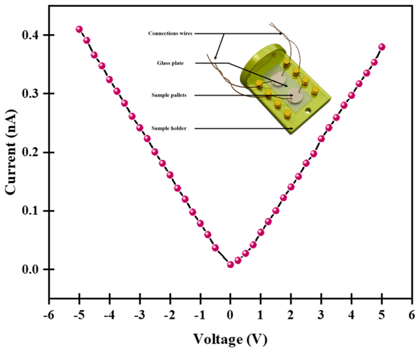
The I–V electrical characteristics of the MABiCl sample were measured on a pelletized sample at room temperature in vacuum conditions in the applied bias range of 0–5 V, as shown in Figure 3. The I–V characteristics of the MABiCl exhibit an approximately linear response within the measured bias range, indicating quasi-ohmic contact behavior between the electrodes and the sample (pellet). This linearity suggests that the measured-current changes under irradiation are not dominated by contact effects but rather reflect bulk or near-bulk charge transport processes.
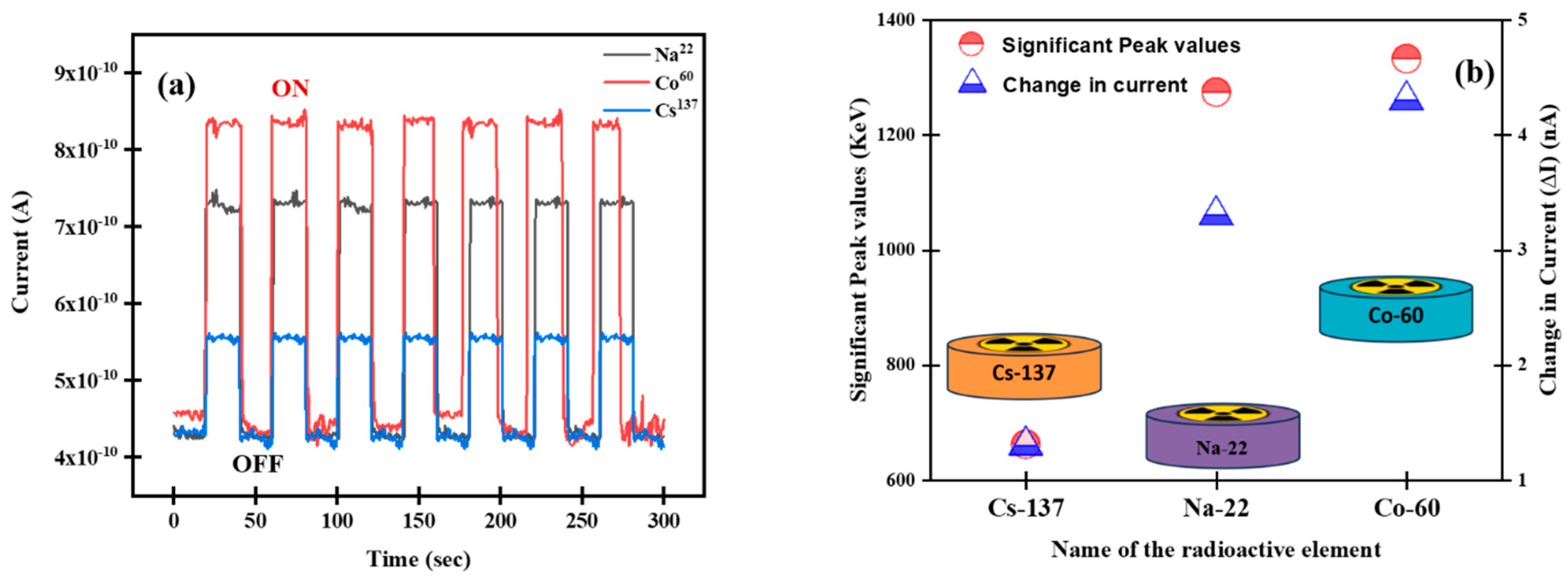
Upon exposure to gamma irradiation, the time-dependent current measurements exhibit a clear and repeatable increase in current, followed by a return toward baseline levels when the radiation source is removed, as shown in Figure 4a. This reversible behavior is consistently observed across multiple on/off cycles, indicating the stable electrical response of the perovskite under gamma irradiation. The transient nature of the current spikes suggests radiation-induced charge generation and transport; however, the detailed mechanisms responsible for the observed response require further investigations.
A comparative analysis of the current change ( Δ I ) , defined as the increase in current relative to the baseline value, is presented in Figure 4b for different gamma-ray sources. The results show a systematic variation in the magnitude of Δ I with the characteristic energy of the incident gamma radiation. While a systematic change in the measured-current response is observed for different sources, the present data do not allow for a quantitative correlation based solely on peak gamma-ray energy, as the activity of the sources and the resulting dose rate also contribute to the measured current. Within these limitations, the results indicate that the material exhibits distinguishable electrical responses under different gamma irradiation conditions. It is observed that the ΔI values corresponding to 137Cs and 60Co are relatively close to those expected based on their characteristic gamma energies, whereas for 22Na, the extracted ΔI appears to deviate from this trend. This behavior may be attributed to the decay characteristics of 22Na, which produces both a 1274.5 keV gamma photon and additional 511 keV annihilation photons that can influence the effective energy deposition in the sample. A detailed dose-rate- and activity-dependent analysis will be required to fully quantify this behavior and is planned as part of future work.

4. Conclusions

We present here a brief report on a preliminary investigation of the structural, optical, and gamma-ray-induced electrical response of Bi-based hybrid halide (MABiCl) perovskite material. Optical measurements indicate a wide bandgap suitable for radiation-induced charge generation. Electrical characterization using I–V and time-dependent I–t measurements under irradiation from different gamma sources reveals clear and reproducible current modulation correlated with gamma-ray exposure. Although the detailed physical mechanisms governing the radiation response are yet to be fully understood, the observed current spikes provide direct experimental evidence of a relationship between gamma irradiation and electrical response in the material. Future efforts will focus on integrating the material with a standard radiation counter setup and performing systematic measurements to enable quantitative analysis and a more practical detection configuration. Overall, the results establish the feasibility of Bi-based hybrid halide perovskite for gamma-ray sensing and provide a foundation for further experimental investigations.

Author Contributions

Conceptualization, P.C. and S.K.M.; methodology, P.C. and S.K.M.; software, P.C.; validation, P.C. and S.K.M.; formal analysis, P.C.; investigation, P.C. and S.K.M.; resources, S.K.M.; data curation, P.C.; writing—original draft preparation, P.C.; writing—review and editing, P.C. and S.K.M.; visualization, P.C.; supervision, S.K.M.; project administration, S.K.M.; funding acquisition, S.K.M. All authors have read and agreed to the published version of the manuscript.

Funding

This research was funded by CSIR, New Delhi, Govt. of India, grant number [03/1489/2023].

Institutional Review Board Statement

Not applicable.

Informed Consent Statement

Not applicable.

Data Availability Statement

All the data reported here can be available from the corresponding author upon reasonable request.

Conflicts of Interest

The authors declare no conflict of interest.

References

  1. Eisen, Y.; Shor, A.; Mardor, I. CdTe and CdZnTe Gamma Ray Detectors for Medical and Industrial Imaging Systems. Nucl. Instrum. Methods Phys. Res. Sect. A Accel. Spectrometers Detect. Assoc. Equip. 1999, 428, 158–170. [Google Scholar] [CrossRef] [Scilit]
  2. Hoheisel, M. Review of Medical Imaging with Emphasis on X-Ray Detectors. Nucl. Instrum. Methods Phys. Res. Sect. A Accel. Spectrometers Detect. Assoc. Equip. 2006, 563, 215–224. [Google Scholar] [CrossRef] [Scilit]
  3. Szeles, C. CdZnTe and CdTe Materials for X-Ray and Gamma Ray Radiation Detector Applications. Phys. Status Solidi B 2004, 241, 783–790. [Google Scholar] [CrossRef] [Scilit]
  4. Kalaga, D.V.; Kulkarni, A.V.; Acharya, R.; Kumar, U.; Singh, G.; Joshi, J.B. Some Industrial Applications of Gamma-Ray Tomography. J. Taiwan Inst. Chem. Eng. 2009, 40, 602–612. [Google Scholar] [CrossRef] [Scilit]
  5. Knödlseder, J. The future of gamma-ray astronomy. Comptes Rendus Phys. 2016, 17, 663–678. [Google Scholar] [CrossRef] [Scilit]
  6. McConnell, M.L.; Bloser, P.F.; Legere, J.; Ryan, J.M. Applications for New Scintillator Technologies in Gamma Ray Astronomy. J. Phys. Conf. Ser. 2016, 763, 012008. [Google Scholar] [CrossRef] [Scilit]
  7. Milbrath, B.D.; Peurrung, A.J.; Bliss, M.; Weber, W.J. Radiation Detector Materials: An Overview. J. Mater. Res. 2008, 23, 2561–2581. [Google Scholar] [CrossRef] [Scilit]
  8. Sordo, S.D.; Abbene, L.; Caroli, E.; Mancini, A.M.; Zappettini, A.; Ubertini, P. Progress in the Development of CdTe and CdZnTe Semiconductor Radiation Detectors for Astrophysical and Medical Applications. Sensors 2009, 9, 3491–3526. [Google Scholar] [CrossRef] [Scilit]
  9. Kojima, A.; Teshima, K.; Shirai, Y.; Miyasaka, T. Organometal Halide Perovskites as Visible-Light Sensitizers for Photovoltaic Cells. J. Am. Chem. Soc. 2009, 131, 6050–6051. [Google Scholar] [CrossRef] [Scilit]
  10. Dou, L.; Yang, Y.M.; You, J.; Hong, Z.; Chang, W.-H.; Li, G.; Yang, Y. Solution-Processed Hybrid Perovskite Photodetectors with High Detectivity. Nat. Commun. 2014, 5, 5404. [Google Scholar] [CrossRef] [Scilit]
  11. Shrestha, S.; Fischer, R.; Matt, G.J.; Feldner, P.; Michel, T.; Osvet, A.; Levchuk, I.; Merle, B.; Golkar, S.; Chen, H.; et al. High-Performance Direct Conversion X-Ray Detectors Based on Sintered Hybrid Lead Triiodide Perovskite Wafers. Nat. Photonics 2017, 11, 436–440. [Google Scholar] [CrossRef] [Scilit]
  12. Li, L.; Liu, X.; Zhang, H.; Zhang, B.; Jie, W.; Sellin, P.J.; Hu, C.; Zeng, G.; Xu, Y. Enhanced X-Ray Sensitivity of MAPbBr3 Detector by Tailoring the Interface-States Density. ACS Appl. Mater. Interfaces 2019, 11, 7522–7528. [Google Scholar] [CrossRef] [Scilit]
  13. Tsai, H.; Liu, F.; Shrestha, S.; Fernando, K.; Tretiak, S.; Scott, B.; Vo, D.T.; Strzalka, J.; Nie, W. A Sensitive and Robust Thin-Film x-Ray Detector Using 2D Layered Perovskite Diodes. Sci. Adv. 2020, 6, eaay0815. [Google Scholar] [CrossRef] [Scilit] [PubMed]
  14. Wei, W.; Zhang, Y.; Xu, Q.; Wei, H.; Fang, Y.; Wang, Q.; Deng, Y.; Li, T.; Gruverman, A.; Cao, L.; et al. Monolithic Integration of Hybrid Perovskite Single Crystals with Heterogenous Substrate for Highly Sensitive X-Ray Imaging. Nat. Photonics 2017, 11, 315–321. [Google Scholar] [CrossRef] [Scilit]
  15. Kim, Y.C.; Kim, K.H.; Son, D.-Y.; Jeong, D.-N.; Seo, J.-Y.; Choi, Y.S.; Han, I.T.; Lee, S.Y.; Park, N.-G. Printable Organometallic Perovskite Enables Large-Area, Low-Dose X-Ray Imaging. Nature 2017, 550, 87–91. [Google Scholar] [CrossRef] [Scilit]
  16. Maity, A.; Das, C.; Raychaudhuri, A.K.; Saha, A.; Ghosh, B. Highly Radiation Resistant Room Temperature Organic Perovskite Halide (FAPbI3) Crystal for Direct Detection of Gamma-Ray Photons down to Nano Curie Activity. J. Phys. D Appl. Phys. 2021, 54, 455104. [Google Scholar] [CrossRef] [Scilit]
  17. He, Y.; Stoumpos, C.C.; Hadar, I.; Luo, Z.; McCall, K.M.; Liu, Z.; Chung, D.Y.; Wessels, B.W.; Kanatzidis, M.G. Demonstration of Energy-Resolved γ-Ray Detection at Room Temperature by the CsPbCl3 Perovskite Semiconductor. J. Am. Chem. Soc. 2021, 143, 2068–2077. [Google Scholar] [CrossRef] [Scilit] [PubMed]
  18. He, Y.; Petryk, M.; Liu, Z.; Chica, D.G.; Hadar, I.; Leak, C.; Ke, W.; Spanopoulos, I.; Lin, W.; Chung, D.Y.; et al. CsPbBr3 Perovskite Detectors with 1.4% Energy Resolution for High-Energy γ-Rays. Nat. Photonics 2021, 15, 36–42. [Google Scholar] [CrossRef] [Scilit]
  19. Yakunin, S.; Dirin, D.N.; Shynkarenko, Y.; Morad, V.; Cherniukh, I.; Nazarenko, O.; Kreil, D.; Nauser, T.; Kovalenko, M.V. Detection of Gamma Photons Using Solution-Grown Single Crystals of Hybrid Lead Halide Perovskites. Nat. Photonics 2016, 10, 585–589. [Google Scholar] [CrossRef] [Scilit]
  20. He, Y.; Matei, L.; Jung, H.J.; McCall, K.M.; Chen, M.; Stoumpos, C.C.; Liu, Z.; Peters, J.A.; Chung, D.Y.; Wessels, B.W.; et al. High Spectral Resolution of Gamma-Rays at Room Temperature by Perovskite CsPbBr3 Single Crystals. Nat. Commun. 2018, 9, 1609. [Google Scholar] [CrossRef] [Scilit]
  21. He, Y.; Ke, W.; Alexander, G.C.B.; McCall, K.M.; Chica, D.G.; Liu, Z.; Hadar, I.; Stoumpos, C.C.; Wessels, B.W.; Kanatzidis, M.G. Resolving the Energy of γ-Ray Photons with MAPbI3 Single Crystals. ACS Photonics 2018, 5, 4132–4138. [Google Scholar] [CrossRef] [Scilit]
  22. Wei, H.; DeSantis, D.; Wei, W.; Deng, Y.; Guo, D.; Savenije, T.J.; Cao, L.; Huang, J. Dopant Compensation in Alloyed CH3NH3PbBr3−xClx Perovskite Single Crystals for Gamma-Ray Spectroscopy. Nat. Mater. 2017, 16, 826–833. [Google Scholar] [CrossRef] [Scilit]
  23. Li, J.; Cao, H.-L.; Jiao, W.-B.; Wang, Q.; Wei, M.; Cantone, I.; Lü, J.; Abate, A. Biological Impact of Lead from Halide Perovskites Reveals the Risk of Introducing a Safe Threshold. Nat. Commun. 2020, 11, 310. [Google Scholar] [CrossRef] [Scilit] [PubMed]
  24. Chandra, P.; Saha, S.; Mandal, S.K. A Dielectric Study of Br-Doped Lead-Free Methylammonium Bismuth Chloride (CH3NH3)3Bi2BrxCl9−x. Appl. Phys. A 2022, 128, 541. [Google Scholar] [CrossRef] [Scilit]
  25. Chandra, P.; Mandal, S.K. Observation of Negative Photoconductivity in (CH3NH3)3Bi2(BrxCl1–x)9: Correlating Ion Migration, Stability, and Efficiency in Mixed Halide Perovskite Solar Cell. J. Phys. Chem. C 2023, 127, 23109–23121. [Google Scholar] [CrossRef] [Scilit]
  26. Ahmed, I.; Prakash, K.; Mobin, S.M. Lead-Free Perovskites for Solar Cell Applications: Recent Progress, Ongoing Challenges, and Strategic Approaches. Chem. Commun. 2025, 61, 6691–6721. [Google Scholar] [CrossRef] [Scilit] [PubMed]
  27. Chandra, P.; Mandal, S.K. Morphology Controlled (CH3NH3)3Bi2Cl9 Thin Film for Lead Free Perovskite Solar Cell. Phys. B Condens. Matter 2021, 625, 413536. [Google Scholar] [CrossRef] [Scilit]
  28. Tauc, J. Optical Properties and Electronic Structure of Amorphous Ge and Si. Mater. Res. Bull. 1968, 3, 37–46. [Google Scholar] [CrossRef] [Scilit]
  29. X-Ray and Gamma Ray Decay Data. Available online: https://www-nds.iaea.org/xgamma_standards/ (accessed on 24 December 2025).
Figure 1. UV–Vis absorption spectrum of the MABiCl material (in blue) along with the corresponding Tauc plot (inset in red), indicating a wide optical bandgap.
Materproc 26 00013 g001
Figure 2. SEM images of the MABiCl sample recorded at three different magnifications, showing the surface morphology of the pelletized material.
Materproc 26 00013 g002
Figure 3. Current-voltage (I–V) characteristics of the pelletized MABiCl sample measured at room temperature. The approximately linear and symmetric I–V response within the applied bias range indicates stable electrical behavior of the sample and suggests quasi-ohmic contact between the electrodes and the perovskite pellet.
Materproc 26 00013 g003
Figure 4. (a) I-t plot of the MABiCl with three different gamma sources, 60Co (1332 keV), 137Cs (662 keV), and 22Na (1274 keV) [29], respectively. The plots show clear and reproducible current modulation corresponding to radiation on/off cycles, indicating a measurable electrical response of the material upon gamma-ray exposure. (b) Comparative plot showing the change in current ( Δ I ) with incident gamma energy.
Materproc 26 00013 g004
Disclaimer/Publisher’s Note: The statements, opinions and data contained in all publications are solely those of the individual author(s) and contributor(s) and not of MDPI and/or the editor(s). MDPI and/or the editor(s) disclaim responsibility for any injury to people or property resulting from any ideas, methods, instructions or products referred to in the content.