Proceeding Paper

Fabrication and Characterization of Tungsten-Modified TiO2 as a Photo-Anode in a Dye-Sensitized Solar Cell †

1
Graduate Institute of Aeronautics, Department of Information and Communication Engineering, Chaoyang University of Technology, Taichung 413310, Taiwan
2
Department of Electrical Engineering, Tunghai University, Taichung 413310, Taiwan
3
Graduate Institute of Aeronautics, Chaoyang University of Technology, Taichung 413310, Taiwan
4
Department of Electronic Engineering, Cheng Shiu University, Kaohsiung 83347, Taiwan
5
Department of Electronic Engineering, National Changhua University of Education, Changhua 50074, Taiwan
6
Department of Electronic Engineering, Feng Chia University, Taichung 407102, Taiwan
*
Author to whom correspondence should be addressed.
Presented at the 2024 IEEE 6th Eurasia Conference on IoT, Communication and Engineering, Yunlin, Taiwan, 15–17 November 2024.
Eng. Proc. 2025, 92(1), 76; https://doi.org/10.3390/engproc2025092076
Published: 21 May 2025
(This article belongs to the Proceedings of 2024 IEEE 6th Eurasia Conference on IoT, Communication and Engineering)

Abstract

:
The tungsten (W)-modified TiO2 films were fabricated on the fluorine-doped TiO2 substrates using the sol–gel process. The influences of W dopant on the photovoltaic properties of the tungsten-modified TiO2 DSSC were analyzed, too. The crystallization and dye absorption of tungsten-modified TiO2 thin films increased more than those of the undoped TiO2 thin films. Furthermore, the optimal performances of the Voc, Jsc, fill factor, and efficiency of the DSSC with tungsten-modified TiO2 thin films were 0.68 V, 16.28 mA/cm2, 65.5%, and 7.03%, respectively. The enhancement was mainly due to the improved crystallinity and increased dye adsorption of the tungsten-modified TiO2 thin films, which contributed to improving the efficiency of the dye-sensitized solar cell.

1. Introduction

Due to its superior electronic conductivity, high-specific-surface-area nanostructure, fast ion migration characteristics, and stable chemical properties, TiO2 has become one of the main materials used to create dye-sensitized solar cells (DSSCs) [1,2,3,4,5,6,7,8,9,10]. By doping different elements into the TiO2 lattice, Ti⁴⁺ ions are replaced, thereby changing the energy band structure of the material. Doping different elements can adjust the energy gap to a range more conducive to light absorption, further improving its optical and electronic properties [11,12,13,14,15,16,17]. The introduction of doping elements allows for lattice distortion, thereby increasing the concentration of lattice defects. These defects serve as charge-trapping centers, improving the separation efficiency of electron–hole pairs and increasing the open circuit voltage of the device. They also improve the photoelectric conversion efficiency of DSSC. Doped TiO2 films usually exhibit larger grains and a specific surface area. These characteristics significantly enhance the light scattering effect of the photoelectrode layer, thereby improving the multiple reflection mechanism of light and extending the optical path of photons in the battery [18,19,20]. As the grain size increases, the light path within the cell is lengthened, allowing more dye molecules to absorb photons and excite more electrons. In addition, the increase in specific surface area increases the number of attached dye molecules and enhances the generation of photogenerated electrons. This improves the transmission and separation efficiency of photogenerated carriers. The photoelectric conversion efficiency of DSSC is significantly improved.
Many researchers have fabricated TiO2 thin films using various methods, including spray pyrolysis [21,22] sputtering, microwave-assisted method [23], sol–gel [24,25], the chemical solution method, and metal–organic decomposition [26,27]. Among them, the sol–gel technique provides the most flexible and precise control of stoichiometry, such that precise stoichiometric ratios and uniform composition distribution can be obtained for the TiO2 films. The chemical composition of the solution can be adjusted to permeate the sol to achieve specific membrane properties and structures. This precise stoichiometric control fine-tunes the structure, composition, and thickness of the film to meet the needs of different applications. Sol–gel technology is also used to fabricate TiO2 films with nanostructures and porous structures, which is significant for special applications, such as DCCSs.
We investigated the effect of tungsten (W) doping concentration on the structural and optical properties of TiO2 thin films, along with its performance in DSSCs. Tungsten was chosen as the dopant due to its ion radius being close to that of Ti, allowing for an effective substitution of Ti in the TiO2 lattice, thereby forming a stable doped structure. Additionally, sol–gel technology was selected as the preparation method for tungsten-doped TiO2 thin films. The technique is relatively underexplored but offers potential for material optimization. In this study, the structural, optical, surface, and optoelectronic properties of the tungsten-doped TiO2 thin film were measured and analyzed. The crystal structure was examined through X-ray diffraction (XRD) to determine whether the crystal phase of TiO2 was altered by W doping. Optical properties were assessed to evaluate the impact on light absorption. The photoelectric conversion efficiency of DSSCs at different doping concentrations was measured using photocurrent–voltage (I-V) curves.

2. Experiment

In the preparation, titanium diisopropoxide bis(2,4-pentanedione) (TIAA) and tungsten isopropoxide were selected as precursors to synthesize tungsten-doped TiO2 films. First, TIAA and tungsten isopropoxide were dissolved in a specific volume of ethanol, and the solution was continuously stirred at room temperature for 2 h to ensure uniform dispersion of the precursors. The molar concentration of W relative to TiO2 was adjusted to 7% to obtain the best doping effect. After the stirring was completed, the solution gradually entered the gelation process by controlling the evaporation rate of the solvent, and the formed gel was cooled and aged at 80 °C for 2 h to increase the uniformity and stability of the composition. Finally, a gold stock solution with a concentration of approximately 1 M was obtained as a starting material for subsequent preparations. To transform the gel into a stable tungsten-doped TiO2 structure, the gel was sintered at a high temperature. In the sintering process, the temperature was raised to 500–700 °C and maintained for 2 h to completely remove any residual solvents and organic components. This step rearranged the TiO2 lattice and made the tungsten doping evenly distributed. In the crystal lattice, the target crystal structure was formed.
To prepare DSSC, the sintered tungsten-doped TiO2 film was soaked in an N3 dye ethanol solution with a concentration of 3 × 10⁻⁴ M and left at room temperature for 24 h to allow the dye to be fully adsorbed on the TiO2 surface to form a stable dye-sensitized layer. Afterward, the dye-sensitized photoelectrode was rinsed with absolute ethanol to remove unbound dye molecules and dried in a nitrogen environment or at a low temperature to protect the dye layer and prevent desorption or degradation. In the preparation process of the counter electrode, a platinum-coated FTO substrate was used as the counter electrode. A chloroplatinic acid solution was dropped onto the surface of the substrate and then annealed at 400 °C for 30 min to enhance the conductivity and catalytic activity of the substrate for charge exchange needs. For the preparation and injection of the electrolyte solution, a solution containing iodide ions/triiodide ions (I/I3) was selected as the electrolyte, and it was injected between the TiO2 electrode and the counter electrode. After assembly, UV curing glue was used to seal the entire cell to ensure that the electrolyte would not leak and prevent the degradation of photovoltaic performance. Finally, the photoelectric conversion performance of the DSSC was tested by using a xenon lamp with a monochromator to determine the photoelectric conversion efficiency of the tungsten-doped TiO2 film at different wavelengths. This multi-step preparation process was conducted to ensure the uniformity, stability, and high photoelectric conversion performance of the tungsten-doped TiO2 film in DSSC, providing theoretical and process support for this material in photovoltaic applications.

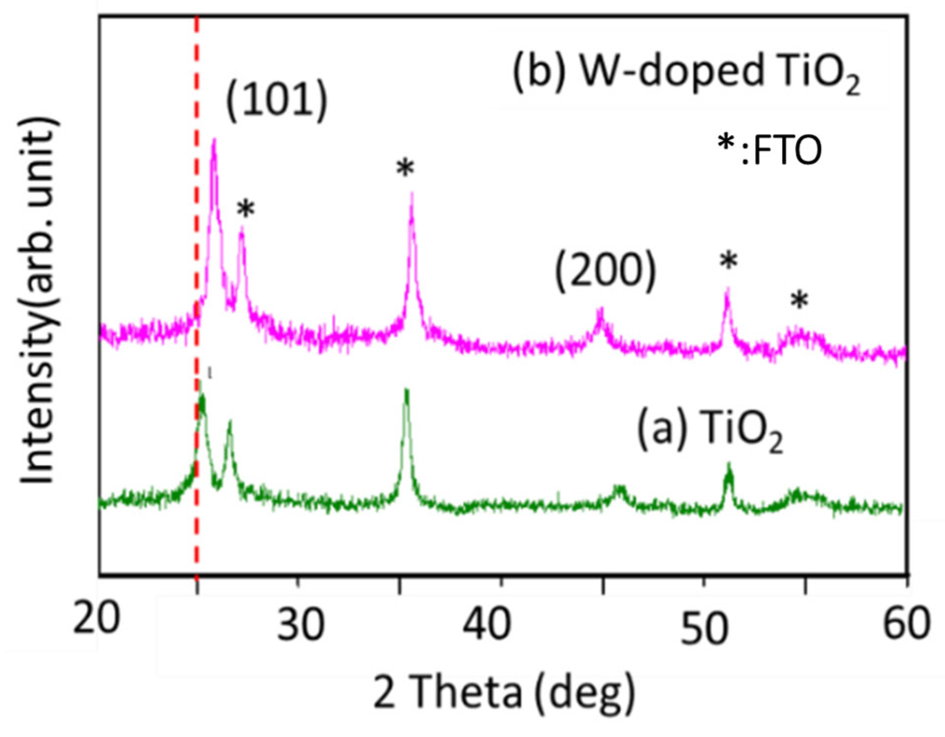
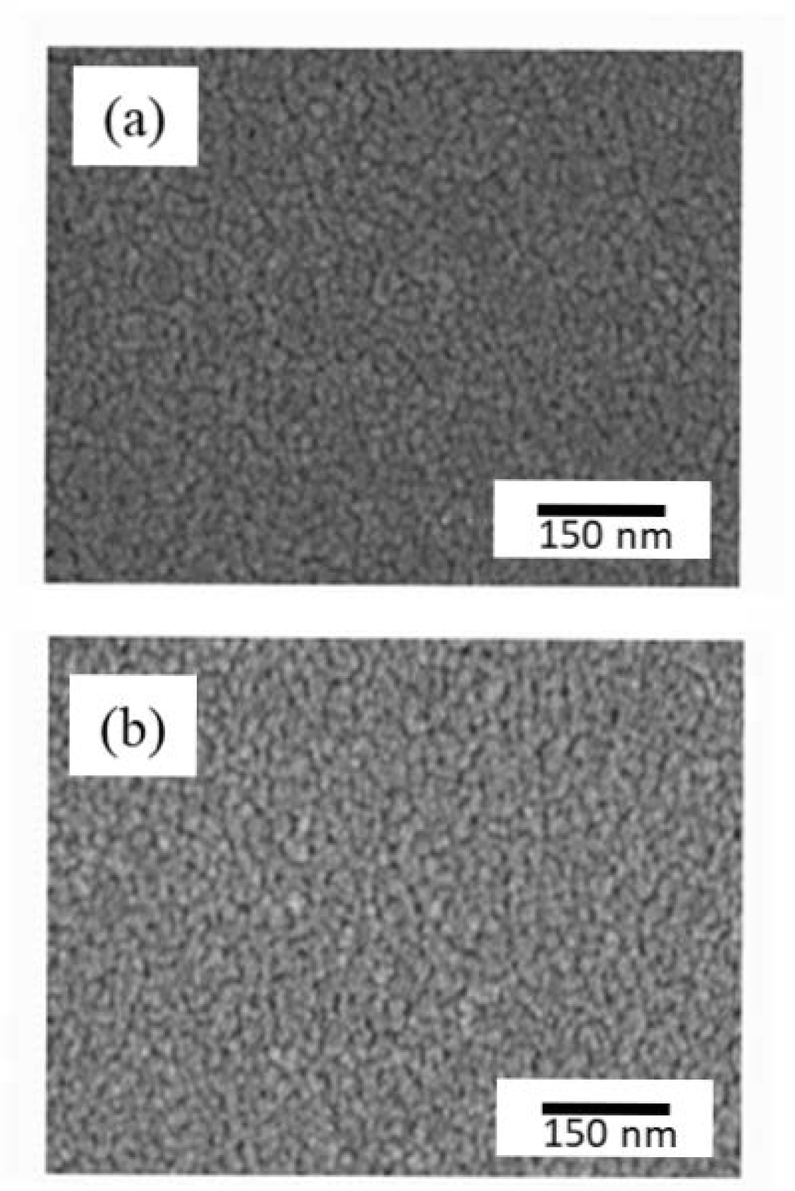
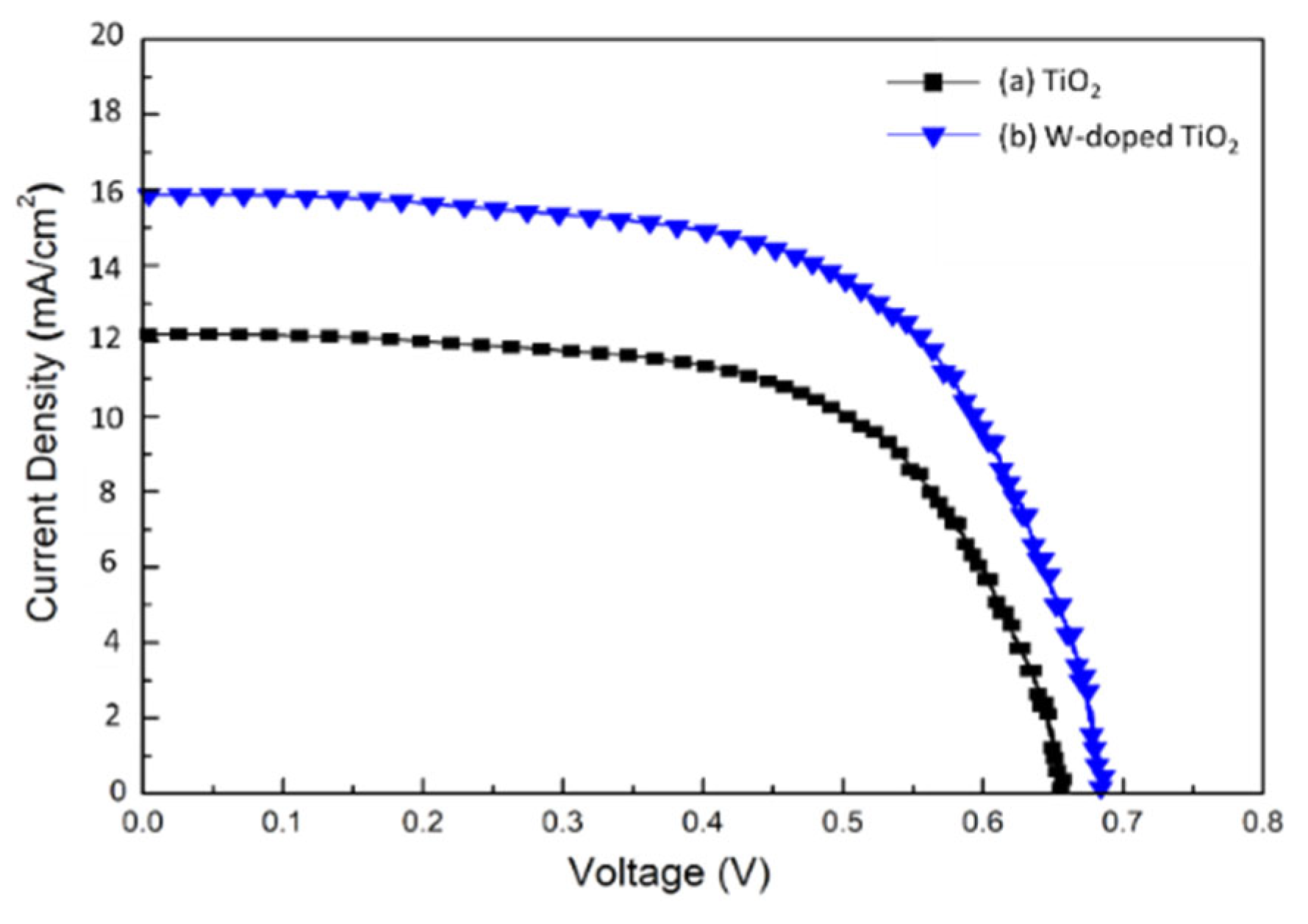
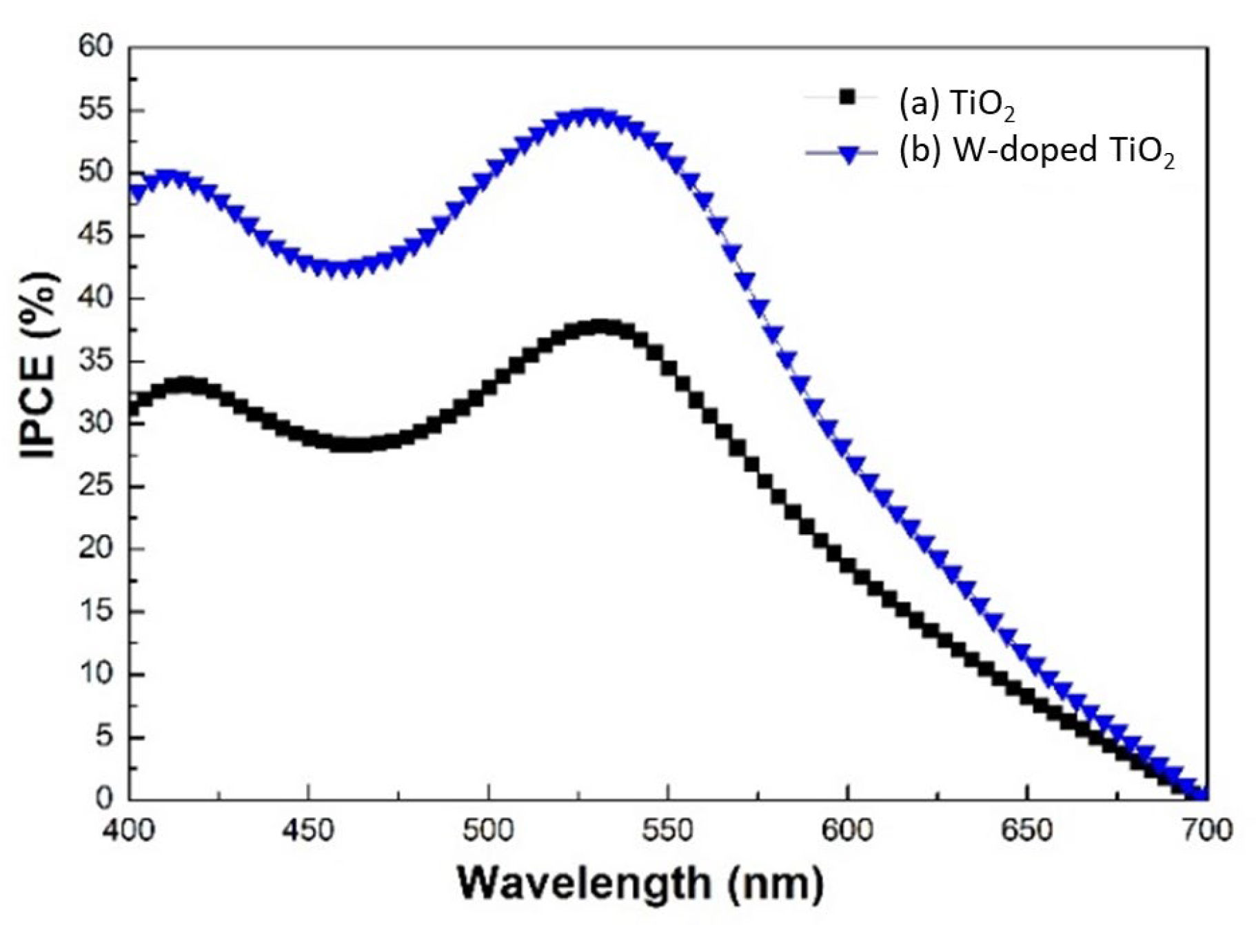
3. Result and Discussion

All diffraction peaks corresponding to the TiO2 anatase structure with a tetragonal central structure and (101) preferred orientation are shown in Figure 1. Compared with the pure TiO2 film, the diffraction peak intensity of the tungsten (W)-doped TiO2 film on the (101) plane was significantly enhanced, which indicated that W doping enhanced the order of the crystal. Furthermore, the (101) peak position of the W-doped film shifted toward higher 2θ values, indicating a slight shrinkage of the unit cell due to the partial replacement of Ti ions by W ions or the occupation of interstitial positions in the TiO2 crystal. Since the ionic radii of W (0.60 Å) and Ti (0.605 Å) are close, during the doping process, W ions replace Ti ions in the crystal lattice, thus achieving a stable doping structure [28,29].
XRD was applied to determine the crystallite size (D) of the film, using the main diffraction peak position of the (101) plane (2θ = 25.1°), and the Scherrer Equation (1) was used to calculate the average size of the crystals [30].
D = 0.89 λ β c o s θ
where D represents the crystallite size, λ is the wavelength of the X-ray, β is the full width at half maximum of the diffraction peak, and θ is the Bragg angle.
The crystallite size of the undoped TiO2 film was 22.5 nm, while the crystallite size of the W-doped TiO2 film was 25.6 nm. This shows that W doping increased the TiO2 crystal size due to the change in crystal growth rate and the enhancement of the stability of the lattice structure caused by the doping element. In addition, the increased crystal size promoted the optical and electronic properties of TiO2 films. A larger crystallite size reduces the number of grain boundaries, thereby reducing the scattering and recombination rate of electrons at grain boundaries, which is important for DSSC. As they exhibit fewer electron recombination phenomena, W-doped TiO2 films enable higher charge transfer efficiency, thereby improving the photoelectric conversion efficiency of DSSC. Therefore, this increase in crystallite size is closely related to the improvement of the photoelectric properties of TiO2 films, and thus has more potential in photovoltaic applications.
Figure 2 shows the evolution of the surface microstructure of TiO2 and tungsten-modified TiO2 films. With W doping, the grain size and porosity increased significantly. After W ions are doped into the TiO2 lattice, due to the different ionic radii of W ions and Ti ions, as well as the difference in bond energy between W–O and Ti–O, the nucleation and growth kinetics of TiO2 are affected. Larger W ions replace Ti ions in the crystal lattice, which causes crystal distortion and enhances the grain boundary stress inside the film. This lattice distortion and grain boundary stress affect the growth path of the crystal grains and change the pore distribution of the film, causing more voids to appear in the grains during the growth process, and thus increasing the porosity of the film. In addition, due to the increase in porosity, the specific surface area of the film increases, which enhances the adsorption of dyes in subsequent DSSC, further improving its light absorption capacity and photoelectric conversion efficiency. It also effectively enhances its potential in photovoltaic applications.
Brunauer–Emmett–Teller (BET) analysis of thin films is conducted to measure the surface area of a material, measuring the amount of surface-adsorbed dye. Based on the results, the optimal film preparation conditions can be found to obtain the maximum specific surface area and optimal dye adsorption performance. BET analysis can be used to improve the optoelectronic performance of DSSC. Table 1 shows the increase in W content, the surface area of the film, and the increase in the amount of adsorbed dye. The surface area increased from 42 to 56 m2/g, and the amount of adsorbed dye increased from 1.98 × 10⁻⁸ to 2.75 × 10⁻⁸ mol/cm2. The results indicate that the tungsten-doped TiO2 thin films exhibit the highest adsorption capacity. This was attributed to the notable increase in crystallite size and porosity of the tungsten-modified TiO2 thin films [31]. Improvements in grain size and pore structure increase the collection and transmission of photoelectrons and improve the light absorption and efficiency of DSSCs.
The I-V curve of DSSC of the TiO2 and tungsten-modified TiO2 thin film is shown in Figure 3. The I-V curve illustrates the performance characteristics of a solar cell at various voltage and current levels. Where the short-circuit photocurrent density (Jsc) is the current density generated by the DSSC under short-circuit conditions, and Voc is the voltage of the DSSC under open-circuit conditions. Additionally, the fill factor (FF) is defined as the ratio of the rectangular area under the I-V curve to the maximum achievable power area. Conversion efficiency (η) represents the efficiency of DSSC, as follows.
η = J s c × V o c × F F P i n
When Pin was set at 1000 W/m2, Jsc increased from 12.2 to 16.28 mA/cm2. This enhancement is attributed to the increased specific surface area of the tungsten-doped TiO₂ thin film, resulting from the notable rise in crystallite size and porosity. This expanded surface area facilitates greater dye molecule adsorption, thereby improving the dye-loading capacity. In addition, the tungsten-modified TiO2 thin film has a TiO2 anatase structure with a higher (101) orientation, which is beneficial to the movement of electrons within the material. The efficiency of the tungsten-doped TiO₂ thin-film DSSCs reached 7.03%, which is better than the conversion efficiency (2.47%) of the DSSCs produced using the solid-phase method in previous studies [28]. The photovoltaic performance parameters are summarized in Table 2.
Figure 4 shows the incident photon-to-electron conversion efficiency (IPCE) of DSSCs. The IPCE is defined as follows.
I P C E = 1240 × J s c ( m A / c m 2 ) λ n m × I i n c ( m W / m 2 )
where Jsc represents the photocurrent density in the short-circuit state, while Iinc is the intensity of incident monochromatic light at a specific excitation wavelength λ.
IPCE represents the proportion of current electrons generated by each incident photon and is an important parameter for evaluating photoelectric conversion performance. IPCE is a key metric, since it directly reflects the combined efficiency of light absorption, charge separation, and electron transport. Compared with undoped TiO2 thin-film DSSCs, the IPCE of tungsten-modified TiO2 thin-film DSSCs is significantly improved. This indicates that W doping plays an important role in enhancing solar energy conversion efficiency. The introduction of W expands the light absorption range of TiO2, especially the light-capturing ability in the visible-light range. The separation and efficient transport of photogenerated electrons reduces the chance of charge recombination. In addition, since W doping increases the microporous structure and specific surface area of the TiO2 film, it facilitates the adsorption of more dye molecules and enhances the photon absorption efficiency. The IPCE improvement of tungsten-modified TiO2 thin-film DSSC at different wavelengths also reflects its stability and response under various spectral conditions, proving the effectiveness of tungsten doping in improving photoelectrode performance. This improvement is attributed to a better photoelectric conversion path as well as optimized electron transport kinetics, allowing the cell to convert solar energy into electricity with higher efficiency, further demonstrating the potential of tungsten-doped TiO2 films in photovoltaic applications.

4. Conclusions

The influence of tungsten doping on the properties of TiO2 thin film-based DSSCs was investigated in this study. The tungsten-doped TiO2 thin film exhibits an optimal dye adsorption capacity of 2.75 × 10⁻⁸ mol/cm2. In addition, the DSSC of tungsten-modified TiO2 thin film also has higher Jsc, Voc, FF, and η values, which are 0.68 V, 16.28 mA/cm2, 63.5%, and 7.03%, respectively. This is attributed to the tungsten-modified TiO2 thin film having the best (101)-oriented TiO2 anatase crystal growth and the highest dye adsorption capacity. It is beneficial to the movement of electrons in the material and improves the electron transmission performance. The W-modified TiO2 thin film has a larger specific surface area due to the significant increase in crystal size and porosity.

Author Contributions

Conceptualization, M.-C.K. and C.-H.C.; methodology, M.-C.K. and C.-H.C.; formal analysis, M.-C.K., T.-K.K. and C.-H.C.; investigation, J.-H.W.; resources, K.-H.C.; data curation, M.-C.K.; writing—original draft preparation, K.-H.C. and C.-H.C.; writing—review and editing, T.-K.K.; visualization, M.-C.K. and D.-Y.L.; project administration, M.-C.K. and D.-Y.L.; funding acquisition, C.-H.C. All authors have read and agreed to the published version of the manuscript.

Funding

This research was funded by the National Science Council of the Republic of China under grant number NSTC 113-2637-E-324-001.

Institutional Review Board Statement

Not applicable.

Informed Consent Statement

Not applicable.

Data Availability Statement

The data presented in this study are available on request from the corresponding author due to confidentiality agreement.

Conflicts of Interest

The authors declare no conflict of interest.

References

  1. Agrawal, A.; Siddiqui, S.A.; Soni, A.; Khandelwal, K.; Sharma, G.D. Performance analysis of TiO2 based dye sensitized solar cell prepared by screen printing and doctor blade deposition techniques. Sol. Energy 2021, 226, 9–19. [Google Scholar] [CrossRef]
  2. Abdullaev, S.S.; Breesam, Y.F.; AlZubaidi, A.A.H.; Tripathi, A.K.; Kareem, A.K.; Kuznetsov, S.V.; Alawsi, T.; Zabibah, R.S. ZnO@ZnCo2O4 core-shell: A novel high electrocatalytic nanostructure to replace platinum as the counter electrode in dye-sensitized solar cells. Mater. Sci. Semicond. Process. 2023, 165, 107709. [Google Scholar] [CrossRef]
  3. Patil, S.S.; Mane, R.M.; Khot, K.V.; Mali, S.S.; Hong, C.K.; Bhosale, P.N. Surfactant assisted approach to development of efficient WO3 photoanode for natural dye sensitized solar cell. Sol. Energy 2021, 220, 371–383. [Google Scholar] [CrossRef]
  4. Abrari, M.; Ghanaatshoar, M.; Davarani, S.S.H.; Moazami, H.R.; Kazeminezhad, I. Synthesis of SnO2 nanoparticles by electro oxidation of tin in quaternary ammonium salt for application in dye-sensitized solar cells. Appl. Phys. A 2017, 123, 326–329. [Google Scholar] [CrossRef]
  5. Prabakaran, S.; Nisha, K.D.; Harish, S.; Archana, J.; Navaneethan, M.; Ponnusamy, S.; Muthamizhchelvan, C.; Ikeda, H.; Hayakawa, Y. Synergistic effect and enhanced electrical properties of TiO2/SnO2/ZnO nanostructures as electron extraction layer for solar cell application. Appl. Surf. Sci. 2019, 498, 143702. [Google Scholar] [CrossRef]
  6. Vibavakumar, S.; Nish, K.D.; Manikandan, V.S.; Archana, J.; Navaneethan, M.; Harish, S. Enhanced photo conversion efficiency of Nb2O5/TiO2 bilayer photoanode for Dye-Sensitized Solar Cells. Optical Mater. 2023, 140, 113828–113835. [Google Scholar] [CrossRef]
  7. Han, Q.; Wu, C.; Jiao, H.; Xu, R.; Wang, Y.; Xie, J.; Guo, Q.; Tang, J. Rational design of high-concentration Ti3+ in porous carbon-doped TiO2 nanosheets for efficient photocatalytic ammonia synthesis. Adv. Mater. 2021, 33, 2008180. [Google Scholar] [CrossRef]
  8. Guo, Q.; Wu, J.; Yang, Y.; Liu, X.; Sun, W.; Wei, Y.; Lan, Z.; Lin, J.; Huang, M.; Chen, H.; et al. Low-temperature processed rare-earth doped brookite TiO2 scaffold for UV stable, hysteresis-free and high-performance perovskite solar cells. Nano Energy 2020, 77, 105183. [Google Scholar] [CrossRef]
  9. Liu, G.; Huang, M.; Zhang, Z.; Xi, B.; Li, H.; Xiong, S. Robust S-doped TiO2@N,S-codoped carbon nanotube arrays as free-binder anodes for efficient sodium storage. J. Energy Chem. 2021, 53, 175–184. [Google Scholar] [CrossRef]
  10. Liao, Y.-H.; Chang, Y.-H.; Lin, T.-H.; Chan, S.-H.; Lee, K.-M.; Hsu, K.-H.; Hsu, J.-F.; Wu, M.-C. Boosting the power conversion efficiency of perovskite solar cells based on Sn doped TiO2 electron extraction layer via modification the TiO2 phase junction. Sol. Energy 2020, 205, 390–398. [Google Scholar] [CrossRef]
  11. Katta, V.S.; Chappidi, V.R.; Raavi, S.S.K. Samarium-doped TiO2 photoanodes for the molecular devices for solar energy conversion. In Proceedings of the SPIE/COS Photonics Asia, Nantong, China, 10–20 October 2021. [Google Scholar] [CrossRef]
  12. Katta, V.S.; Velpandian, M.; Chappidi, V.R.; Ahmed, M.S.; Kumar, A.; Asthana, S.; Meduri, P.; Raavi, S.S.K. Er3+ doped titania photoanode for enhanced performance of photo-electrochemical water splitting devices. Mater. Lett. 2021, 302, 130297. [Google Scholar] [CrossRef]
  13. Tang, X.; Xue, Q.; Qi, X.; Cheng, C.; Yang, M.; Yang, T.; Chen, F.; Qiu, F.; Quan, X. DFT and experimental study on visible-light driven photocatalysis of rare-earth-doped TiO2. Vacuum 2022, 200, 110972. [Google Scholar] [CrossRef]
  14. Kumaravel, V.; Rhatigan, S.; Mathew, S.; Bartlett, J.; Nolan, M.; Hinder, S.J.; Sharma, P.K.; Singh, A.; Byrne, J.A.; Harrison, J.; et al. Indium-doped TiO2 photocatalysts with high-temperature anatase stability. J. Phys. Chem. C 2019, 123, 21083–21096. [Google Scholar] [CrossRef]
  15. Kong, X.; Peng, Z.; Jiang, R.; Jia, P.; Feng, J.; Yang, P.; Chi, Q.; Ye, W.; Xu, F.; Gao, P. Nanolayered heterostructures of N-doped TiO2 and N-doped carbon for hydrogen evolution. ACS Appl. Nano Mater. 2020, 3, 1373–1381. [Google Scholar] [CrossRef]
  16. Zhang, J.; Li, Q.; Li, S.; Wang, Y.; Ye, C.; Ruterana, P.; Wang, H. An efficient photoanode consisting of TiO2 nanoparticle-filled TiO2 nanotube arrays for dye-sensitized solar cells. J. Power Sources 2014, 268, 941–949. [Google Scholar] [CrossRef]
  17. Su, C.-Y.; Wang, L.-C.; Liu, W.-S.; Wang, C.-C.; Perng, T.-P. Photocatalysis and hydrogen evolution of Al- and Zn-doped TiO2 nanotubes fabricated by atomic layer deposition. ACS Appl. Mater. Interfaces 2018, 10, 33287–33295. [Google Scholar] [CrossRef]
  18. Raguram, T.; Rajni, K.S. Synthesis and characterization of Cu-doped TiO2 nanoparticles for DSSC and photocatalytic applications. Int. J. Hydrogen Energy 2022, 47, 4674–4689. [Google Scholar] [CrossRef]
  19. Subalakshmi, K.; Senthilselvan, J. Effect of fluorine-doped TiO2 photoanode on electron transport, recombination dynamics and improved DSSC efficiency. Sol. Energy 2018, 171, 914–928. [Google Scholar] [CrossRef]
  20. Yun, S.; Zhou, X.; Zhang, Y.; Wang, C.; Hou, Y. Tantalum-based bimetallic oxides deposited on spherical carbon of biological origin for use as counter electrodes in dye sensitized solar cells. Electrochim. Acta 2019, 309, 371–381. [Google Scholar] [CrossRef]
  21. Grbić, B.; Radić, N.; Stojadinović, S.; Vasilić, R.; Mitrović, Z.D.; Šaponjić, Z.; Stefanov, P. TiO2/WO3 photocatalytic composite coatings prepared by spray pyrolysis. Surf. Coating. Technol. 2014, 258, 763–771. [Google Scholar] [CrossRef]
  22. Aboud, A.A.; Mukherjee, A.; Revaprasadu, N.; Mohamed, A.N. The effect of Cu-doping on CdS thin films deposited by the spray pyrolysis technique. J. Mater. Res. Technol. 2019, 8, 2021–2030. [Google Scholar] [CrossRef]
  23. Dave, D.P.; Chauhan, K.V. Synthesis of visible spectrum-active TiO2 thin film induced by RF magnetron sputtering. Mater. Today Proc. 2022, 62, 4254–4259. [Google Scholar] [CrossRef]
  24. Daviosdottir, S.; Shabadi, R.; Galca, A.C.; Andersend, I.H.; Dirscherl, K.; Ambata, R. Investigation of DC magnetron-sputtered TiO2 coatings: Effect of coating thickness, structure, and morphology on photocatalytic activity. Appl. Surf. Sci. 2014, 313, 677–686. [Google Scholar] [CrossRef]
  25. Miszczak, S.; Pietrzyk, B. Anatase–rutile transformation of TiO2 sol–gel coatings deposited on different substrates. Ceram. Int. 2015, 41, 7461–7465. [Google Scholar] [CrossRef]
  26. Azizpour, H.; Talebi, M.; Tichelaar, F.D.; Sotudeh-Gharebagh, R.; Guo, J.; van Ommen, J.R.; Mostoufi, N. Effective coating of titania nanoparticles with alumina via atomic layer deposition. Appl. Surf. Sci. 2017, 426, 480–496. [Google Scholar] [CrossRef]
  27. Miyata, T.; Tsukada, S.; Minami, T. Preparation of anatase TiO2 thin films by vacuum arc plasma evaporation. Thin Solid Films 2006, 491, 136–140. [Google Scholar] [CrossRef]
  28. Bhabu, K.A.; Devi, A.K.; Theerthagiri, J.; Madhavan, J.; Balu, T.; Rajasekaran, T.R. Tungsten doped titanium dioxide as a photoanode for dye sensitized solar cells. J. Mater. Sci. Mater. Electron. 2017, 28, 3428–3439. [Google Scholar] [CrossRef]
  29. Sathasivam, S.; Bhachu, D.; Lu, Y.; Chadwick, N.; Althabaiti, S.A.; Alyoubi, A.O.; Basahel, S.N.; Carmalt, C.J.; Parkin, I.P. Tungsten Doped TiO2 with Enhanced Photocatalytic and Optoelectrical Properties via Aerosol Assisted Chemical Vapor Deposition. Sci. Rep. 2015, 5, 10952. [Google Scholar] [CrossRef]
  30. Irie, H.; Watanabe, Y.; Hashimoto, K. Carbon-doped Anatase TiO2 Powders as a Visible-light Sensitive Photocatalyst. Chem. Lett. 2003, 32, 772–773. [Google Scholar] [CrossRef]
  31. Wategaonkar, S.B.; Parale, V.G.; Pawar, R.P.; Mali, S.S.; Hong, C.K.; Powar, R.R.; Moholkar, A.V.; Park, H.-H.; Sargar, B.M.; Mane, R.K. Structural, morphological, and optical studies of hydrothermally synthesized Nb-added TiO2 for DSSC application. Ceram. Int. 2021, 47, 25580–25592. [Google Scholar] [CrossRef]
Figure 1. X-ray diffraction patterns for the TiO2 and tungsten-modified TiO2 thin films.
Engproc 92 00076 g001
Figure 2. SEM images of (a) TiO2 thin film, and (b) tungsten-modified TiO2 thin film.
Engproc 92 00076 g002
Figure 3. I-V curves for DSSCs prepared with (a) TiO2 thin film, and (b) tungsten-modified TiO2 thin film.
Engproc 92 00076 g003
Figure 4. IPCE of DSSC prepared with (a) TiO2 thin film and (b) W-doped TiO2 thin film.
Engproc 92 00076 g004
Table 1. Surface area and amount of adsorbed dyes on DSSCs fabricated using TiO2 and W-modified TiO2 thin films.
SamplesBET Surface Area
(m2/g)
Amount of Dye in the Electrodes
(10−8 mol/cm2)
TiO2421.98
Tungsten-modified TiO2562.75
Table 2. Photovoltaic performances of DSSCs using TiO2 electrodes and W-doped TiO2 thin films.
ElectrodesJsc (mA/cm2)Voc (V)Fill Factor (%)Efficiency (η %)
TiO212.20.6558.74.65
W-doped TiO216.280.6863.57.03
Disclaimer/Publisher’s Note: The statements, opinions and data contained in all publications are solely those of the individual author(s) and contributor(s) and not of MDPI and/or the editor(s). MDPI and/or the editor(s) disclaim responsibility for any injury to people or property resulting from any ideas, methods, instructions or products referred to in the content.

