Proceeding Paper

Contrast Enhancement in 2D Nanomaterial SEM Images †

1
Institute for Polymers, Composites and Biomaterials—National Research Council (IPCB-CNR), SS Napoli/Portici, Piazzale Enrico Fermi 1, 80055 Portici, NA, Italy
2
Institute for SuPerconductors, INnovative Materials, and Devices—National Research Council (SPIN-CNR), SS Salerno, Via Giovanni Paolo II, 84084 Fisciano, SA, Italy
*
Author to whom correspondence should be addressed.
Presented at the 5th International Electronic Conference on Applied Sciences, 4–6 December 2024; https://sciforum.net/event/ASEC2024.
Eng. Proc. 2025, 87(1), 81; https://doi.org/10.3390/engproc2025087081
Published: 23 June 2025
(This article belongs to the Proceedings of The 5th International Electronic Conference on Applied Sciences)

Abstract

Owing to their large size and flexibility, 2D nanostructures (e.g., graphene, graphene oxide, single-layer molybdenum disulfide, etc.) are technologically exploited in a supported form. Glass, silicon, and polymers are typical substrates. In the characterization of these 2D nanostructures, important morphological information (e.g., size, shape factor, presence of defects, etc.) can be obtained through an investigation based on scanning electron microscopy (SEM). However, the observation of these extremely thin 2D nanostructures is characterized by poor contrast, and therefore, all morphological features are not clearly visible in SEM micrographs. Herein, it is shown that under a high sample tilting condition, SEM observations are also capable of providing images with very good contrast. Such high sample tilting can be obtained by positioning the sample vertically and then conveniently reducing this angle (90°) by tilting the sample up to achieve a well-focused image.

1. Introduction

In general, 2D nanostructures are technologically exploited to modify the surface of a substrate by producing a thin coating layer on it [1,2,3]. Such a coating layer can function by making a polymeric film surface electrically and/or thermally conductive [4,5], modifying surface wettability, providing antiseptic/antimicrobial characteristics to the surface, etc.
The morphological investigation of such coating layers can be conveniently performed by using scanning electron microscopy (SEM). This type of analysis aims to visualize defects like holes, fractures, folding, ripples, small adherent fragments, and other morphological features of the modified surface. In addition, SEM characterization allows for a quantitative evaluation of such features and the measurement of the lateral sizes of 2D nanostructures. Since only one of the dimensions of a 2D nanostructure is on a nanometric scale, while the other two lengths are on a micrometric scale, the microscopic technique must be capable of visualizing wide sample areas; for such a purpose, SEM has a pivotal role. However, owing to the low topological contrast characterizing the SEM images of a surface coated by 2D nanostructures, optimal use of the instrument is strictly required. Sample tilting is the operation typically adopted in SEM microscopy for increasing contrast in micrographs.
It must be pointed out that contrast can be increased through sample tilting, only in the case in which the SEM observations are performed in the secondary electron (SE) mode, while it is not useful for observations in the back-scattered (BSE) mode. Indeed, SEs have very small energy (10 eV at maximum [6]); therefore, only those emitted very close to the sample surface can escape and reach the detector. To increase the number of SEs capable of leaving the sample, the primary electron (PE) beam incidence must be as low as possible (grazing beam), because, in this case, electrons are generated very close to the surface [7,8]. In order to achieve the lowest incidence of PEs on the sample surface, thus allowing the emission of SEs in the closest sub-surface region, tilting must be applied to the specimen positioned vertically by using a special type of sample holder.
Herein, the capability of this microscopy approach, in the case of SEM observation of graphite nanoplatelets (GNPs) spread on low-density polyethylene (LD-PE) substrates and molybdenum disulfide (MoS2) lamellas deposited on glass slides, has been proven.

2. Materials and Methods

Coatings of GNP on LD-PE were prepared according to a micromechanical technique described in the literature [4,5].
Single-layer MoS2 was prepared starting from a commercial sample of molybdenum (IV) disulfide (98.5% by weight, average size of 4–5 µm, Werth-Metall, Grammental, Germany). The microstructure of this commercial product is visible in the SEM micrograph shown in Figure 1a,b at different magnifications, while Figure 1c shows the EDS spectrum of this sample. In particular, few-layer crystals of MoS2 were prepared by applying sonoacoustic energy (ultrasonic bath with built-in heating, SONOREX™ SUPER, Bandelin, Berlin, Germany) to a suspension of pre-treated MoS2 powder in acetonitrile (CH3CN, HPLC grade, J.T. Baker, London, UK) [9]. The sonoacoustic exfoliation treatment was effective only in the case in which the MoS2 commercial sample had undergone mechanical pre-treatment, which is based on the application of shear stress to the pristine powder [10], by placing it between two polytetrafluoroethylene (PTFE) surfaces. The use of PTFE surfaces is preferred over sandpaper as reported in the literature [10] because it results in much lower contamination of the treated sample. In order to isolate the few-layer crystals of MoS2, the obtained colloidal suspension was diluted with acetonitrile and then left to settle for a few weeks. Of note, a concentrated MoS2 colloidal suspension is stable because the charged lamellas repel each other; therefore, precipitation can be achieved only by increasing the interparticle distance, which is obtained through dilution. MoS2 few-layer crystals were contained in the supernatant. A SEM sample was prepared by casting one drop of supernatant on a piece of a glass slide and dried in air.
The GNP-coated LD-PE films and the few-layer crystals of MoS2 on the glass slides were analyzed by using a Scanning Electron Microscope (SEM, Quanta 200 FEG, FEI, Eindhoven, The Netherlands). SEM observations were performed by using an SE detector and an acceleration voltage of 10–30 kV.
During the morphological investigation, the sample was observed both in the ‘top-view’ configuration and in an oblique manner, achieved by manually tilting the sample previously positioned vertically (‘strongly-tilted view’). For the ‘top-view’ observations, a standard aluminum pin stub was used, while for the optimal SEM observation of 2D-nanostructures, they were deposited on a substrate and stable vertical sample positioning was achieved by using a special aluminum slotted specimen stub (see Figure 2). All samples were sputtered with Au-Pd alloy before the observations in order to increase the adhesion of the samples to the substrate.
Areas containing the same number of pixels in the SEM images were analyzed by using National Institutes of Health (NIH) Image J 1.48v software. This software is an open-source image processing application, designed to analyze multidimensional scientific images, like SEM micrographs.

3. Results and Discussion

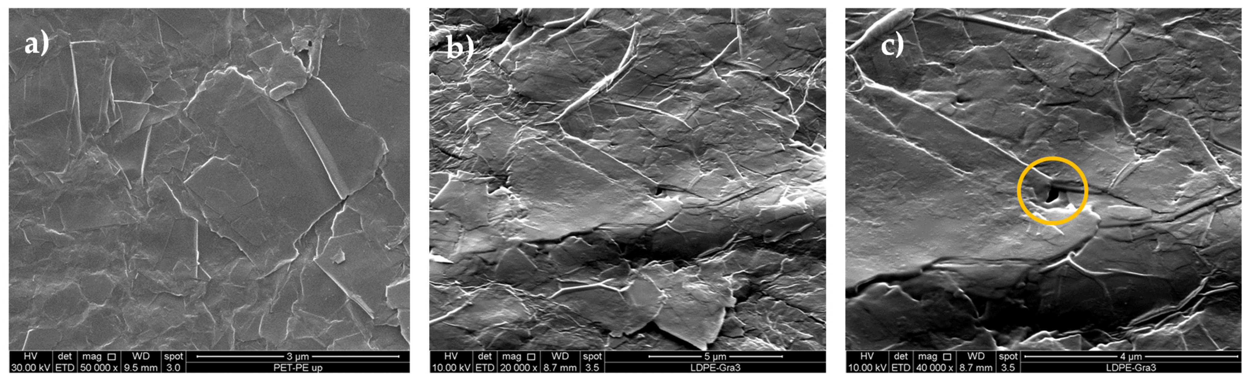
3.1. SEM Characterization of GNP Coatings on LD-PE

SEM micrographs of the sample surfaces of GNP spread on LD-PE films, imaged as the ‘top-view’ and ‘strongly-tilted view’, are compared in Figure 3. These SEM micrographs show that the sample surface is made of a continuous layer of graphite nanoplatelets. As shown, the number of grey levels in the tilted sample images (see Figure 3b,c) is much higher than in the case of the ‘top-view’ sample image (see Figure 3a), and this characteristic is capable of generating ‘light and shade’ effects, which are completely absent in the ‘top-view’ sample images.
Such a limited number of grey levels in the ‘top-view’ observations makes the microscopic features of the surface quite difficult to distinguish. In contrast, high-contrast images can provide a vast amount of topological information on the samples investigated. Indeed, the edges of graphite platelets appear white-colored (see Figure 3b,c), while the submerged areas in the same images appear dark and, in some cases, even black-colored. Instead, these submerged areas cannot be distinguished in the SEM micrographs showing the ‘top-view’ of the sample surface. In addition, these higher contrasted images allow one to easily distinguish structural elements present below the graphite platelet layer, and therefore, the SEM micrographs have a great wealth of morphological information. For example, the edge extension can be easily measured in these high-contrast images, defects like holes and pores become visible even in cases in which they have a very small size (see the yellow circle in Figure 3c), and fractures on the edges become clearly distinguishable.

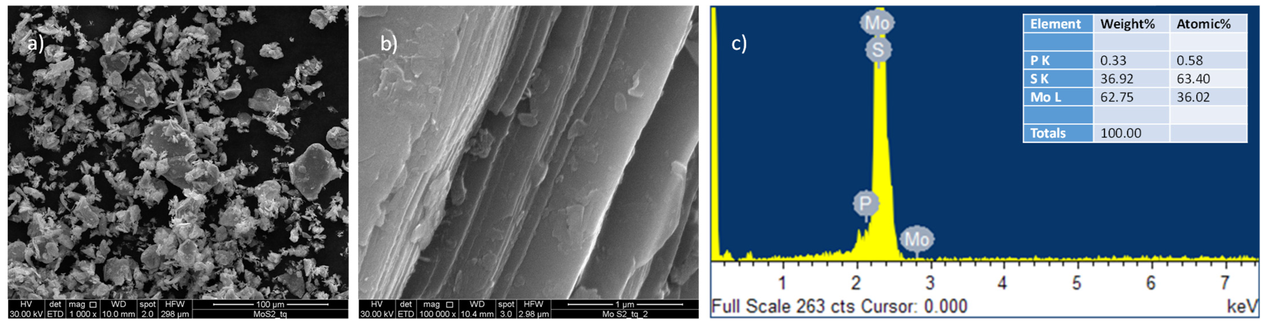
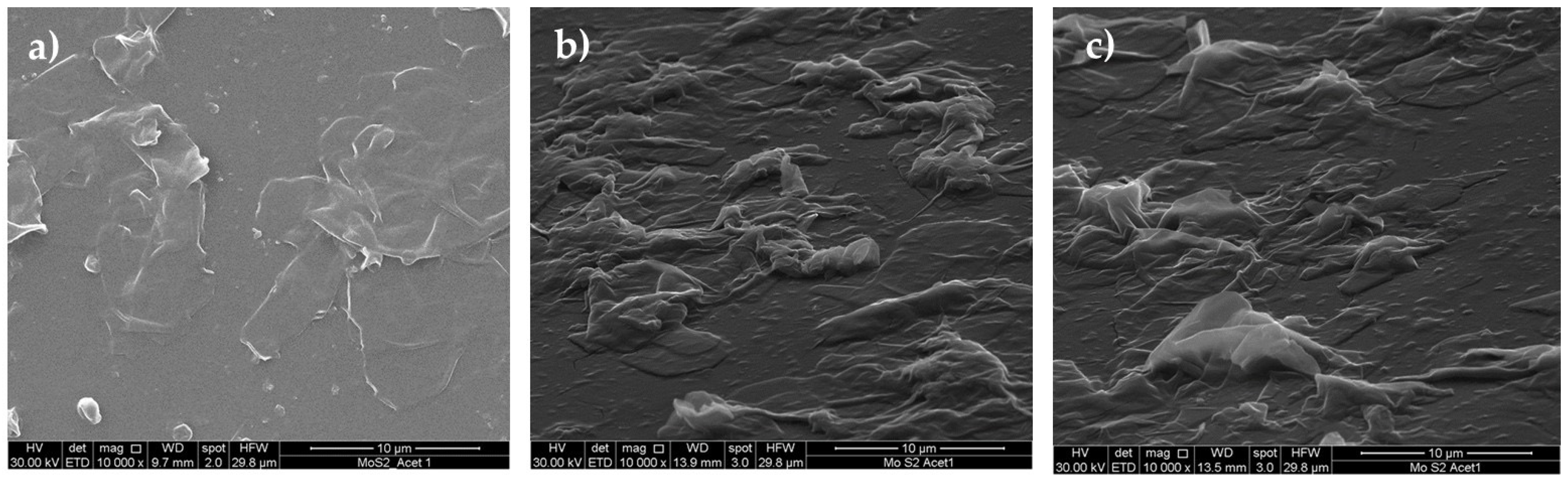
3.2. SEM-Characterization of MoS2 Coatings on Glass

The above considerations perfectly apply to 2D nanomaterials of a different nature. For example, Figure 4a–c shows the ‘top-view’ and the ‘strongly-tilted’ surfaces of a sample made of MoS2 on glass. Owing to the very small thickness of MoS2 single layers, the edges of these nanostructures cannot be clearly distinguished in the ‘top-view’ SEM micrograph of the sample (see Figure 4a). In contrast, the SEM micrograph of the ‘strongly tilted’ samples (see Figure 4b,c) clearly shows all features of this single-layer MoS2. For example, layer overlapping, ripples/folding in the layer, granular impurities, and many other types of defects in the nanostructures can be easily detected in these images.
Therefore, the proposed approach can be considered of general validity for the morphological characterization of 2D nanostructures.

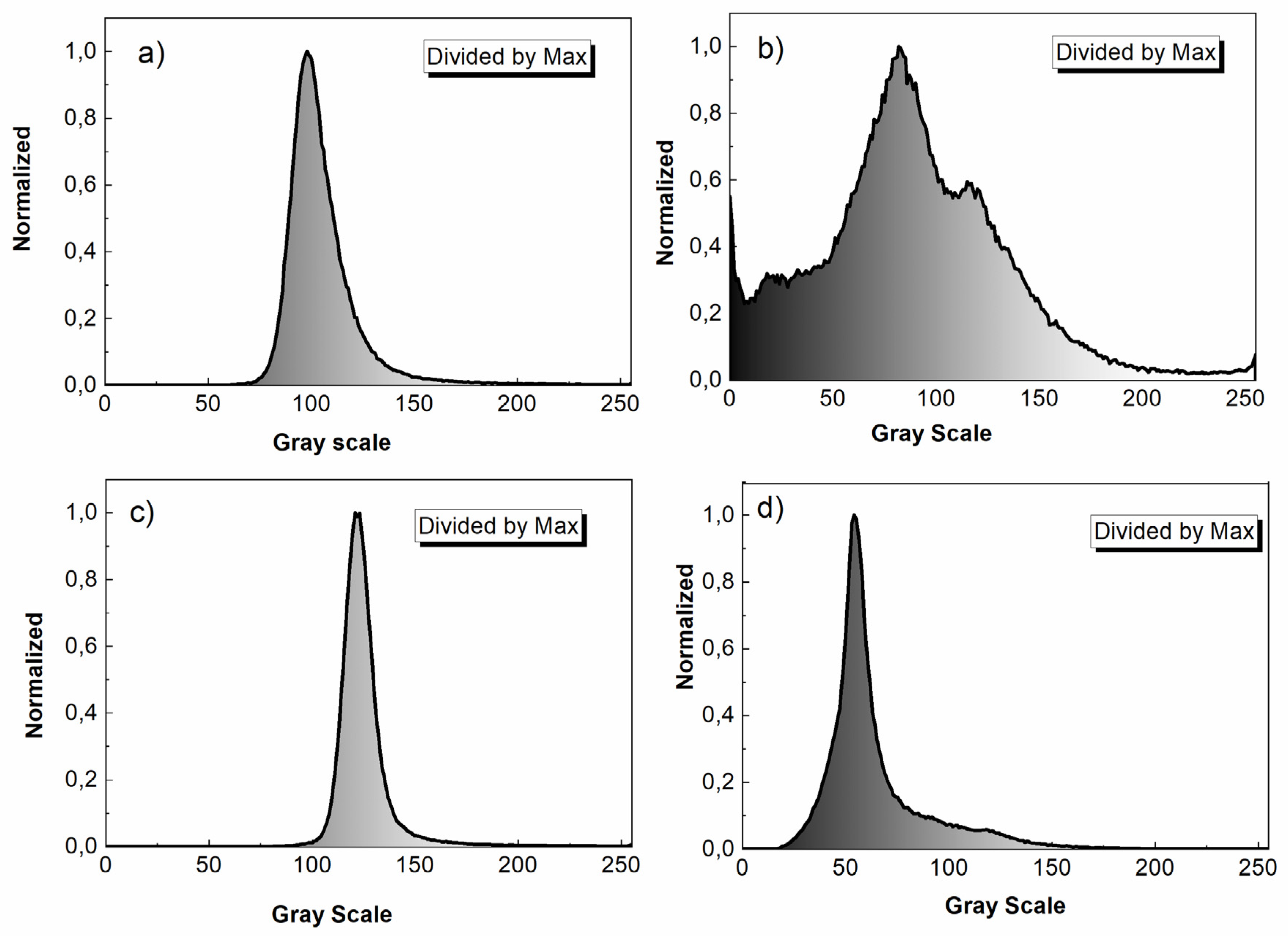
3.3. Quantitative Evaluation of SEM Image Contrast

The above visual considerations can be confirmed through image analysis of the SEM micrographs. Indeed, image analysis provides a quantitative evaluation of different grey levels present in these SEM micrographs. Grey levels in the micrographs of the ‘top-view’ and ‘strongly-tilted’ samples were analyzed with Image-J software, and the obtained results are shown in Figure 5. In order to make the sample SEM micrographs obtained with and without 90° tilting comparable, images containing the same number of pixels were analyzed by measuring the percentages of all grey levels present in the images. Then, the achieved histograms were normalized with respect to the maximum intensity (the intensity of the most abundant grey level present in the image). Such normalization allowed for the correct visualization of the number of grey levels present in each graph. The number of grey levels grew from 194 (Figure 5a) to 255 (Figure 5b), which corresponds to an increase of 31.4%. Since contrast enhancement also depends on the frequency of different grey levels, we measured the area below each curve, finding a 61.1% increase in this parameter. This same approach was applied to the micrographs of MoS2 coatings. Also, in this case, the normalization of the histograms allowed us to better visualize the grey levels present in each graph. The number of grey levels grew from 169 (Figure 5c) to 237 (Figure 5d), which corresponds to an increase of 40.2%. Also, in this case, we measured the area below each curve, finding a 30.1% increase in this area. Therefore, it is evident from such results that the 90° tilting operation significantly increases the image contrast.
In other words, the increase in contrast observed with a significant tilting of the 2D nanostructures (i.e., close to 90°) is due to the higher yield of SEs per PE, which results in a SE emission occurring in a region of the sample closer to the surface. In fact, SEs usually have low energy values, and therefore, they can escape the sample only in cases in which they are produced very close to the surface. An immediate sub-surface emission is achieved with the grazing incidence of the PE beam. In contrast, a vertical PE beam incidence causes SE emission from deep sample regions with consequent yield decrease.

4. Conclusions

The SEM observations of samples made of single-layer MoS2 deposited on glass and GNP-coated LDPE films have proven the capability of the tilting operation to significantly increase contrast in the micrographs. In particular, in order to maximize the sample surface tilting, specimens were vertically positioned by using an aluminum slotted specimen stub, and manual tilting was applied to achieve perfect focusing in the full image field. The SEM micrograph of the tilted samples had very good contrast characteristics, capable of allowing a clear visualization of all features of the deposited 2D nanostructures.

Author Contributions

Conceptualization, G.C.; investigation, G.C., A.L., and M.P.; data curation, A.L., M.P., and G.C.; writing—original draft preparation, A.L., M.P., and G.C.; writing—review and editing, A.L., M.P., F.G., and G.C.; project administration, F.G.; funding acquisition, F.G. All authors have read and agreed to the published version of the manuscript.

Funding

The authors acknowledge financial support provided by the National Recovery and Resilience Plan (NRRP), Mission 4, Component 2, Investment 1.1, Call for tender No. 1409 published on 14 September 2022 by the Italian Ministry of University and Research (MUR), funded by the European Union—NextGenerationEU—Project Title “Development of two-dimensional environmental gas nano-sensors with enhanced selectivity through fluctuation spectroscopy (2DEGAS)” Grant P2022S5AN8.

Institutional Review Board Statement

Not applicable.

Informed Consent Statement

Not applicable.

Data Availability Statement

The original contributions presented in this study are included in the article. Further inquiries can be directed to the corresponding author(s).

Acknowledgments

The authors are grateful to Maria Cristina Del Barone of Lamest laboratory—IPCB for their support during the SEM characterization.

Conflicts of Interest

The authors declare no conflicts of interest.

References

  1. Baig, N. Two-dimensional nanomaterials: A critical review of recent progress, properties, applications, and future directions. Compos. Part A Appl. Sci. Manuf. 2023, 165, 107362. [Google Scholar] [CrossRef]
  2. Tene, T.; Tubon-Usca, G.; Haro-Barroso, C.; Velasco Castelo, G.M.; Vacacela Gomez, C. Two-Dimensional Materials-Based Thin Films and Coatings. Coatings 2024, 14, 1242. [Google Scholar] [CrossRef]
  3. Satya Prasad, S.V.; Prasad, S.B.; Singh, S. Nanostructured 2D materials as nano coatings and thin films. In Advanced Applications of 2D Nanostructures. Materials Horizons: From Nature to Nanomaterials; Springer: Singapore, 2021; pp. 55–72. [Google Scholar] [CrossRef]
  4. Coscia, U.; Palomba, M.; Ambrosone, G.; Barucca, G.; Cabibbo, M.; Mengucci, P.; de Asmundis, R.; Carotenuto, G. A new micromechanical approach for the preparation of graphene nanoplatelets deposited on polyethylene. Nanotechnology 2017, 28, 194001. [Google Scholar] [CrossRef] [PubMed]
  5. Bonavolontà, C.; Aramo, C.; Valentino, M.; Pepe, G.P.; De Nicola, S.; Carotenuto, G.; Longo, A.; Palomba, M.; Boccardi, S.; Meola, C. Graphene–polymer coating for the realization of strain sensors. Beilstein J. Nanotechnol. 2017, 8, 21–27. [Google Scholar] [CrossRef] [PubMed]
  6. Srinivasan, A.; Han, W.; Zheng, M.; Khursheed, A. Characterization of materials using the secondary electron energy spectromicroscopy technique. Opt. Mater. X 2021, 12, 100121. [Google Scholar] [CrossRef]
  7. Shi, Q.; Roux, S.; Latourte, F.; Hild, F.; Loisnard, D.; Brynaert, N. Measuring topographies from conventional SEM acquisitions. Ultramicroscopy 2018, 191, 18–33. [Google Scholar] [CrossRef] [PubMed]
  8. Huang, L.; Zhang, D.; Zhang, F.H.; Huang, Y.D.; Gan, Y. Graphene to graphene, and substrate to substrate: How to reliably differentiate supported graphene from polycrystalline substrates using SEM? Mater. Res. Express 2019, 6, 085604. [Google Scholar] [CrossRef]
  9. Pachauri, V.; Kern, K.; Balasubramanian, K. Chemically exfoliated large-area two-dimensional flakes of molybdenum disulfide for device applications. APL Mater. 2013, 1, 032102. [Google Scholar] [CrossRef]
  10. Forsberg, V.; Zhang, R.; Bäckström, J.; Dahlström, C.; Andres, B.; Norgren, M.; Olin, H. Exfoliated MoS2 in water without additives. PLoS ONE 2016, 11, e0154522. [Google Scholar] [CrossRef] [PubMed]
Figure 1. SEM micrographs of commercial MoS2 (a,b) and its EDS spectrum with the elemental composition (c).
Engproc 87 00081 g001
Figure 2. Aluminum slotted specimen stub with a glass slide coated with MoS2.
Engproc 87 00081 g002
Figure 3. SEM micrographs showing the ‘top-view’ of a graphite coating (a) and the same sample after tilting from 90° (b,c). The yellow circle evidences a defect in the coating layer.
Engproc 87 00081 g003
Figure 4. SEM micrographs showing the ‘top-view’ of a MoS2 coating (a) and the same sample after tilting from 90° (b,c).
Engproc 87 00081 g004
Figure 5. Analysis of the grey levels in the SEM micrographs shown in Figure 3 and Figure 4. In particular, the analyses refer to the following: (a) Figure 3a; (b) Figure 3c; (c) Figure 4a; (d) Figure 4c.
Engproc 87 00081 g005
Disclaimer/Publisher’s Note: The statements, opinions and data contained in all publications are solely those of the individual author(s) and contributor(s) and not of MDPI and/or the editor(s). MDPI and/or the editor(s) disclaim responsibility for any injury to people or property resulting from any ideas, methods, instructions or products referred to in the content.

