Proceeding Paper

Verification of SoC Using Advanced Verification Methodology †

by
Pranuti Pamula
1,
Durga Prasad Gorthy
2,
Phalguni Singh Ngangbam
1 and
Aravindhan Alagarsamy
1,*
1
Multi-Core Architecture Computation (MAC) Lab, Department of ECE, Koneru Lakshmaiah Education Foundation, Vaddeswaram 522501, India
2
AMD, Hyderabad 500081, India
*
Author to whom correspondence should be addressed.
Presented at the International Conference on “Holography Meets Advanced Manufacturing”, Online, 20–22 February 2023.
Eng. Proc. 2023, 34(1), 12; https://doi.org/10.3390/HMAM2-14160
Published: 13 March 2023

Abstract

:
The semiconductor industry has evolved significantly since its founding in 1950. Transistors and diodes are the primarily used electronic devices, but advancements in technology have led to more complex semiconductor devices, from printed circuit boards to multimillion gate design, i.e., a System on Chip (SoC) design. Almost 70–80 percent of the total SoC design effort is aimed at functional verification. In this paper, verification of an interconnect block in a processing system is presented. Trace monitoring of the transactions on the Advanced eXtensible Interface (AXI) interface of the interconnect is performed by programming different operational pointers and filters. Results were simulated from Synopsys—a Verilog Compiler Simulator (VCS) tool-2022v (Hyderabad, India).

1. Introduction

In recent years, the complexity of System on Chip (SoC) design has increased. The higher number of components in a single chip makes the verification of any SoC design very critical. Hence, a proper methodology for any SoC or IP is required [1,2,3,4]. Despite all the advancements, there is a significant gap between the modern technology and the verification needs of new industries. This situation is becoming worse regarding to the change in design as there is rapid movement towards the era of automated vehicles, smart cities and the Internet of Things (IoT) [5,6,7,8]. Moreover, these electronic devices collect personal information such as location, sleep patterns, health, etc., which is stored in the billions of computer devices that operate without pause and even the surrounding environment may have compromised or malicious devices. As the system design and security have transformed to adapt themselves, so must the verification adjust as well. Regarding the growing requirements for the design and the time to market, the duration has shrunk from years required for verification and hard work to less than a year. This aggressive shrinking implies shorter timespan for a thorough design review, which may cause misunderstanding of the requirements and a consequent increase in errors. Therefore, verification is expected to handle more errors in design with even less time duration.

Problem Statement

Verification of an SoC design is carried out at different stages with a different approach as per design specifications. With interconnect as a common ground for all the rest of the design to interact, there are many functionalities to be verified and connectivity checks to be conducted. Many tests need to be developed for the verification of an interconnect. Connectivity checks at the interface interconnect being the most important requires detailed analysis and thorough research of the design specification. Track sourcing from the primary interface should reach the desired secondary interface without any loss in the data packets, such checks between multiple primary and secondary interfaces are carried out by initiating write operations to a register space of the secondary interface and expecting to read the same data without any errors. These transactions can be self-tested using System Verilog assertions and checkers. The other functionalities of the design can be verified with a variety of approaches.

2. Materials and Methods

Deep sub-micron effects complicate design closure for very large designs [9]. A System on Chip (SoC) is an IC (Integrated Circuit) which is designed by integrating multiple standalone VLSI designs that provide complete functionality for an application. SoC integrates a microprocessor with advanced peripherals such as a coprocessor, memory elements, GPU, Wi-Fi module, etc. This definition of SoC emphasizes the predesigned models of complex design functions which are known as cores. These can be intellectual property blocks, virtual components, macros, etc. In SoC, in-house library cores may be used along with some cores designed by other design houses known as intellectual property. Because of the use of the embedded software and the increasing integration of cores, the design complexity of SoC has increased dramatically over the past few years. In addition, it is still expected to grow at a very fast rate. According to Moore’s law, silicon complexity quadruples every three years [10]. This complexity accounts for the huge size of cores and shrinking geometry.
There are three types of SoCs that are totally distinguishable, i.e., a SoC built around a micro-controller, a SoC built around a microprocessor, and a programmable SoC, where the internal elements are not predefined and can be programmed in any essential manner. These kinds of SoCs are also known as FPGAs or complex programmable logic devices. In all SoC designs, predefined cores are the essential components. The flexibility of the cores depends on the form in which they are available. The trade-off between these cores is in terms of performance, power, speed, area, flexibility, cost, time to market, etc. [11].

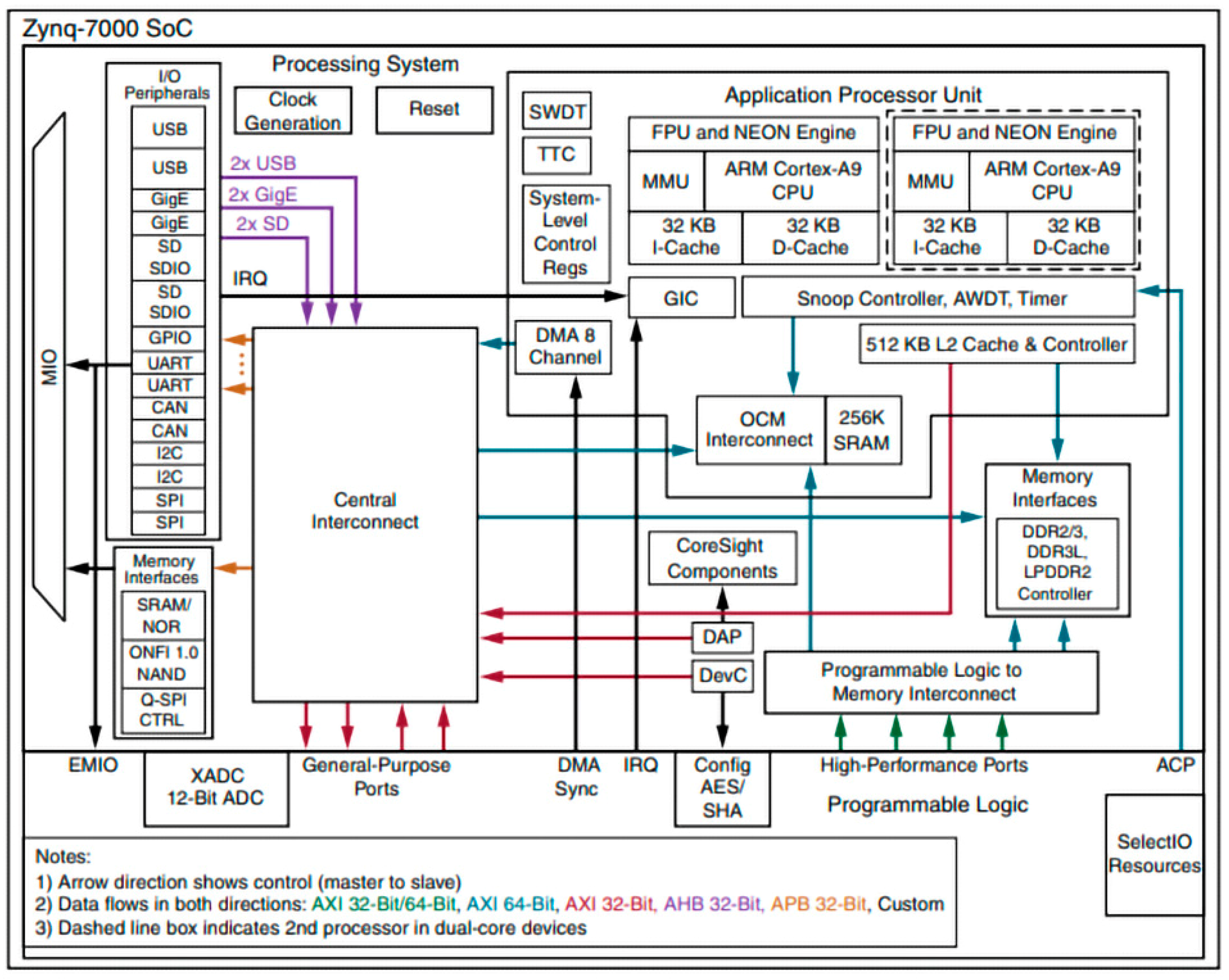
2.1. Architectural Overview

The SoC architecture integrates a feature of a dual- or single-core microprocessor core-based processing system and a Xilinx programmable logic in a single device. It is built on state-of-the-art technology that offers high performance and low power [12]. The multi-core processors are the heart of the PS, which also includes on-chip memory, external memory interfaces, and a rich set of I/O peripherals.
SoC offers the flexibility and scalability of an FPG, while providing performance, power, and ease of the use. The range of devices in the family of SoC enables the designers to find cost-sensitive as well as high-performance applications from a single platform using standard tools.
Functional blocks of SoC are shown in Figure 1. The processing system and programmable logic both operate on different power domains. This configuration enables the users to manage the power utilization of PL if required.
The SoC is composed of two major functional blocks:
  • Processing system;
  • Programmable logic.

Processing System (PS)

  • Application processor unit: The application processor unit offers high performance and standard-compliant capabilities. The runtime configurations allow the single processor or asymmetrical or symmetrical multiprocessing setups. It is a 32 Kb instruction set with a 32 Kb cache [12]. In addition, a sharable 512 Kb cache with parity is available. An accelerator coherency port from PL to PS, which is a 64 b AXI slave port, provides a connection between the processing system and programmable logic. APU also contains 256 Kb of on-chip SRAM which is a dual-ported memory. It is accessible to CPUs, PL, and central interconnects. There are four DMA (direct memory access) channels for PS to copy data from CPU memory to/from other system memories.
  • Memory interfaces: The memory interface of PS includes multiple memory technologies. It consists of DDR controllers with 16 b and 32 b widths. This uses up to 73 dedicated pins of PS [12]. The DDR can be powered down as per the idle periods of PS. Transaction scheduling is performed for optimizing data bandwidth and latency. The efficiency of memory is increased by 90% by advanced re-ordering engines and increased by 80% with random read/write operations. Collision check monitors the memory for any write–read collisions and the write buffer is used in that case. The primary boot device can be a NAND controller or a parallel SRAM/NOR controller.
  • I/O peripherals: The input–output peripherals are a collection of industry standard interfaces for communication with external systems. Programmable interrupt controllers on the GPIO are used for a status read of raw and masked interrupts. These interrupts are positive-edge, negative-edge, either--edge, high-level, or low-level sensitive. A USB 2.0 high-speed on-the-go (OTG) dual-role USB host controller and USB device controller operations are performed using a single hardware. This configuration uses MIO pins only. The USB host controller registers, and data structures are EHCI compatible [12]. It supports up to 12 endpoints.
  • Interconnect: The SoC uses several interconnect technologies that are optimized for specific communication requirements of the functional blocks. The SoC interconnect is divided into two parts: one is based on the high-performance data path of AXI on the PS interconnect and the other is based on PS-PL interfaces. The PS interconnect consists of an OCM interconnect and a central interconnect. The OCM interconnect provides access to 256 Kb of memory from the central interconnect and PL. The CPU and ACP interfaces have the lowest latencies to OCM through the SCU. The central interconnect is a 64-bit interconnect. It connects the input–output peripherals and the DMA controller to the DDR memory controller, on-chip RAM, and the AXI-GP interfaces for PL logic. It also connects the local DMA units in Ethernet, USB, and SD/SDIO controllers to the central interconnect. It also connects the PS master to the IOP.

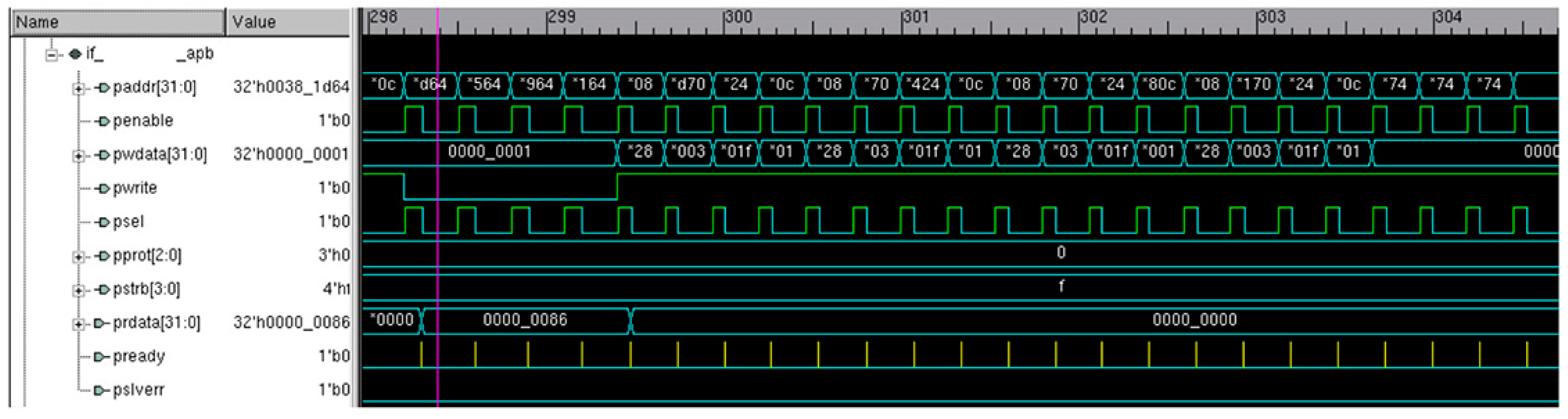
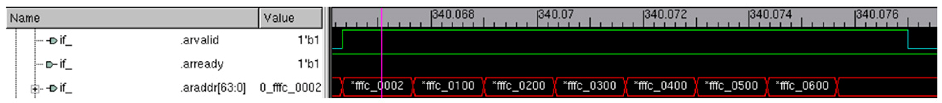
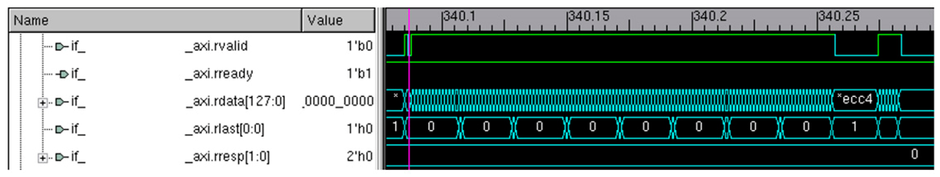
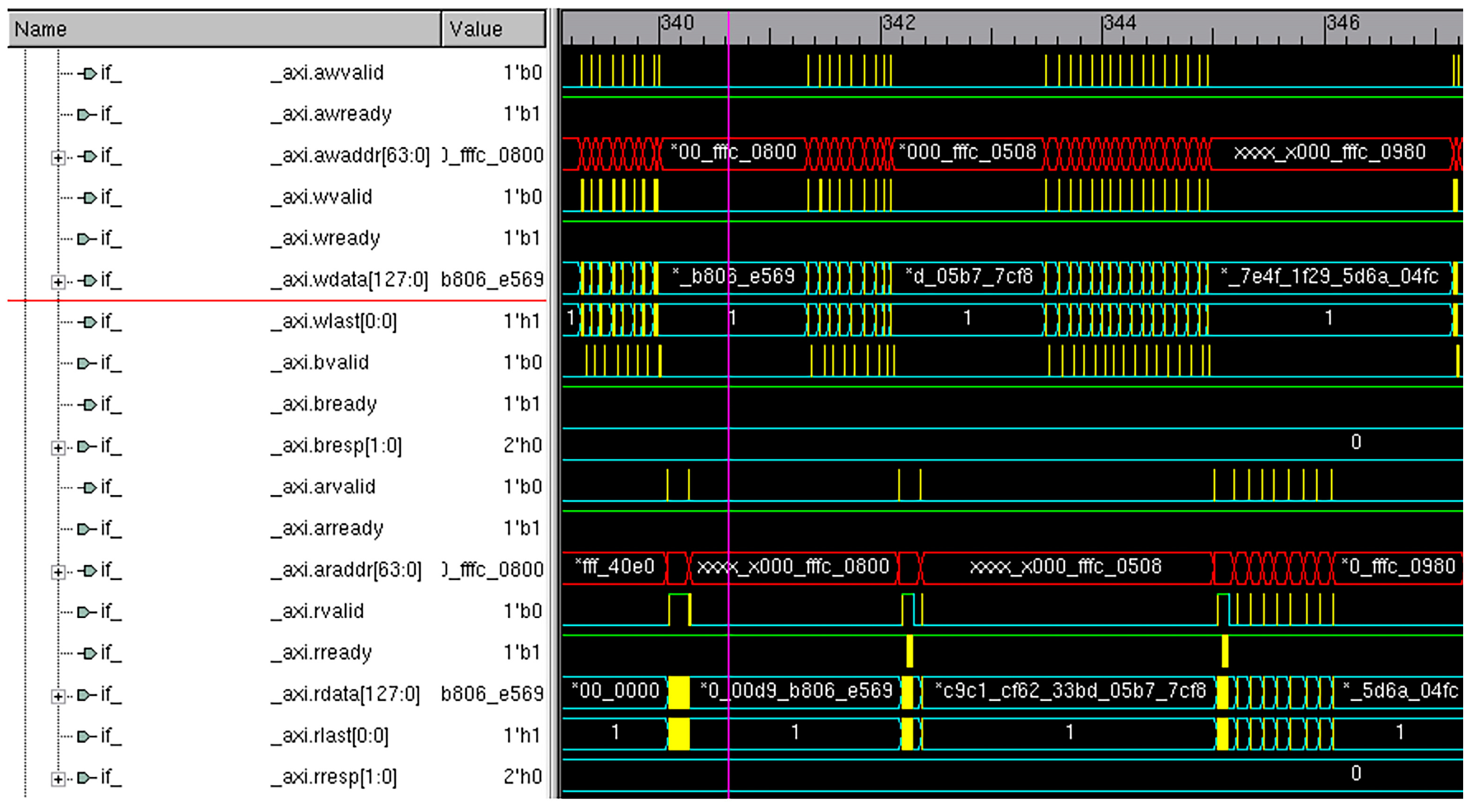
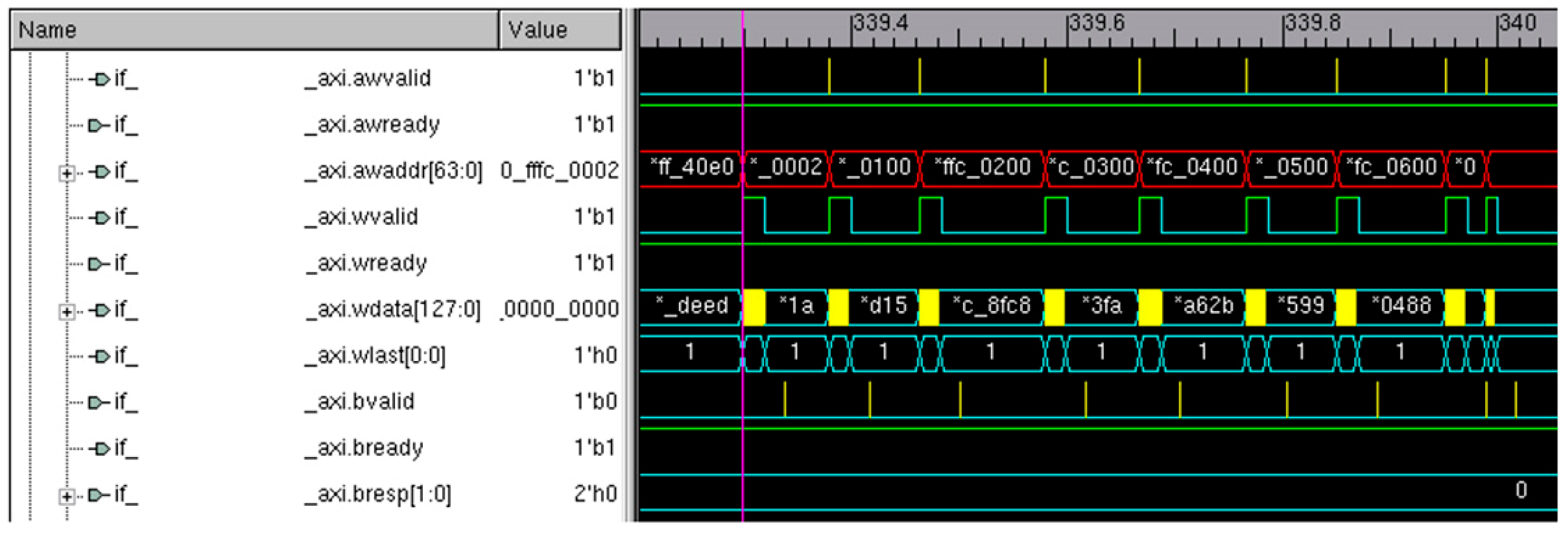
2.2. Connectivity Check in Interconnect
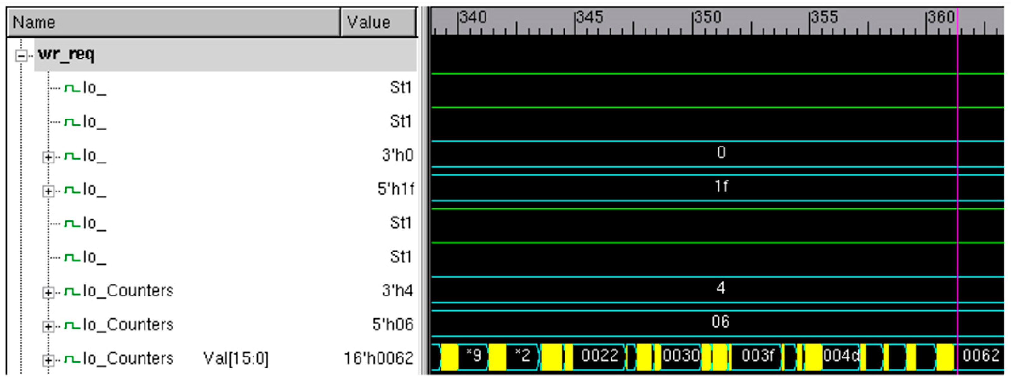
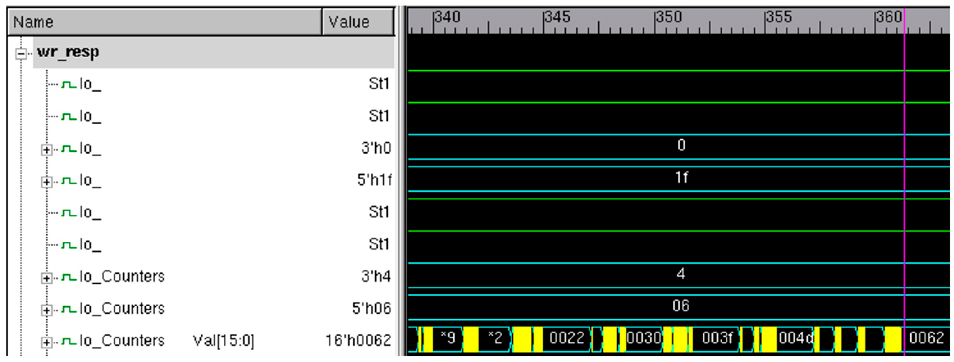
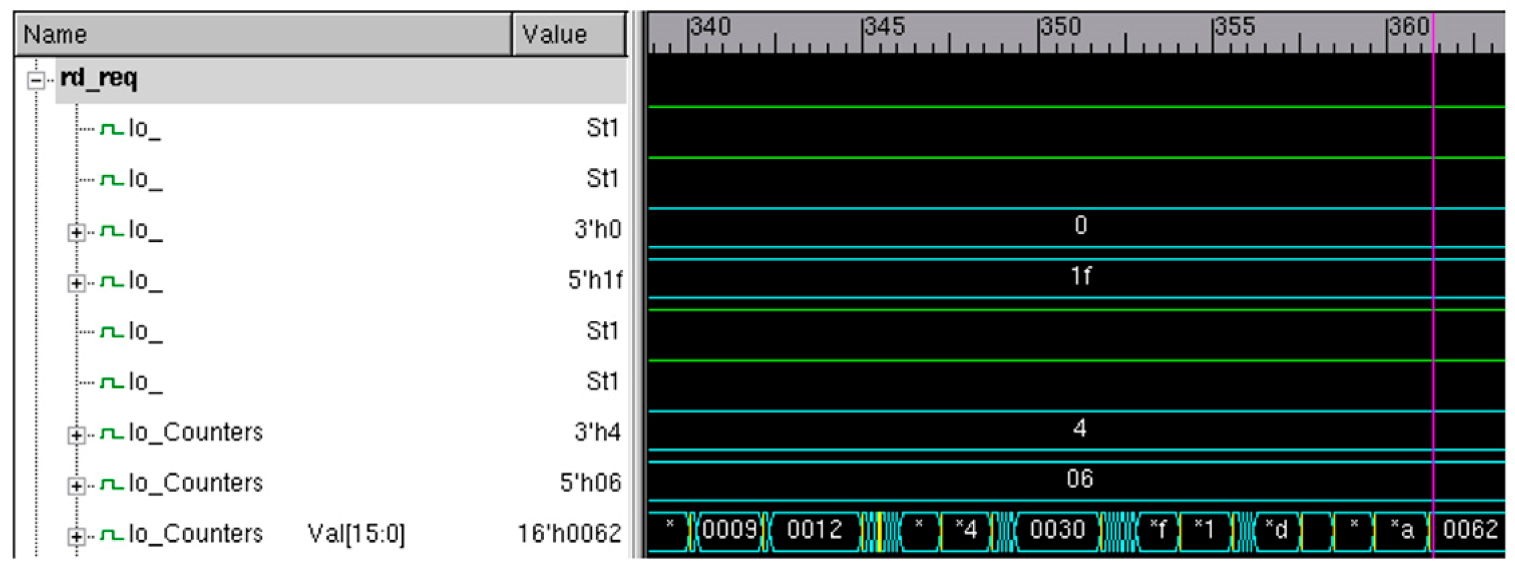
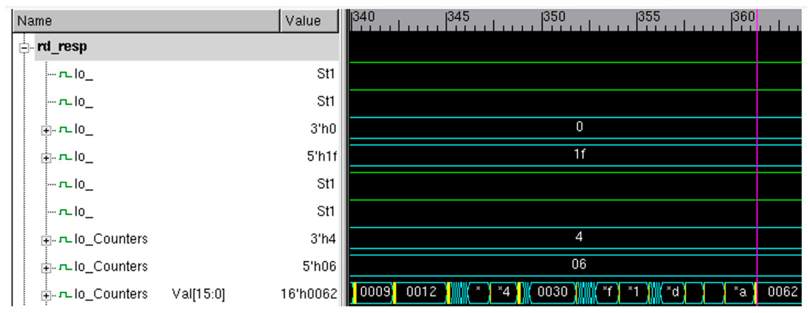
Interconnect consists of several input and output interfaces. Each of the interfaces reaches out to different slave modules or input from connected masters. The connectivity checks are essential at every interface. This is performed to verify the transactions that are intended to pass through a particular interface are reaching without any loss of data packets. Such checks are carried out by initiating from a master to register space of slave and expect to read exactly the same data without any errors. This behavior of the design is verified by using the system Verilog Assertions and data comparison using C or System Verilog [13]. The analysis of the simulated result is as important as defining the sequence of the test. The occurrence of an error or unexpected behavior at the output is required to be traced back to the source of the issue. A large amount of time is spent on debugging of simulated results. One of the test scenarios generated to verify connectivity at an interface is as discussed. The simulation result for verification of an AXI interface and APB interface are shown in the waveforms.

3. Results

Verification of blocks is of utmost importance. This is achieved by programming a testbench to monitor outgoing traffic with the help of pointers. This outgoing traffic can contain a large bandwidth of data signals. These outgoing data can be filtered as per the requirement and a trace can be generated for only those selected data signals or transactions. The pointers required to monitor the interface are programmed using a set of control registers. These configurations are shown in Figure 2.
When pointers are configured and set to monitor a port, the filters are activated to filter out the required amount of data. The filters are configured as per the address or ID of the transactions and later subdivided by control/instruction trace, data trace, bus trace, interface trace, fabric trace, etc. Then, a burst of AXI transactions is sent to the observed port. A set of such transactions is displayed in Figure 3, Figure 4 and Figure 5.
The write and read burst transfers sent to the AXI bus are shown in Figure 6. The above image shows traffic sent to the observed port. These transactions are then observed with the help of pointers. The transactions on the interface are filtered and sent out to the counter, to count the number of transaction hits. The output is thus observed and analyzed for verification.
Below are the waveforms depicting the counter values at the output. The output of the write request pointer is shown in Figure 7.
The output of the write response pointer is shown in Figure 8.
The output of the read request pointer is shown in Figure 9.
The output of the read response pointer is shown in Figure 10.
  • Green line: Transaction of 1.
  • Blue line: Transaction of 0.
  • Yellow line: Brust Transactions.
  • Purple line: Marker.
  • Red line: transaction of address is represented.

4. Conclusions

SoC verification is a complex and never-ending task. The process can be faster and more efficient when proper programming and simulation tools are used. Verification can be achieved with prior knowledge of SoC architecture and RTL design, where the environment is built using UVM and System Verilog. All the parts of the testbench can be reused easily for different designs. This reduces verification complexity and improves efficiency. The design functionalities are verified by using assertions and checkers along with the basic test sequence.
The connectivity of an interconnect block with several interfaces is verified successfully. The performance monitoring at various interfaces of interconnect is successfully completed. The simulation results are compared and evaluated by a self-checking testbench. This reduces extra efforts to locate the problem or issue in the design, as it locates the exact timestamp and points at the exact line of the RTL code where a violation has occurred.

Author Contributions

A.A.: Conceptualization, methodology, software, investigation, writing—original draft, funding acquisition, project administration; P.P.: Methodology, formal analysis, writing—original draft; D.P.G.: Investigation, software, resources; P.S.N.: Supervision. All authors have read and agreed to the published version of the manuscript.

Funding

A.A.: P.P.: P.S.N.: The first authors thanks DST-FIST for funding the lab facility for supporting this research under grant number SR/FST/ET-II/2019/450.

Institutional Review Board Statement

Not applicable.

Informed Consent Statement

Not applicable.

Data Availability Statement

No data was used for the research described in the article.

Conflicts of Interest

The authors declare that they have no known competing financial interest or personal relationships that could have appeared to influence the work reported in this paper.

References

  1. Ghosh, P.; Srivastava, R. Case Study: SoC Performance Verification and Static Verification of RTL Parameters. In Proceedings of the 2019 20th International Workshop on Microprocessor/SoC Test, Security and Verification (MTV), Austin, TX, USA, 9–10 December 2019; pp. 65–72. [Google Scholar]
  2. Huang, X.; Liu, L.; Li, Y.; Liu, L.; Huang, X. FPGA Verification Methodology for SiSoC Based SoC Design. In Proceedings of the 2011 IEEE International Conference of Electron Devices and Solid-State Circuits, Tianjin, China, 17–18 November 2011. [Google Scholar]
  3. Bai, L.; Fan, X.; Zhang, M.; Sun, L. A VMM/FPGA Co-verification Method for “Longtium Stream” Processor. In Proceedings of the 2013 IEEE International Conference on Signal Processing, Communication and Computing (ICSPCC 2013), KunMing, China, 5–8 August 2013. [Google Scholar]
  4. Podivinsky, J.; Simkova, M.; Cekan, O.; Kotasek, Z. FPGA Prototyping and Accelerated Verification of ASIPs. In Proceedings of the 2015 IEEE 18th International Symposium on Design and Diagnostics of Electronic Circuits & Systems, Belgrade, Serbia, 22–24 April 2015; pp. 145–148. [Google Scholar]
  5. Noami, A.; Alahdal, A.; Kumar, B.P.; Chandrasekhar, P.; Safi, N. High Speed Data Transactions for Memory Controller Based on AXI4 Interface Protocol SoC. In Proceedings of the 2021 International Conference on Advances in Electrical, Computing, Communication and Sustainable Technologies (ICAECT), Bhilai, India, 19–20 February 2021. [Google Scholar]
  6. Seongyoung, S.; Moon, J.; Jun, S. FPGA-Accelerated Time Series Mining on Low-Power IoT Devices. In Proceedings of the 2020 IEEE 31st International Conference on Application-specific Systems, Architectures and Processors (ASAP), Manchester, UK, 6–8 July 2020. [Google Scholar]
  7. Noami, A.; Kumar, B.P.; Paidimarry, C.S. Power Optimization for Multi-Core Memory Controller Using Intelligent Clock Gating Technique. J. Electr. Electron. Eng. 2022, 15, 129–137. [Google Scholar]
  8. Gophane, K.C.; Bhaskar, P.C. FPGA Based Adaptive IoT Framework for Distinct Applications. In Proceedings of the 2018 Fourth International Conference on Computing Communication Control and Automation (ICCUBEA), Pune, India, 16–18 August 2018. [Google Scholar]
  9. Accounting For Very Deep Sub-Micron Effects in Silicon Models. Available online: https://www.eetimes.com/accounting-for-very-deep-sub-micron-effects-in-silicon-models/ (accessed on 15 February 2023).
  10. Tuomi, I. The lives and death of Moore’s Law. First Monday 2002, 7. [Google Scholar] [CrossRef]
  11. Noguera, J.; Badia, R.M. System-level power-performance trade-offs in task scheduling for dynamically reconfigurable architectures. In Proceedings of the 2003 International Conference on Compilers, Architecture and Synthesis for Embedded Systems, San Jose, CA, USA, 30 October–1 November 2003. [Google Scholar]
  12. Zynq-7000 SoC Data Sheet: Overview. Available online: https://docs.xilinx.com/v/u/en-US/ds190-Zynq-7000-Overview (accessed on 15 February 2023).
  13. Chris, S. System Verilog for Verification: A Guide to Learning the Testbench Language Features; Springer Science & Business Media: Berlin/Heidelberg, Germany, 2008. [Google Scholar]
Figure 1. SoC architecture.
Engproc 34 00012 g001
Figure 2. Configuration of pointers.
Engproc 34 00012 g002
Figure 3. Write operation of the AXI burst transfer.
Engproc 34 00012 g003
Figure 4. Read operation of the AXI burst transfer.
Engproc 34 00012 g004
Figure 5. Read response on the AXI burst transfer.
Engproc 34 00012 g005
Figure 6. Burst traffic on the AXI interface.
Engproc 34 00012 g006
Figure 7. Write request transfers.
Engproc 34 00012 g007
Figure 8. Write response transfers.
Engproc 34 00012 g008
Figure 9. Read request transfers.
Engproc 34 00012 g009
Figure 10. Read response transfers.
Engproc 34 00012 g010
Disclaimer/Publisher’s Note: The statements, opinions and data contained in all publications are solely those of the individual author(s) and contributor(s) and not of MDPI and/or the editor(s). MDPI and/or the editor(s) disclaim responsibility for any injury to people or property resulting from any ideas, methods, instructions or products referred to in the content.

