Abstract
Millimeter-wave (mm-wave) radar has become a key technology in wireless sensor networks (WSNs) due to its high spatial resolution and penetration capability, enabling applications such as smart traffic control and non-contact health monitoring. Achieving fine-range resolution necessitates wide signal bandwidth, which places stringent demands on power amplifier (PA) performance in terms of bandwidth, efficiency, and output power. Therefore the design of the power amplifier for WSN poses significant challenges. This paper presents a broadband mm-wave PA implemented in a 40 nm CMOS process, utilizing transformer-based power combining to enhance efficiency and bandwidth simultaneously, which can adequately meet the requirements of WSN systems. The PA achieves a 3 dB flat power bandwidth up to 62% from 13 to 24.8 GHz. At 19 GHz, it delivers a saturated output power (Psat) of 12.3 dBm, a 1 dB compression point (P1dB) of 10.15 dBm, and exhibits a peak power-added efficiency (PAE) of 23%, with 17.2% PAE at P1dB. The PA consumes 43 mW from a 1.1 V supply and occupies an active area of only 0.06 mm2. These results validate the effectiveness of transformer-based combining for achieving compact, high-performance broadband PAs in CMOS, and demonstrate its suitability for mm-wave radar systems requiring high-range resolution. The amplifier provides a high stability, with output return losses better than −10 dB.
1. Introduction
Monitoring of breathing and heart rate forms the foundation for a wide range of medical, health, and safety applications. Continuous and real-time monitoring enables doctors and automated systems to detect early signs of disease, monitor post-surgical recovery, and assess the health status of elderly patients living alone. It is also essential for tracking stress levels, sleep quality, and other physiological parameters in healthy individuals. Traditional methods rely on chest straps, adhesive electrodes (ECG), or photoplethysmography (PPG) sensors placed on the skin. While these systems are accurate, they have inherent limitations: they require physical contact, may cause skin irritation during prolonged use, and may interfere with normal activities. For long-term monitoring, especially for the elderly or infants, these devices are inconvenient and sometimes impractical. Therefore, the use of non-contact, high-precision millimeter-wave radar in wireless sensor networks (WSNs) has become a major focus of modern research [1]. Compared to Continuous-Wave (CW) radar and Ultra-Wide-Band (UWB) radar, Frequency-Modulated Continuous-Wave (FMCW) radar has lower costs and higher signal-to-noise ratios [2,3].
Figure 1 shows a wireless sensor network system for physiological monitoring. In this system, the RF front end uses a voltage-controlled oscillator (VCO) to generate an FMCW signal, which is then amplified by a power amplifier (PA) and transmitted by the transmit antenna. The target reflection signal is received by the receiving antenna and transmitted to the low-noise amplifier (LNA). Subsequently, the amplified signal is mixed with the original LO signal to generate an intermediate frequency (IF) signal, which is then sampled by the ADC and sent to the data processing center, ultimately transmitted to the PC.
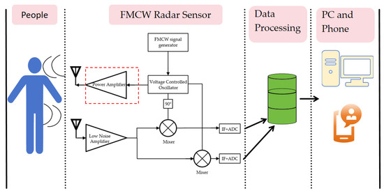
Figure 1.
Wireless sensor network system.
In conclusion, in FMCW radar, the PA is mainly responsible for enhancing the power of the transmitted signal. The output power, efficiency, and bandwidth of the PA have a significant impact on the performance of the radar. The reference [4] proposes a three-stage PA architecture using neutralizing capacitor technology, which has high gain but requires a DC current exceeding 100 mA, failing to meet low power requirements. Reference [5] presents a Q-band balanced medium-power amplifier. This balanced amplifier consists of two broadband amplifiers and two broadside couplers, achieving a 3 dB bandwidth of 35–51 G. However, its PAE is only 8%, it may generate heat in some wearable devices, and the chip area is 0.72 mm. Another challenge in PA design is how to enhance the saturated output power and bandwidth of PAs. Reference [6] adopts a magnetic coupling resonator (MCR) matching network to achieve wideband impedance transformation. The bandwidth of this PA is 63.3%, covering the entire Ka band range from 21.6 GHz to 41.6 GHz and achieving high-bandwidth performance in a 65 nm CMOS process. Reference [7] use a 1:2 Capacitance-Ratio-Equivalent Power Combiner to significantly increase the output power, and its saturated output power reaches 20 dBm.
In order to solve the previously mentioned problems, we propose a broadband power amplifier chip with high PAE and low power consumption. This chip can be used as part of a sensor in smart cities and health monitoring. It can not only meet the high output power required for non-contact millimeter-wave radar, but also satisfy the low-power consumption requirements of wearable medical monitoring devices. Thoracic changes caused by human respiration are approximately 5–12 mm, and the wide bandwidth of the PA improves resolution and accurately separates thoracic micromovements from background clutter.
2. Design of the Proposed Power Amplifier
The PA schematic includes the power amplifier core circuit, bias circuit, and output matching transformer. The core circuit of the power amplifier is the heart of the entire system, responsible for amplifying the input signal to generate the required output power. This paper adopts a differential structure and uses neutralization capacitor technology. The bias circuit is used to provide the transistor with an appropriate DC operating point to ensure it operates in the best state, thereby improving the linearity and stability of the amplifier. The output matching transformer is used to achieve the synthesis of the two PA power amplifiers and broadband matching.
Figure 2 shows the complete PA schematic proposed in this paper. The PA is designed in a 40 nm CMOS process and consists of two differential amplifier stages. Both stages use neutralization capacitors to improve gain, reverse isolation, and stability. The two-stage amplifier circuit is combined through a transformer to increase the maximum output power.
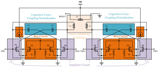
Figure 2.
The complete schematic of the proposed PA.
2.1. Core Circuit Design
Detailed simulation of the transistor to obtain the relationship between the threshold voltage Vth of the transistor and temperature changes. In order to reduce the circuit affected by temperature changes, instead of adopting a direct voltage bias, current injection into the transistor to generate a bias is used. Figure 3 shows the bias circuit.
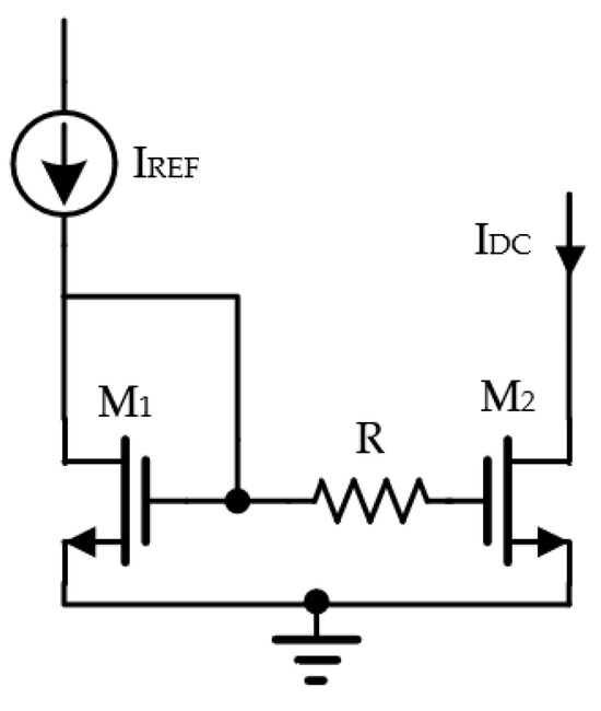
Figure 3.
The schematic of the bias circuit.
The IREF and IDC is given by (1) and (2):
where and represent the current flowing through the bias tube and amplifier tube , respectively. is the size of transistors and . is the overdrive for and ; since = , we can get the expression of :
From Equation (3), it can be observed that IDC is independent of Vth, so it is less affected by temperature.
In the millimeter-wave frequency band, the gate-drain parasitic capacitance Cgd significantly increases and cannot be ignored. The presence of Cgd creates a feedback loop between the gate and drain of the transistor, thereby reducing the maximum stable gain of the amplifier and degrading its stability and reverse isolation. To address this issue, cross-coupled neutralizing capacitance technology can be introduced into the differential amplifier, which is shown in Figure 4. A neutralizing capacitance Cc is connected between the gate of the transistor and the drain of its differential transistor. When the neutralizing capacitance Cc is equal in magnitude to the gate-drain capacitance Cgd, stability and reverse isolation are optimal. This technique not only enhances the stability of the PA and reduces the risk of self-oscillation but also ensures that the gain of each amplifier stage remains relatively independent. It isolates the impact of the matching pair in the subsequent amplifier stage on the preceding stage, thereby simplifying the overall amplifier design.
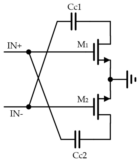
Figure 4.
Capacitive cross-coupling neutralization.
2.2. Coupled Resonant Cavity Broadband Matching
Figure 5 shows a magnetically coupled resonator. The use of transformer matching in the millimeter-wave frequency band has significant advantages. Under the condition that the area remains unchanged, transformer matching can provide higher-order networks and more design freedom.
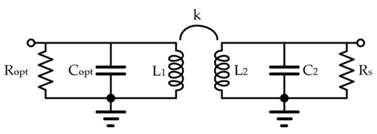
Figure 5.
Magnetically coupled resonator.
With loadpull simulation, we can get the optimal output impedance of the PA. Since ≈ , we use a symmetrically coupled resonant cavity, so that = and = :
Here, is not the operating frequency , and the relationship between the two is as follows:
Here is not the operating frequency , and the relationship between the two is as follows:
The no-gain ripple condition is as follows:
Using (4)–(6), Q is calculated as follows:
The desired coupling coefficient k is
in which
The inductance of the left resonator can be calculated using the following equation:
Again, the symmetry condition of the coupled resonant cavity leads to
2.3. Transformer-Based Power-Combining Technique
Due to the limitations of the CMOS process, it is still difficult to achieve a large output power in the millimeter-wave band with a single amplifier, and at this point, multiple amplifiers can be considered for power synthesis. Theoretically, doubling the number of synthesized circuits can increase the output power by 3 dB, but in practice, too many circuits will increase the loss of the synthesis network, and at the same time, the electromagnetic coupling of the synthesis network becomes more complicated, which reduces the synthesis gain significantly. Therefore, in this design, only a two-channel parallel synthesizer is used. In order to make the load impedance at the drain terminals of the two amplifiers highly consistent, reduce signal mismatch and improve the power synthesis effect. This paper designs a highly symmetrical transformer. The layout structure is shown in Figure 6.
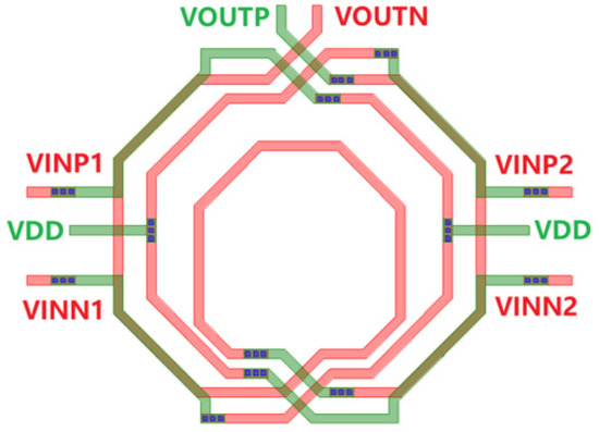
Figure 6.
Transformer layout structure.
3. Design Results
The layout of the proposed LNA, as shown in Figure 7.
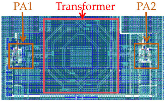
Figure 7.
Layout of PA.
We input a 19 G signal range from −15 dBm to 8 dBm and obtain a series of outputs from PA. Figure 8 shows the output power, the power gain, and PAE. The pink line is the output power, the red line is the power gain, and the blue line is PAE. The broadband PA achieves a saturated output power of 12.3 dBm with 23% PAE, and a 1 dB compression point of 10.15 dBm with 17.2 PAE.
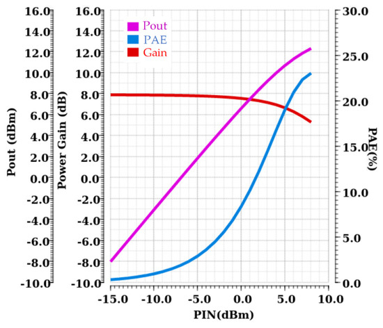
Figure 8.
Output power, power gain, and PAE.
The wider the bandwidth of the PA, the higher the resolution of millimeter-wave radar, and the more accurate the detection of chest cavity movement will be. We set the frequency or input signal range from 12 G to 28 G. And we obtain a 3 dB bandwidth of the PA up to 62% from 13 G to 24.8 G. Figure 9 shows the Psat as a function of frequency under different process corner and temperatures. Table 1 compares the PA designed in this paper with related published papers.
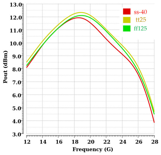
Figure 9.
Output power over frequency under different conditions.

Table 1.
Performance summary and comparison with different PAs.
4. Conclusions
This paper presents a PA circuit that can be applied in wireless sensor networks, utilizing 40 nm CMOS process. This PA employs neutralizing capacitor technology to address stability challenges and uses a transformer for power synthesis to achieve high output power. The chip area is only 0.06 , achieving a 3 dB bandwidth of 62% under TT process. With a power consumption of just 43 mW, it delivers an output of 12.3 dBm, while the PAE reaches 23%, demonstrating excellent efficiency. Additionally, the P1dB is 10.15 dBm, indicating high linearity. Performance remains stable across different process angles. For example, in health monitoring applications, the proposed PA meets the low power and high efficiency requirements of wearable medical monitoring devices while also fulfilling the high output power demands of non-contact radar sensors. Similarly, in fields such as smart city and transportation systems, the PA also showing better prospects.
Author Contributions
Conceptualization, Y.W. and J.C.; methodology, Y.W. and J.C.; software, Y.W.; validation, Y.W. and J.C.; formal analysis, Y.W.; investigation, Y.W. and J.C.; resources, J.C.; data curation, Y.W.; writing—original draft preparation, Y.W.; writing—review and editing, J.C.; supervision, J.C.; project administration, J.C.; funding acquisition, J.C. All authors have read and agreed to the published version of the manuscript.
Funding
This research received no external funding.
Institutional Review Board Statement
Not applicable.
Informed Consent Statement
Not applicable.
Data Availability Statement
The original contributions presented in the study are included in the paper, further inquiries can be directed to the corresponding author.
Conflicts of Interest
The authors declare no conflicts of interest.
References
- Hao, Y.; Foster, R. Wireless Body Sensor Networks for Health-Monitoring Applications. Physiol. Meas. 2008, 29, R27–R56. [Google Scholar] [CrossRef] [PubMed]
- Ahmad, A.; Roh, J.C.; Wang, D.; Dubey, A. Vital signs monitoring of multiple people using a FMCW millimeter-wave sensor. In Proceedings of the 2018 IEEE Radar Conference, Oklahoma City, OK, USA, 23–27 April 2018; pp. 1450–1455. [Google Scholar] [CrossRef]
- Fang, Z.; Jian, P.; Zhang, H.; Yao, Y.; Geng, F.; Liu, C.; Yan, B.; Wang, P.; Du, L.; Chen, X. Review of Noncontact Medical and Health Monitoring Technologies Based on FMCW Radar. J. Radars 2022, 11, 499–516. [Google Scholar]
- Asada, H.; Matsushita, K.; Bunsen, K.; Okada, K.; Matsuzawa, A. A 60 GHz CMOS power amplifier using capacitive cross-coupling neutralization with 16% PAE. In Proceedings of the European Microwave Integrated Circuit Conference, Manchester, UK, 10–13 October 2011; Volume 6, pp. 554–557. [Google Scholar]
- Tsai, J.-H.; Lee, Y.-L.; Huang, T.-W.; Yu, C.-M.; Chern, J.G.J. A 90-nm CMOS Broadband and Miniature Q-band Balanced Medium Power Amplifier. In Proceedings of the 2007 IEEE/MTT-S International Microwave Symposium, Honolulu, HI, USA, 3–8 June 2007; pp. 1129–1132. [Google Scholar]
- Jia, H.; Prawoto, C.C.; Chi, B.; Wang, Z.; Yue, C.P. A Full Ka-Band Power Amplifier With 32.9% PAE and 15.3-dBm Power in 65-nm CMOS. IEEE Trans. Circuits Syst. I Regul. Pap. 2018, 9, 2657–2668. [Google Scholar] [CrossRef]
- Chang, J.-F. 20–26-GHz CMOS PA with High Pout and OP1 dB Using a 1:2 Capacitance-Ratio-Equivalent Power Combiner. IEEE Solid-State Circuits Lett. 2025, 8, 53–56. [Google Scholar] [CrossRef]
- Chan, W.L.; Pekarik, J.J. A 60 GHz-band 1 V 11.5 dBm power amplifier with 11% PAE in 65nm CMOS. In Proceedings of the IEEE International Solid-State Circuits Conference—Digest of Technical Papers, San Francisco, CA, USA, 8–12 February 2009; pp. 380–381,381a. [Google Scholar] [CrossRef]
- Vasylyev, A.V.; Bakalski, W.; Simbuerger, W. 17-GHz 50–60 mW power amplifiers in 0.13-μm standard CMOS. IEEE Microw. Wirel. Compon. Lett. 2016, 1, 37–39. [Google Scholar] [CrossRef]
- Tu, S.H.-L.; Chen, S.C.-H. A 5.25-GHz CMOS Cascode Class-AB Power Amplifier for Wireless Communication. In Proceedings of the IEEE Conference on Electron Devices and Solid-State Circuits, Tainan, Taiwan, 20–22 December 2007; pp. 421–424. [Google Scholar] [CrossRef]


Disclaimer/Publisher’s Note: The statements, opinions and data contained in all publications are solely those of the individual author(s) and contributor(s) and not of MDPI and/or the editor(s). MDPI and/or the editor(s) disclaim responsibility for any injury to people or property resulting from any ideas, methods, instructions or products referred to in the content. |
© 2025 by the authors. Licensee MDPI, Basel, Switzerland. This article is an open access article distributed under the terms and conditions of the Creative Commons Attribution (CC BY) license (https://creativecommons.org/licenses/by/4.0/).