1. Introduction
As demands for higher efficiency and power density continue to grow in modern power conversion systems, designers are increasingly turning to soft-switching topologies. One such topology, the phase-shifted full-bridge (PSFB) converter, has become a popular choice in medium-to-high-power applications due to its ability to achieve Zero-voltage switching (ZVS) [
1]. ZVS significantly reduces switching losses and electromagnetic interference (EMI), enabling operation at higher switching frequencies with improved overall system performance.
To further enhance efficiency, especially in low-voltage, high-current outputs, synchronous rectification (SR) is commonly implemented on the secondary side of the converter. By replacing traditional diode rectifiers with controlled MOSFETs, conduction losses are minimized—an important factor in power-critical applications such as battery chargers [
2,
3], data centers, telecom equipment, and industrial systems [
4,
5,
6,
7].
In this study, a phase-shift controlled ZVS full-bridge DC-DC converter employing synchronous rectification is implemented using the LTC3722 controller, a dedicated PWM controller designed specifically for PSFB topologies. The LTC3722 provides the necessary phase-shift control and integrated logic to facilitate ZVS operation over a wide load range, while also simplifying implementation through features such as adaptive delays, current sensing, and protection mechanisms [
8,
9].
This paper explores the operating principles, design methodology, and practical considerations involved in implementing such a converter. Special attention is given to leakage inductance optimization, switching control, and the interaction between ZVS and load conditions. The role of the LTC3722 in enabling robust and efficient operation is highlighted through simulation and experimental results, demonstrating the viability of this approach in real-world applications.
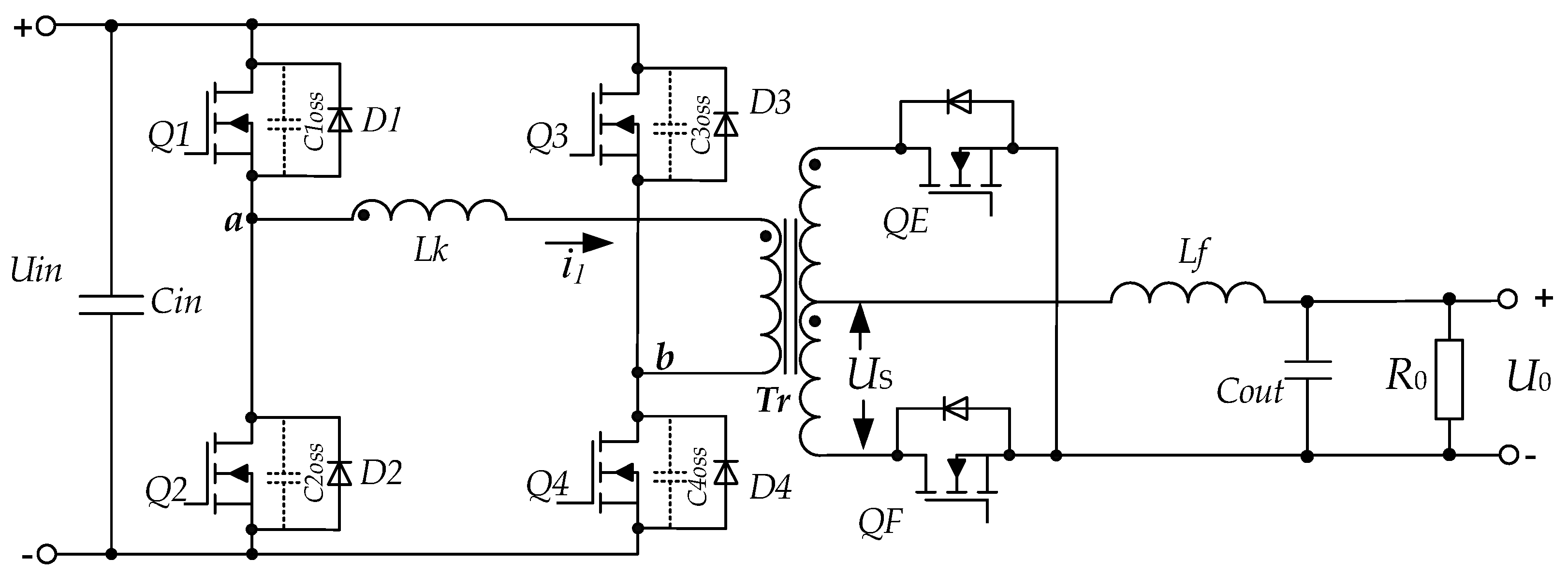
2. Electromagnetic Processes of the Phase-Shift Controlled Full-Bridge ZVS DC-DC Converter
The full-bridge phase-shift controlled zero-voltage-switched (ZVS) DC-DC converter with synchronous rectifier is shown in
Figure 1. The converter is composed of a bridge inverter (transistors
Q1 ÷
Q4 and their body diodes
D1 ÷
D4), an added commutating inductance
Lk, a matching transformer (
Tr) and a synchronous rectifier (transistors
QE,
QF). The output capacitances
C1oss ÷
C4oss of the transistors
Q1 ÷
Q4 are also shown with dashed lines. The left leg of the bridge (
Q1,
Q2) is denoted as “passive” and the right leg as “active” (
Q3,
Q4). The two arms of the bridge have completely different characteristics, which are essential when designing zero-voltage switching over a wide range of load change. The output filter elements are denoted by
Lf and
Cout, and the load by R
0. The waveforms explaining the operation of the circuit are illustrated in
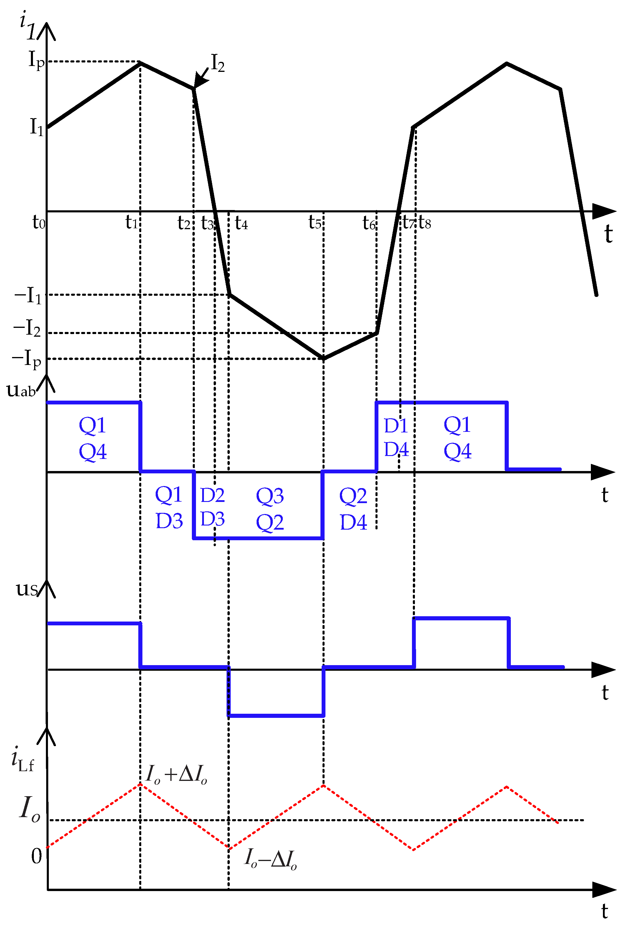
Figure 2.
To achieve zero-voltage turn-on, the stored energy in the commutating inductance Lk (including the leakage inductance of the transformer) is used to discharge the transistors’ output capacitance before they are turned on.
The electromagnetic processes of the phase-shift controlled full-bridge DC-DC converter operation can be divided into the following intervals [
1,
7,
8]:
t0 ÷ t1—during this interval transistors Q1, Q4, and QF are conducting. The input voltage Uin is applied to the primary side (uab). At time t1 Q4 turns off and the current in the primary side of the transformer charges capacitance C4oss and discharges capacitance C3oss, turning on body diode D3. Once diode D3 begins conduction, switch Q3 can be turned on under ZVS conditions.
t1 ÷ t2—the devices Q1 and D3 are conducting and the primary side voltage is clamped to zero. At time t2, Q1 turns off and the current in the primary side charges capacitance C1oss and discharges capacitance C2oss, turning on body diode D2.
t2 ÷ t3—the primary current i1 flows through body diodes D2 and D3 during the corresponding conduction interval. Transistor Q2 will be switched on at zero-voltage. The voltage across the secondary winding us continues clamped to zero (the secondary winding of the transformer is electrically shorted as transistors QE and QF are turned on).
t3 ÷ t4—during this interval, transistors Q2 and Q3 are turned on. The voltage across the secondary winding continues, clamped to zero.
t4 ÷ t5—transistors Q2, Q3, and QE are conducting. The input voltage (-Uin) is applied to the primary side uab. At time t5, Q3 turns off and the current in the primary side i1 charges capacitance C3oss and discharges capacitance C4oss, turning on body diode D4. Once diode D4 begins conduction, switch Q4 can be turned on under ZVS conditions.
t5 ÷ t6—the devices Q2 and D4 are conducting and the primary side voltage uab is clamped to zero. At time t6, Q2 turns off and the current in the primary side i1 charges capacitance C2oss and discharges capacitance C1oss, turning on body diode D1.
t6 ÷ t7—the primary current i1 flows through diodes D1 and D4 during this interval. Furthermore, transistor Q4 will be switched on at zero-voltage. The voltage across the secondary winding continues, clamped to zero (QE and QF are conducting).
After the time t7, transistors Q4 and Q1 are turned on, and in the following time intervals, the electromagnetic processes are repeated.
Zero-voltage switching (ZVS) for transistors
Q3 and
Q4 is possible even under light load conditions, as the energy stored in the output filter inductor is sufficient to activate diodes
D3 and
D4. In contrast, transistors
Q1 and
Q2 can only achieve ZVS when the load current exceeds a certain critical threshold, denoted as
, as follows [
1]:
The current
I2 through
Lk at time t
2 can be evaluated as
where
;
n1 is the number of transformer primary side turns and
is the number of transformer secondary side turns.
Ultimately, zero-voltage switching is achieved when the load current exceeds the critical threshold
, which can be stated as
When the load current reflected to the primary side is lower than the effective magnetizing current, the magnetizing inductance contributes to the ZVS process. Under light load conditions, the energy available to charge or discharge the output capacitances of switches
Q1 and
Q2 comes from the energy stored in both the leakage inductance and the magnetizing inductance of the transformer [
1].
The converter voltage gain
M is equal to
where
Ds denotes the duty cycle of the secondary-side voltage
uS.
The primary side duty cycle
D is given by [
1]
The parameter accounts for the duty cycle reduction caused by the finite rise and fall times of the primary current waveform (t2 ÷ t4 and t6 ÷ t8, etc.).
For the primary side, the duty cycle can be expressed as follows [
1]:
To meet design requirements for a specified output power, input-to-output voltage ratio, and maximum allowable duty cycle, the transformer turn ratio, switching frequency, and added commutating inductance must be appropriately selected to satisfy the necessary operating conditions.
3. Simulation and Experimental Results
To evaluate the presented results, a full-bridge phase-shift controlled ZVS converter was studied for the following input data: output power
P0 = 120 W; input voltage
Uin = 36 V ÷ 48 V (±1 V); output voltage
U0 = 12 V ± 1%; switching frequency
fS = 200 kHz. The commutating inductance
Lk = 300 nH. The LTC3722-1 phase-shift PWM controller was chosen and the MOSFET used was Si7852DP [
9,
10]. To meet the output current ripples, an output filter inductance
Lf = 2.4 μH was chosen. To meet the output voltage ripples, an output filter capacitance
Cout = 1000 μF was chosen. The simulations were performed at load current
I0 = 4 A, 8 A. The output inductor
Lf peak-to-peak ripple current was set to 20% ÷ 30% of the output current.
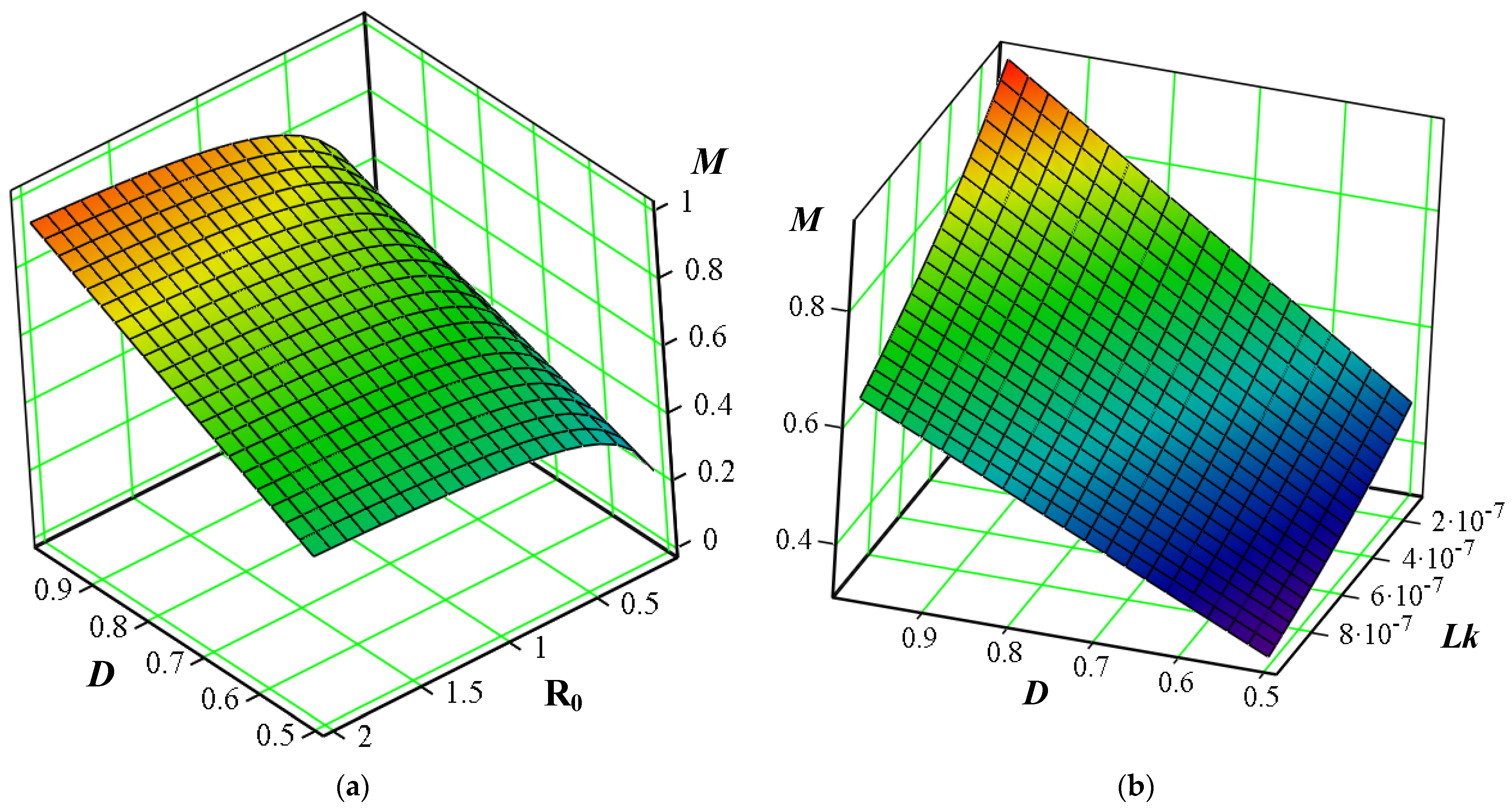
On the basis of the given input data, using (7), the dependencies
and
are plotted in
Figure 3.
It is shown that an increase in the added commutating inductance Lk can extend the range of load conditions under which ZVS occurs. However, due to the finite rise and fall times of the primary current, the effective duty cycle in the transformer’s secondary winding is reduced. This results in a decrease in the converter’s voltage gain. As a result, the voltage gain becomes dependent on the commutating inductance Lk (including transformer leakage inductance), switching frequency, and load conditions.
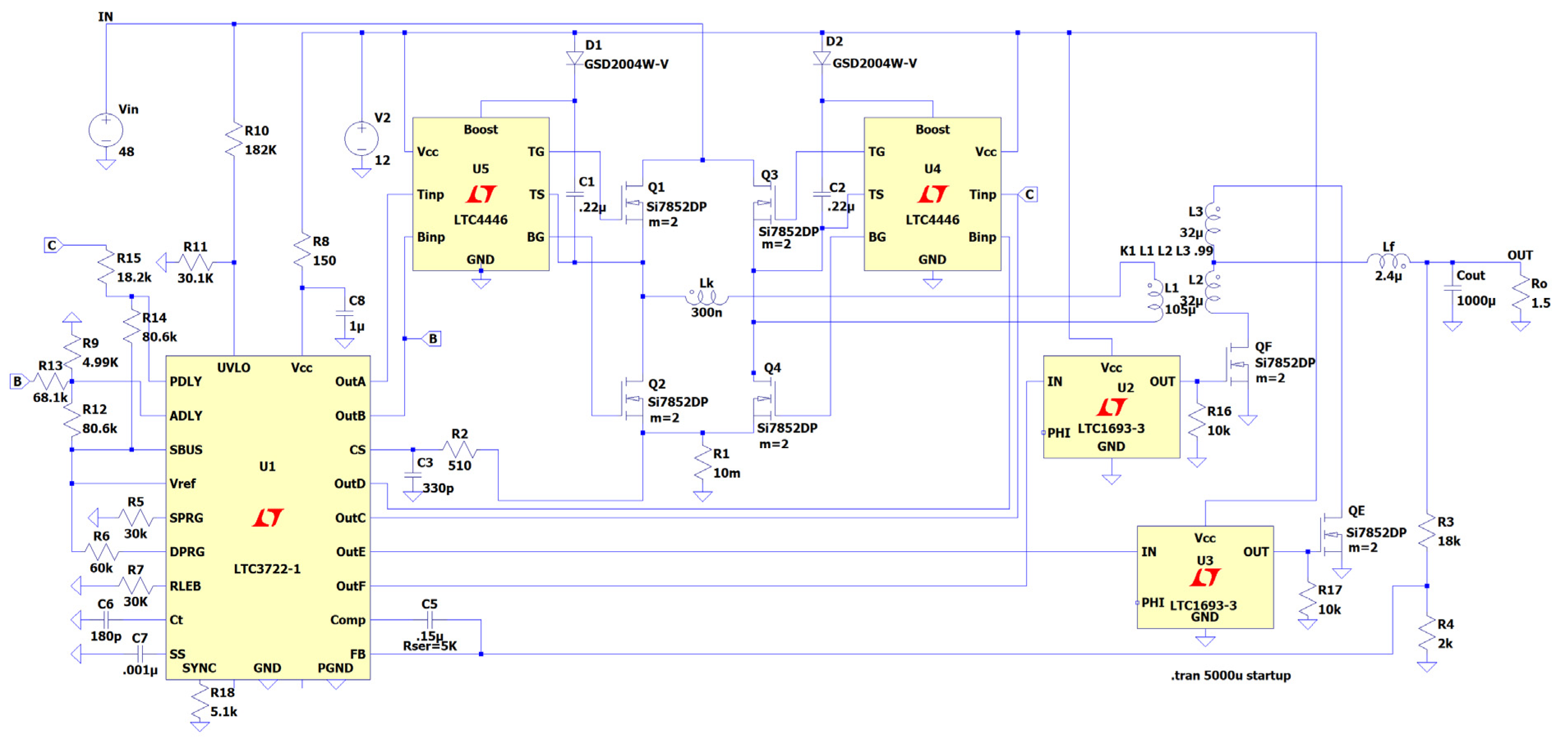
The LTSpice simulation circuit is shown in
Figure 4. The circuit is based on the approach given in [
9].
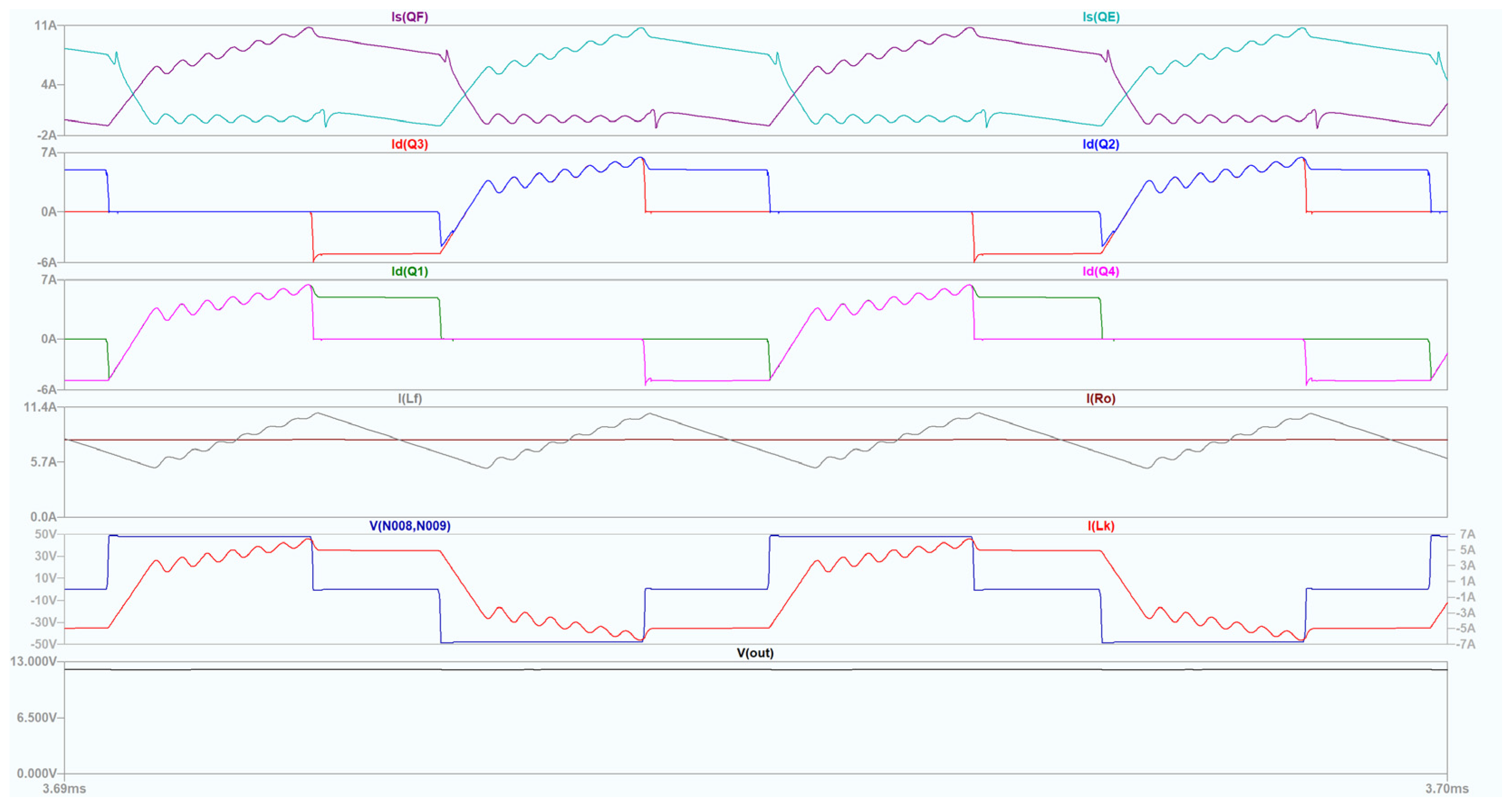
The simulation results for input voltage
Uin = 48 V, output voltage
U0 = 12 V, and output current
I0 = 8 A are presented in
Figure 5, as follows: from top to bottom: 1 plot plane—current trough transistors
QE (Is(QE) green) and
QF (Is(QF) dark red); 2 plot plane—current trough transistors
Q2 (Id(Q2) blue) and
Q3 (Id(Q3) red); 3 plot plane—current trough transistors
Q1 (Id(Q1) green) and
Q4 (Id(Q4) pink); 4 plot plane—current trough filter inductance
Lf (I(Lf) gray) and output current (I(Ro) brown); 5 plot plane—current trough
Lk (I(Lk) red) and voltage u
ab (V(N008,N009) dark blue); 6 plot plane—output voltage
Uo (V(out) black).
The simulation validates that the waveforms of transistors Q1 ÷ Q4 and QE and QF are consistent with the theoretically predicted responses.
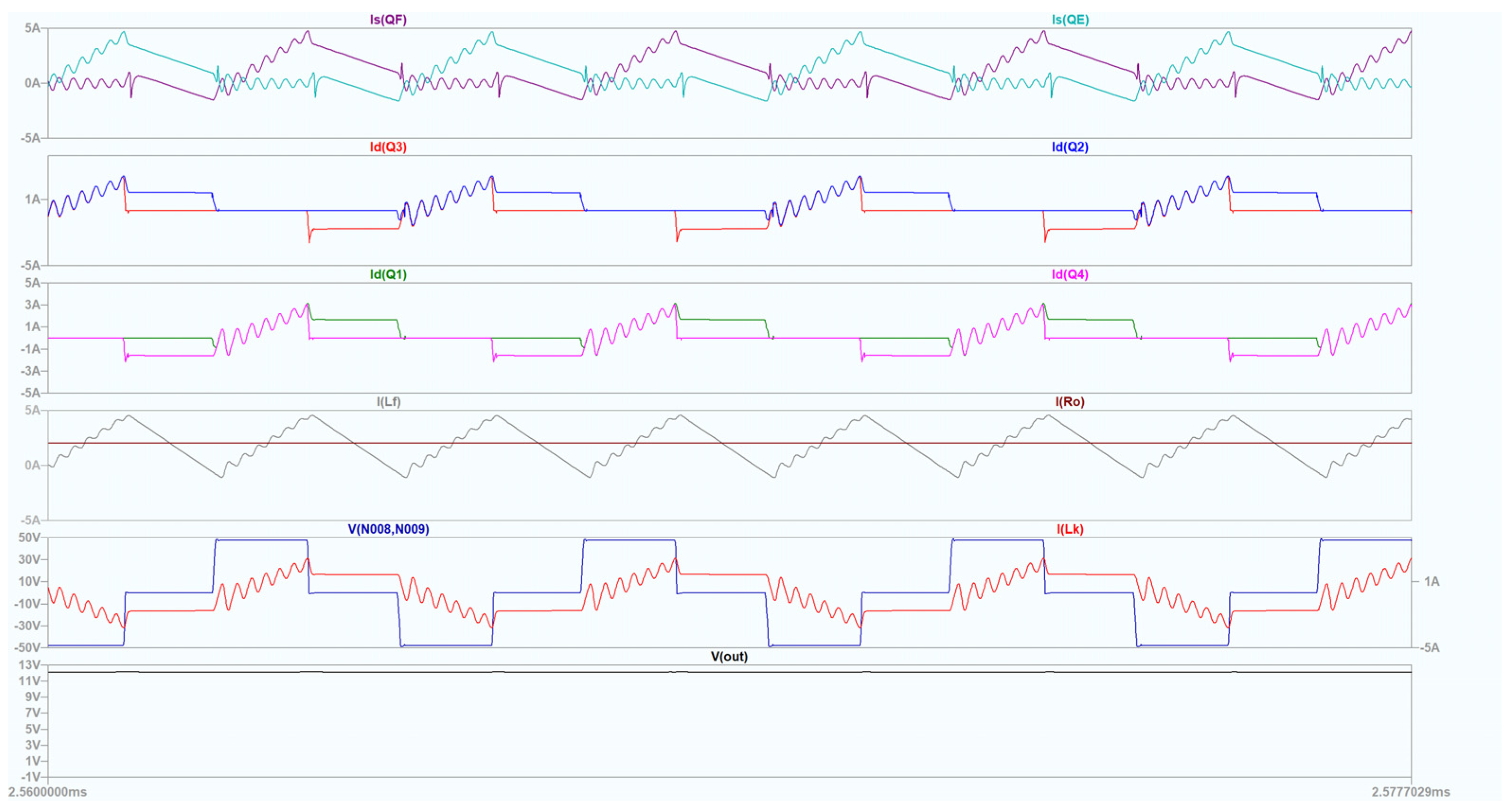
Using (1),
Icrit = 2.26 A has been calculated. Simulation with output current
Io = 2 A was performed. The results are proposed in
Figure 6.
The simulation results confirm that when the load current is smaller than , the ZVS conditions for transistors Q1 and Q2 are lost (from top to bottom: 2 plot plane—current trough transistor Q2 (Id(Q2) blue) and 3 plot plane—current trough transistor Q1 (Id(Q1) green).
Figure 7 and
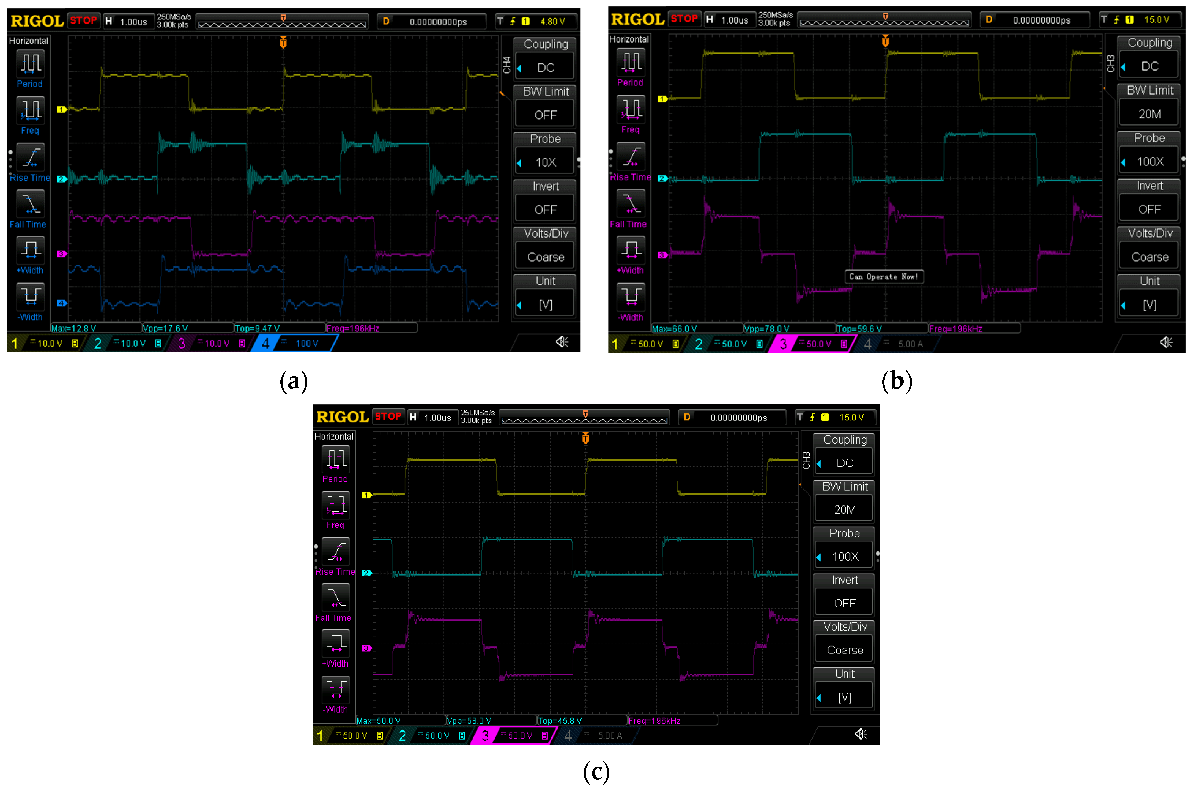
Figure 8 present the experimental data obtained using LTC3722-1 according to [
8,
9].
Figure 7 shows the experimental results for the input voltage 48 V/36 V and the output current 4 A: (a) from top to bottom input voltage 48 V: u
GSQ2, u
GSQ4, and u
GSQ3; (b) u
GSQ1 (yellow), u
GSQ3 (petroleum green), and output voltage u
0 (violet); (c) input voltage 36 V: u
GSQ1 (yellow), u
GSQ3 (petroleum green), and output voltage u
0 (violet).
Figure 8 shows the experimental results for the input voltage 48 V/36 V and the output current 8 A: (a) from top to bottom input voltage 48 V: u
GSQ2, u
GSQ4, u
GSQE, and u
GSQF; (b) u
GSQ1 (yellow), u
GSQ3 (petroleum green), and output voltage u
0 (violet); (c) input voltage 36 V: u
GSQ1 (yellow), u
GSQ3 (petroleum green), and output voltage u
0 (violet).
The experimental results validate that the waveforms of transistors Q1 ÷ Q4 and QE and QF are consistent with the theoretically predicted responses.
4. Conclusions
This paper presents a study of a phase-shift controlled ZVS full-bridge DC-DC converter employing synchronous rectification using the LTC3722 controller. A comprehensive analysis is proposed to investigate the influence of the added commutating inductance on ZVS conditions, the precision of switching control, and the dynamic interaction between ZVS performance and varying load conditions. On the basis of the conducted study, we can conclude that the effective duty cycle range is reduced, as greater leakage inductance is needed to achieve ZVS. Moreover, due to circulating current components, higher RMS currents in the bridge are achieved.
Furthermore, the phase-shift controlled full-bridge DC-DC converter exhibits the following advantages: operation with pulse-width modulation (PWM) at a constant switching frequency; the enablement of zero-voltage switching (ZVS) for the active switches, resulting in a significant reduction in switching stress, losses, and electromagnetic interference (EMI); and the use of the intrinsic body diodes of MOSFETs, eliminating the need for fast-recovery diodes.
The analytical results are verified by simulation with LTSpice and with experimental data. Therefore, the discussed methodology for the investigation of the influence of the added commutating inductance on ZVS conditions can find applications both in engineering practice and in the education of students in power electronics.


