Proceeding Paper

0.1 THz Imaging with a Monolithic High-Tc Superconducting Transition-Edge Detector †

1
Electrical Engineering Department, Sharif University of Technology, Tehran 11155, Iran
2
Faculty of Basic Sciences, Tarbiat Modares Unievrsity, Tehran 14115, Iran
*
Author to whom correspondence should be addressed.
Presented at the 8th International Electronic Conference on Sensors and Applications, 1–15 November 2021; Available online: https://ecsa-8.sciforum.net/.
Eng. Proc. 2021, 10(1), 71; https://doi.org/10.3390/ecsa-8-11304
Published: 1 November 2021

Abstract

:
Terahertz imaging has attracted significant interest for its applications in noninvasive medical diagnosis, security systems, and industrial inspections. Superconducting bolometers are one of the promising technologies of ultra-sensitive terahertz detection. Here, we present THz images captured by a low-cost superconducting transition-edge detector. The sensing element of the detector is a meander line patterned YBa 2 Cu 3 O 7 x (YBCO) thin film realizing monolithically the absorber and thermometer of the detector. A total of 400 nm YBCO film is deposited on Yttrium-stabilized Zirconia substrate by the metal-organic deposition method which is well-known as an economic and scalable chemical, vacuum-free technique. The meander line pattern consists of 15 series connected parallel lines with a length of 1.5 mm and a width of 50 micrometers. This pattern has shown a significant response to the 0.1 THz equivalents to 3 mm wavelength radiation without any coupled antenna or separate absorber that may reduce the detection speed. The voltage response amplitude of the fabricated detector to 0.1 THz radiation at different modulation frequencies is measured and the detector is utilized for imaging concealed objects including cigarettes and metallic items.

1. Introduction

During recent years, terahertz (THz) technology has shown a great potential for a wide range of applications from basic sciences to industry [1,2,3,4,5,6]. Unique properties of THz radiation including (i) low photon energy, (ii) high transmission through most of the dielectrics, and (iii) reflection from metals make it an excellent candidate for many imaging applications especially medical and security imaging [7,8,9,10,11,12]. Despite many applications and interest in THz technology, this part of the electromagnetic radiation spectrum has not been thoroughly explored until twenty years ago because of the lack of high-performance and compact THz sources and detectors.
Superconducting materials have attracted much attention as an advantageous choice for both source and detector from the early stages of developing THz technology [13,14]. Continues wave THz emission from the stack of intrinsic Josephson junctions formed in a single crystal high- T c superconductor Bi 2 Sr 2 CaCu 2 O 8 + δ (Bi2212) was first reported in 2007 [15]. Afterward, some other groups focused on improving the performance of these kinds of THz radiation sources [16,17,18,19,20,21]. On the other hand, the first superconducting detector for sub-millimeter-wave radiation was proposed in the early 1960s [22]. This superconductor tunnel junction (STJ) is categorized as a pair breaking detector. Other structures with a similar mechanism such as superconductor-insulator-superconductor (SIS) and superconductor-insulator-normal metal (SIN) detectors were proposed in the following years [23,24]. Another group of superconducting detectors are hot-electron bolometers (HEBs) and transition-edge bolometers (TEBs) that are quite similar in fundamental mechanism [25]. Superconducting TEBs work based on small temperature change caused by absorption of incident radiation. TEB should be biased at the middle of the normal-superconductor transition, so the small temperature variation will cause a considerable resistance variation that can be measured as a voltage or current signal. One of the challenges for using superconducting bolometers as a THz detector is coupling the mm-wave radiation to the sensing element. The standard approaches for implementing this coupling are by using either an absorbing layer or coupling an antenna to the sensor. Detectors that employ separate absorber are called composite bolometer. Incident radiation should be captured by the absorbing material so the absorber sheet resistant must be equal to the free-space impedance and its area should be on the order of λ 2 where λ is the wavelength of the incoming radiation. Detectors that have a sensing element acting as an absorber are called monolithic bolometer. These bolometers are usually practical for infrared wavelengths and antenna-coupled microbolometers are proposed for the THz waves.
In this article, we demonstrate THz images captured by a monolithic superconducting TEB fabricated by an economic method. Response of the fabricated bolometer to the 0.1 THz radiation versus temperature at different modulation frequencies and THz images of concealed cigarettes and metallic objects taken by this detector are presented.

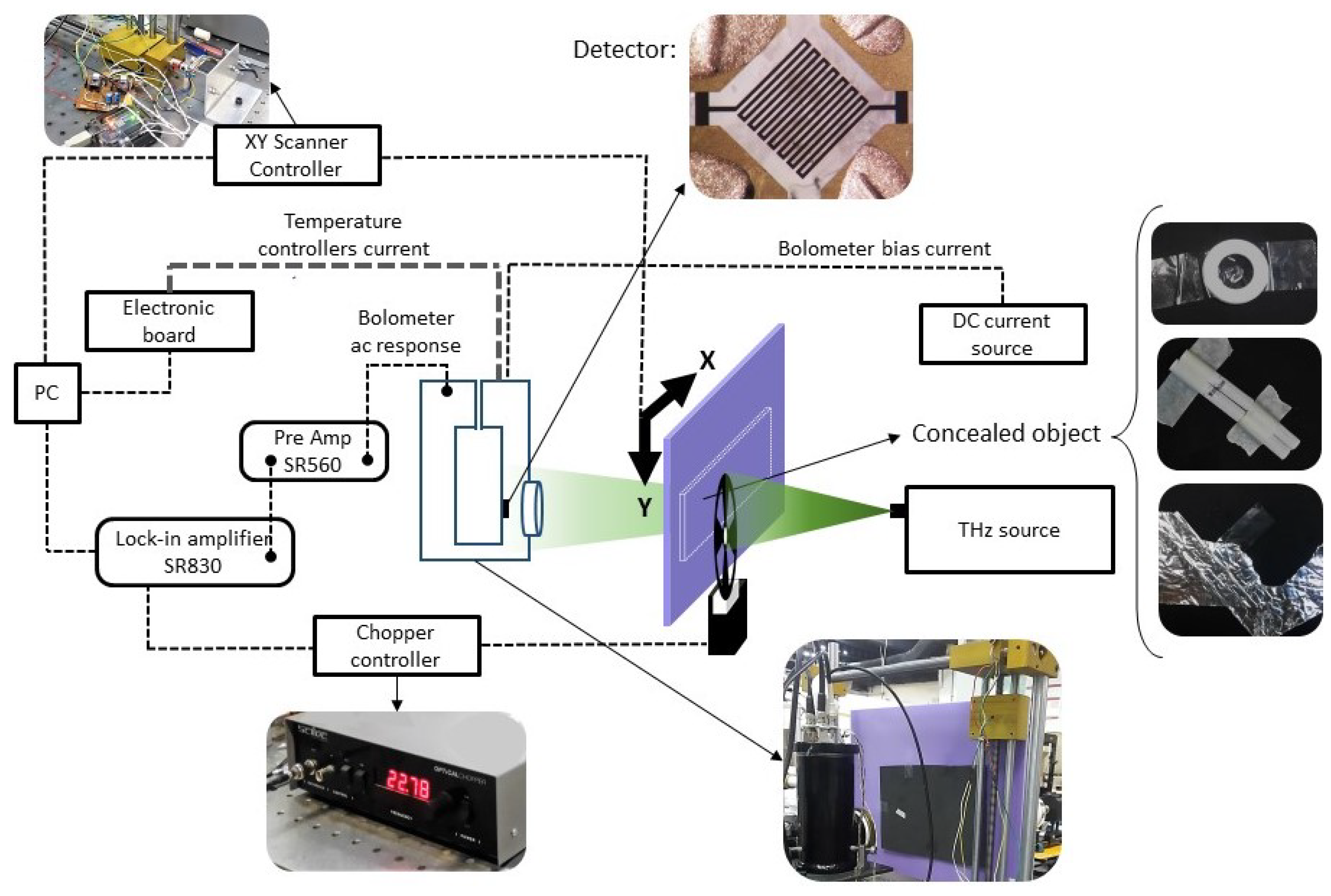
2. Materials and Methods

2.1. THz Detector

The THz detector used in this work is a superconducting TEB composed of 400 nm YBCO thin film deposited on a 500 μ m thick Yttrium-stabilized Zirconia (YSZ) substrate by the metal-organic deposition (MOD) method [26,27]. A Ce 0.9 La 0.1 O 2 (CLO) buffer layer is required to compensate the lattice mismatch between YBCO and YSZ substrate and to achieve a high-quality YBCO thin film. Therefore, a 20 nm CLO buffer layer is deposited by the same MOD method. Then, the bolometer pattern is fabricated by the standard optical lithography on the YBCO thin film. The designed pattern is a meander line shape consisting of 15 lines that are 1.5 mm long and 50 μ m wide with 4 contact pads.

2.2. Imaging Setup

The fabricated detector is placed inside a liquid nitrogen cryostat designed for optical characterization. The bias temperature of the detector is adjusted by two PT100 sensors and a heater, all controlled by a computer interface. The detector is electrically biased by a low noise DC current source in a four-probe configuration. The 0.1 THz response of the bolometer is measured for different modulation frequencies. The mm-wave source we have used here is a TeraSense 100 GHz source with a maximum output power of 70 mW. For high precision data collection, a lock-in amplifier in combination with a low-noise pre-amplifier is used to record the voltage response in the same modulation frequency that the mm-wave source is modulated by a mechanical chopper. A schematic of the imaging setup including the microscopic image of the detector is shown in Figure 1. According to Figure 1, an XY-scanner is used for scanning the concealed objects in front of the detector for recording the THz image. The XY-scanner controller is synchronized with the data acquisition program to reconstruct the image from the voltage response measured for each pixel.

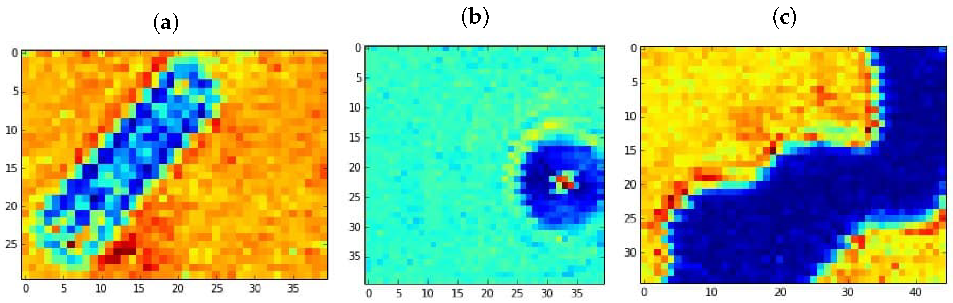
3. Results and Discussion

The measured resistance versus temperature of the detector shows a sharp normal-superconductor transition indicating high quality YBCO film. The voltage response of the fabricated TEB is measured versus temperature at three different modulation frequencies that are shown in Figure 2. According to Figure 2, it can be observed that the maximum voltage response of the detector appears at the middle of the transition width, where the sensitivity of the resistance to temperature has the maximum value. In addition, the amplitude of the response decreases by increasing the modulation frequency that can not be avoided in a thermal detector. The behavior of the voltage amplitude and phase response versus modulation frequencies for these kind of bolometers were previously discussed in detail in [28].
The bolometer design used in this paper does not need any coupled antenna owing to the fact that the superconducting YBCO meander lines act as a lossy antenna and absorb part of energy. In addition, YSZ substrate also contributes in the absorption of the incoming mm-wave power, while the substrate thermal properties increases the voltage response of the bolometer [27]. Here, we have used a single-pixel TEB for imaging hidden objects in front of a 0.1 THz source modulated at 22 Hz in transmission configuration. The first objects used for imaging are two cigarettes concealed between two polystyrene boards. The 0.1 THz image of the cigarettes is shown in Figure 3a. The spatial resolution of this image is adjusted to be 30 × 40 pixels. Tobacco absorbes terahertz radiation [29] causing a contrast in the captured image. The next objects are a metallic flat washer (Figure 3b) and an arbitrarily shaped aluminum foil (Figure 3c) placed between two polystyrene boards. Resolution of this images is 40 × 40 pixels and 35 × 45 pixels, respectively. Because of the high reflectivity of metals in the terahertz range, there will be a huge contrast in the captured image. THz images of these three objects shown in Figure 3 are indicated without any post-processing. The voltage response amplitude of the bolometer could be increased by using a thinner substrate and optimizing the bolometer pattern. Increasing the current bias would also increase the response amplitude but we are limited by the thermal runaway phenomena [30]. Increasing the voltage response enables us to increase the modulation frequency and achieve higher resolution images in a short time. The fabrication process of the device is also affordable to make arrays of bolometers for fast and high resolution imaging.

4. Conclusions

The 0.1 THz images of concealed objects have been captured by the fabricated monolithic transition-edge bolometer. The YBCO thin film used in this work is grown by the metal-organic deposition method that is a cost-effective and scalable technique. Maximum response of the bolometer is obtained at 88.5 K and THz imaging is carried out at this temperature. The imaging is performed in transmission mode while the incoming radiation is modulated at 22 Hz. Design and fabrication process of the detector used in this work has the potential of fabricating large area arrays to improve the resolution of the image and imaging speed.

Author Contributions

Conceptualization, R.N. and M.F.; Writing—Original Draft Preparation, R.N.; Writing—Review and Editing, R.N., R.M. and M.F.; Device fabrication, R.M.; Data Curation, R.N. and S.I.M.; Investigation, all authors; Supervision, M.F. All authors have read and agreed to the published version of the manuscript.

Funding

This research received no external funding.

Conflicts of Interest

The authors declare no conflict of interest.

References

  1. Park, H.; Son, J.H. Machine Learning Techniques for THz Imaging and Time-Domain Spectroscopy. Sensors 2021, 21, 1186. [Google Scholar] [CrossRef] [PubMed]
  2. Di Fabrizio, M.; D’Arco, A.; Mou, S.; Palumbo, L.; Petrarca, M.; Lupi, S. Performance evaluation of a THz pulsed imaging system: Point spread function, broadband THz beam visualization and image reconstruction. Appl. Sci. 2021, 11, 562. [Google Scholar] [CrossRef]
  3. Zhang, J.Y.; Ren, J.J.; Li, L.J.; Gu, J.; Zhang, D.D. THz imaging technique for nondestructive analysis of debonding defects in ceramic matrix composites based on multiple echoes and feature fusion. Opt. Express 2020, 28, 19901–19915. [Google Scholar] [CrossRef] [PubMed]
  4. Yang, Z.; Tang, D.; Hu, J.; Tang, M.; Zhang, M.; Cui, H.L.; Wang, L.; Chang, C.; Fan, C.; Li, J.; et al. Near-Field Nanoscopic Terahertz Imaging of Single Proteins. Small 2021, 17, 2005814. [Google Scholar] [CrossRef]
  5. Lane, P.; Cunningham, P.; Melinger, J.; Esenturk, O.; Heilweil, E. Hot photocarrier dynamics in organic solar cells. Nat. Commun. 2015, 6, 1–6. [Google Scholar] [CrossRef] [PubMed] [Green Version]
  6. Ulbricht, R.; Hendry, E.; Shan, J.; Heinz, T.F.; Bonn, M. Carrier dynamics in semiconductors studied with time-resolved terahertz spectroscopy. Rev. Mod. Phys. 2011, 83, 543. [Google Scholar] [CrossRef] [Green Version]
  7. Stantchev, R.I.; Yu, X.; Blu, T.; Pickwell-MacPherson, E. Real-time terahertz imaging with a single-pixel detector. Nat. Commun. 2020, 11, 1–8. [Google Scholar] [CrossRef] [PubMed]
  8. Appleby, R.; Anderton, R.N. Millimeter-wave and submillimeter-wave imaging for security and surveillance. Proc. IEEE 2007, 95, 1683–1690. [Google Scholar] [CrossRef]
  9. Yeom, S.; Lee, D.S.; Son, J.Y.; Jung, M.K.; Jang, Y.; Jung, S.W.; Lee, S.J. Real-time outdoor concealed-object detection with passive millimeter wave imaging. Opt. Express 2011, 19, 2530–2536. [Google Scholar] [CrossRef] [PubMed]
  10. Zhang, Y.; Wang, C.; Huai, B.; Wang, S.; Zhang, Y.; Wang, D.; Rong, L.; Zheng, Y. Continuous-Wave THz Imaging for Biomedical Samples. Appl. Sci. 2021, 11, 71. [Google Scholar] [CrossRef]
  11. D’Arco, A.; Di Fabrizio, M.; Dolci, V.; Petrarca, M.; Lupi, S. THz pulsed imaging in biomedical applications. Condens. Matter 2020, 5, 25. [Google Scholar] [CrossRef] [Green Version]
  12. Lindley-Hatcher, H.; Stantchev, R.; Chen, X.; Hernandez-Serrano, A.; Hardwicke, J.; Pickwell-MacPherson, E. Real time THz imaging—Opportunities and challenges for skin cancer detection. Appl. Phys. Lett. 2021, 118, 230501. [Google Scholar] [CrossRef]
  13. Kreisler, A.J.; Gaugue, A. Recent progress in high-temperature superconductor bolometric detectors: From the mid-infrared to the far-infrared (THz) range. Supercond. Sci. Technol. 2000, 13, 1235. [Google Scholar] [CrossRef]
  14. Demirhan, Y.; Turkoglu, F.; Altan, H.; Sabah, C.; Ozyuzer, L. THz Sources and Detectors Fabricated from High Temperature Superconductors. In Terahertz (THz), Mid Infrared (MIR) and Near Infrared (NIR) Technologies for Protection of Critical Infrastructures Against Explosives and CBRN; Springer: Dordrecht, The Netherlands, 2021; pp. 153–164. [Google Scholar]
  15. Ozyuzer, L.; Koshelev, A.E.; Kurter, C.; Gopalsami, N.; Li, Q.; Tachiki, M.; Kadowaki, K.; Yamamoto, T.; Minami, H.; Yamaguchi, H.; et al. Emission of coherent THz radiation from superconductors. Science 2007, 318, 1291–1293. [Google Scholar] [CrossRef] [PubMed] [Green Version]
  16. Tsujimoto, M.; Yamaki, K.; Deguchi, K.; Yamamoto, T.; Kashiwagi, T.; Minami, H.; Tachiki, M.; Kadowaki, K.; Klemm, R.A. Geometrical resonance conditions for THz radiation from the intrinsic Josephson junctions in Bi2Sr2CaCu2O8+ δ. Phys. Rev. Lett. 2010, 105, 037005. [Google Scholar] [CrossRef] [PubMed] [Green Version]
  17. Wang, H.; Guénon, S.; Gross, B.; Yuan, J.; Jiang, Z.; Zhong, Y.; Grünzweig, M.; Iishi, A.; Wu, P.; Hatano, T.; et al. Coherent terahertz emission of intrinsic Josephson junction stacks in the hot spot regime. Phys. Rev. Lett. 2010, 105, 057002. [Google Scholar] [CrossRef] [Green Version]
  18. Welp, U.; Kadowaki, K.; Kleiner, R. Superconducting emitters of THz radiation. Nat. Photonics 2013, 7, 702–710. [Google Scholar] [CrossRef]
  19. Klemm, R.A.; Delfanazari, K.; Tsujimoto, M.; Kashiwagi, T.; Kitamura, T.; Yamamoto, T.; Sawamura, M.; Ishida, K.; Hattori, T.; Kadowaki, K. Modeling the electromagnetic cavity mode contributions to the THz emission from triangular Bi2Sr2CaCu2O8+ δ mesas. Phys. C Supercond. 2013, 491, 30–34. [Google Scholar] [CrossRef] [Green Version]
  20. Kashiwagi, T.; Yamamoto, T.; Minami, H.; Tsujimoto, M.; Yoshizaki, R.; Delfanazari, K.; Kitamura, T.; Watanabe, C.; Nakade, K.; Yasui, T.; et al. Efficient fabrication of intrinsic-Josephson-junction terahertz oscillators with greatly reduced self-heating effects. Phys. Rev. Appl. 2015, 4, 054018. [Google Scholar] [CrossRef]
  21. Ono, Y.; Minami, H.; Kuwano, G.; Kashiwagi, T.; Tsujimoto, M.; Kadowaki, K.; Klemm, R. Superconducting emitter powered at 1.5 terahertz by an external resonator. Phys. Rev. Appl. 2020, 13, 064026. [Google Scholar] [CrossRef]
  22. Burstein, E.; Langenberg, D.; Taylor, B. Superconductors as quantum detectors for microwave and sub-millimeter-wave radiation. Phys. Rev. Lett. 1961, 6, 92. [Google Scholar] [CrossRef]
  23. Dolan, G.; Phillips, T.; Woody, D. Low-noise 115-GHz mixing in superconducting oxide-barrier tunnel junctions. Appl. Phys. Lett. 1979, 34, 347–349. [Google Scholar] [CrossRef]
  24. Ariyoshi, S.; Otani, C.; Dobroiu, A.; Sato, H.; Kawase, K.; Shimizu, H.; Taino, T.; Matsuo, H. Terahertz imaging with a direct detector based on superconducting tunnel junctions. Appl. Phys. Lett. 2006, 88, 203503. [Google Scholar] [CrossRef]
  25. Kraus, H. Superconductive bolometers and calorimeters. Supercond. Sci. Technol. 1996, 9, 827. [Google Scholar] [CrossRef]
  26. Zhao, Y.; Wu, W.; Tang, X.; Andersen, N.H.; Han, Z.; Grivel, J.C. Epitaxial growth of YBa2Cu3O7-x films on Ce0.9La0.1O2-y buffered yttria-stabilized zirconia substrates by an all-chemical-solution route. CrystEngComm 2014, 16, 4369–4372. [Google Scholar] [CrossRef]
  27. Mohajeri, R.; Opata, Y.A.; Wulff, A.C.; Grivel, J.C.; Fardmanesh, M. All Metal Organic Deposited High-T c Superconducting Transition Edge Bolometer on Yttria-Stabilized Zirconia Substrate. J. Supercond. Nov. Magn. 2017, 30, 1981–1986. [Google Scholar] [CrossRef]
  28. Nazifi, R.; Mohajeri, R.; Alipour, Z.; Mirzaei, S.I.; Ahmadi-Boroujeni, M.; Vesaghi, M.; Grivel, J.C.; Fardmanesh, M. Millimeter-Wave Response of All Metal-Organic Deposited YBCO Transition Edge Bolometer. IEEE Trans. Appl. Supercond. 2020, 31, 1–5. [Google Scholar] [CrossRef]
  29. Chan, W.L.; Deibel, J.; Mittleman, D.M. Imaging with terahertz radiation. Rep. Prog. Phys. 2007, 70, 1325. [Google Scholar] [CrossRef]
  30. Fardmanesh, M.; Rothwarf, A.; Scoles, K.J. Low and midrange modulation frequency response for YBCO infrared detectors: Interface effects on the amplitude and phase. IEEE Trans. Appl. Supercond. 1995, 5, 7–13. [Google Scholar] [CrossRef]
Figure 1. Schematic of the imaging setup.
Engproc 10 00071 g001
Figure 2. Amplitude of the measured response of the bolometer at three different modulation frequencies versus bias temperature. The inset shows the measured resistance versus temperature. In all measurements the device is current biased by 500 μ A.
Engproc 10 00071 g002
Figure 3. THz images of concealed (a) cigarettes, (b) metallic flat washer, and (c) arbitrary shape aluminum foil captured in transmission mode.
Engproc 10 00071 g003
Publisher’s Note: MDPI stays neutral with regard to jurisdictional claims in published maps and institutional affiliations.

