1. Introduction
The rapid growth in global energy demand, together with the environmental challenges associated with fossil fuel consumption, has accelerated the transition toward sustainable energy solutions [
1]. Various energy harvesting approaches have emerged, enabling the utilization of renewable resources such as solar radiation, wind, geothermal heat, and ambient mechanical vibrations. The application of such technologies to existing infrastructure allows for transforming environmental energy into usable electricity and enhancing energy efficiency and the shift to decentralized, low-emission energy systems [
2]. Consequently, multi-source hybrid energy systems have been viewed as flexible and green ways of designing the current power grids.
Among renewable energy sources, solar energy stands out due to its abundance and widespread availability across most regions of the world. Both photovoltaic and solar thermal technologies provide efficient means of converting solar energy into electricity and heat, contributing significantly to the reduction in greenhouse gas emissions. As global electricity demand continues to rise, the large-scale deployment of solar energy systems has become essential for countries aiming to establish sustainable and resilient energy infrastructures [
3,
4].
Perovskite solar cells are a technologically developing form of photovoltaic cell that has gained significant interest over the past few years. They are attractive due to their capabilities in attaining high power conversion efficiencies and relatively low fabrication costs relative to conventional silicon-based solar cells [
5]. These materials exhibit strong light absorption, adjustable bandgap properties, and can be processed into thin films using low-temperature and cost-effective techniques. Such characteristics make them promising candidates for next-generation solar energy applications. However, their survival in the long run is still a significant problem that curtails their commercialization. Moisture exposure, thermal fluctuations, oxygen interaction, and ultraviolet radiation are some of the causes of the gradual degradation of the perovskite structure, which adversely impact the device performance. To resolve these problems, material engineering, better methods of encapsulation, and interface engineering have to be improved to increase device longevity [
6,
7].
The structural, morphological, and phase properties of photovoltaic materials are highly sensitive to temperature variations. Temperature variations have the ability to cause phase changes, alter the behaviour of grain boundaries, and form defect states, all of which affect the charge transport mechanisms and electrical conductivity. These effects also impact energy band alignment across different layers, ultimately affecting charge collection efficiency and overall device performance [
8,
9]. Conventional characterization techniques typically rely on current–voltage (J–V) measurements to extract key parameters such as open-circuit voltage (Voc), short-circuit current density (Jsc), fill factor (FF), and power conversion efficiency (PCE). Besides these techniques, impedance spectroscopy (IS) can give more insight into what is happening inside the device by separating the contributions of charge transport, recombination, diffusion, and resistive components of the electrodes and interfaces [
10,
11].
Temperature-dependent investigations are essential for understanding the operational reliability and long-term stability of perovskite solar cells because the electrical properties of these materials are highly sensitive to thermal variations. Temperature directly influences carrier mobility, defect-assisted recombination, energy-band alignment, and interface charge transfer, thereby affecting both photovoltaic performance and impedance response. Although numerous studies have examined the influence of temperature on photovoltaic parameters, relatively few have combined current–voltage characterization with impedance spectroscopy to establish a direct relationship between macroscopic device performance and the underlying electrical transport mechanisms in lead-free perovskite solar cells [
11,
12,
13].
The present study focuses on a quantitative investigation of the electrical and impedance characteristics of perovskite solar cells with the structure FTO/ETL (C60, PCBM, SnS
2, ZnSe)/CH
3NH
3SnBr
3/Cu
2O using the SCAPS-1D simulation tool [
14]. This approach enables a detailed analysis of charge-transport phenomena within the device and provides a basis for understanding the temperature-dependent behavior of the investigated solar cells. In particular, the study examines the evolution of the photovoltaic response and impedance characteristics with temperature, with emphasis on the electrical processes responsible for the observed changes in device performance.
It should be emphasized that the photovoltaic parameters obtained from the SCAPS-1D J–V simulations are based on the device architecture and material parameters previously reported [
14]. Therefore, the J–V results presented in this study are not intended to constitute a new prediction or optimization of the photovoltaic architecture itself. Rather, the main contribution of the present work is the systematic investigation of the temperature-dependent impedance response of this device using complementary Nyquist, Bode, electric-modulus, and equivalent-circuit analyses. This combined approach enables the temperature-induced evolution of the effective recombination resistance, characteristic relaxation times, and frequency-dependent electrical processes to be identified and correlated with the corresponding photovoltaic response. In this way, the study provides deeper insight into the underlying electrical mechanisms governing the temperature dependence of the investigated lead-free perovskite solar cell.
2. Methodology and Device Architecture
The SCAPS-1D version 3.3.12 tool was applied to model heterojunction solar cells and study CH
3NH
3SnBr
3 as a PV material. The modeled device is made up of the following components: FTO (front contact), ETL (C
60, PCBM, SnS
2, or ZnSe), CH
3NH
3SnBr
3 (absorber), and Cu
2O (rear contact). The values of input parameters (such as bandgap energy, electron affinity, relative permittivity, and absorbance coefficient) were obtained using experimental/theoretical literature reports to guarantee physical consistency [
15].
Table 1 shows the most important parameters used in the simulation.
SCAPS-1D was selected because it is a well-established numerical simulator specifically developed for thin-film photovoltaic devices. It solves Poisson’s equation simultaneously with the electron and hole continuity equations under the drift–diffusion formalism, enabling accurate prediction of carrier transport, recombination, and photovoltaic performance. In addition to conventional current–voltage calculations, SCAPS-1D provides AC analysis capabilities that allow impedance spectroscopy simulations over a broad frequency range. These features make SCAPS-1D particularly suitable for investigating the influence of temperature on both the photovoltaic characteristics and the equivalent electrical response of lead-free perovskite solar cells while maintaining physically consistent material parameters and boundary conditions [
16].
Device functionality was simulated based on the solution of Poisson’s and the continuity equations for electrons and holes in steady state under illumination with AM 1.5G solar radiation (100 mW/cm2) at 300 K as follows:
Poisson’s equation
electron continuity equation
hole continuity equation
where ψ(x) represents the electrostatic potential, ε(x) the dielectric constant, G(x) the generation rate, and R(x) the total recombination rate, which includes Shockley–Read–Hall, radiative, and Auger recombination rates. The electron and hole current densities can be expressed as follows:
The solutions to the above-mentioned equations provided us with results in the form of J–V characteristics, EQE, and electrical potential distribution. Defect states in the absorber layer were modeled with a Gaussian energy distribution centered near the middle of the bandgap to describe bulk trap states that primarily contribute to Shockley–Read–Hall (SRH) recombination. The total defect density was fixed at Nt = 1 × 10
14 cm
−3, which lies within the range commonly reported for numerically optimized lead-free perovskite absorbers and provides a reasonable compromise between idealized and experimentally achievable material quality. Electron and hole capture cross-sections were both set to σn = σp = 1 × 10
−15 cm
2, following values widely adopted in the SCAPS literature for chalcogenide and perovskite absorbers. Assuming identical capture cross-sections for electrons and holes reduces the number of adjustable parameters and enables the influence of temperature to be evaluated without introducing additional asymmetry in the recombination kinetics [
17,
18].
SCAPS-1D enables simulating devices that consist of up to seven sequential layers; this feature makes it possible to specify the following characteristics for each of the layers: bandgap energy, electron affinity, dielectric constant, mobility, and defect concentration [
19,
20]. Additionally, it allows setting the necessary boundary conditions and contact parameters. Both DC and AC analyses are available in the program. As a result of the DC analysis, we receive the data required to calculate the following device characteristics:
where V
mp and
Jmp are the voltage and current density at the maximum power point, while Pin is the incident solar power. The AC approach produces impedance spectra covering a wide frequency range, allowing the study of charge transport, recombination, and interface-related phenomena at different biases, temperatures, and light levels [
21,
22].
It should be noted that the SCAPS-1D simulations performed in this work are based on a one-dimensional drift-diffusion formalism that solves Poisson’s equation together with the electron and hole continuity equations under steady-state conditions. Consequently, the model explicitly accounts for electronic charge transport, recombination, and defect-assisted processes through user-defined parameters. However, SCAPS does not explicitly incorporate microscopic ion migration, dynamic defect redistribution, phase transitions, structural degradation, or thermomechanical degradation mechanisms. Therefore, the simulated temperature-dependent trends should be interpreted as the consequences of changes in the electrical parameters implemented in the model rather than as direct evidence of atomistic or physicochemical degradation processes. These limitations should be considered when comparing the present simulations with experimental impedance measurements of perovskite solar cells [
23].
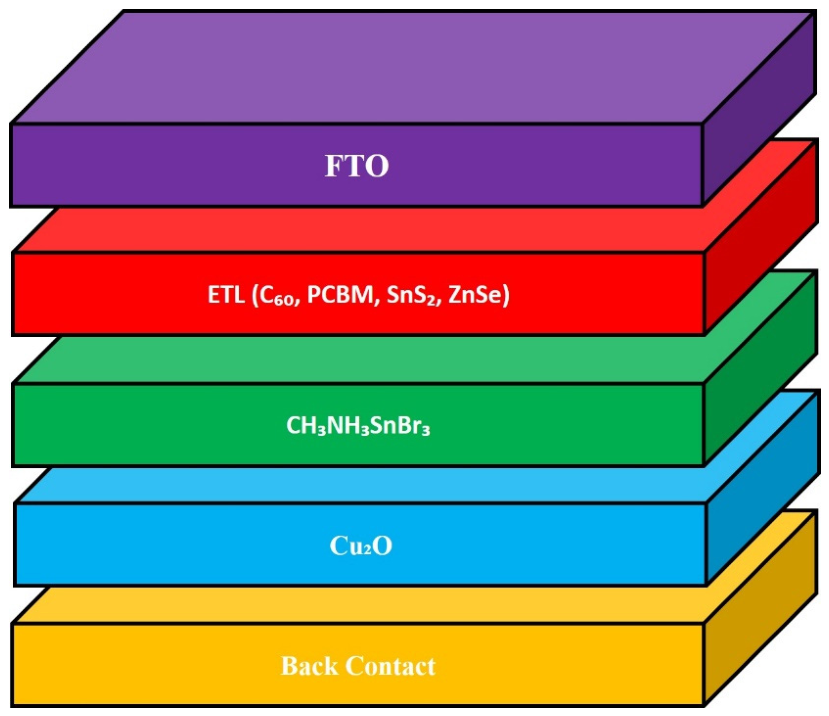
The device structure considered for the temperature-dependent simulations presented in this work is FTO/ZnSe/CH
3NH
3SnBr
3/Cu
2O (
Figure 1), where ZnSe serves as the electron transport layer (ETL). C
60, PCBM, and SnS
2 are included in
Table 1 as previously reported alternative ETL materials, but they are not comparatively investigated in the present temperature-dependent analysis. FTO is used as the transparent front electrode, while CH
3NH
3SnBr
3 serves as the lead-free absorber layer and Cu
2O as the hole transport layer (HTL).
The material parameters required for the SCAPS-1D simulations were adopted from previously reported literature data [
14] and were used as fixed input parameters rather than as variables for optimization, as summarized in
Table 1. Only the parameters directly relevant to the investigated FTO/ETL (C
60, PCBM, SnS
2, ZnSe)/CH
3NH
3SnBr
3/Cu
2O architecture are included in this manuscript. To improve clarity and avoid unnecessary duplication, the material properties have been reorganized and presented in a simplified form specifically for the present temperature-dependent impedance study.
Table 1.
Summary of the electrical parameters associated with each layer of the device [
14].
Table 1.
Summary of the electrical parameters associated with each layer of the device [
14].
| Material Property | FTO | C60 | PCBM | SnS2 | ZnSe | CH3NH3SnBr3 | Cu2O |
|---|
| Thickness (nm) | 0.02 | 20 | 20 | 150 | 20 | 700 | 0.05 |
| Bandgap, Eg (eV) | 3.5 | 1.7 | 2.0 | 1.85 | 2.81 | 1.3 | 2.17 |
| Electron affinity, χ (eV) | 4.0 | 3.9 | 3.9 | 4.26 | 4.09 | 4.17 | 3.2 |
| Relative dielectric permittivity | 9 | 4.2 | 3.9 | 17.7 | 8.6 | 10 | 7.5 |
| Conduction band effective density of states, NC (cm−3) | 1.8 × 10¹⁸ | 8 × 10¹⁹ | 2.5 × 10²¹ | 7.32 × 10¹⁸ | 2.2 × 10¹⁸ | 1.8 × 10¹⁸ | 2 × 10¹⁸ |
| Valence band effective density of states, NV (cm−3) | 2.2 × 10¹⁸ | 8 × 10¹⁹ | 2.5 × 10²¹ | 1.0 × 10¹⁹ | 1.8 × 10¹⁸ | 2.2 × 10¹⁸ | 1.8 × 10¹⁸ |
| Electron thermal velocity (cm s−1) | 107 | 107 | 107 | 107 | 107 | 107 | 107 |
| Hole thermal velocity (cm s−1) | 107 | 107 | 107 | 107 | 107 | 107 | 107 |
| Electron mobility, μn (cm2 V−1 s−1) | 20 | 8 × 10⁻² | 2 × 10⁻² | 50 | 400 | 1.6 | 20 |
| Hole mobility, μh (cm2 V−1 s−1) | 10 | 3.5 × 10⁻³ | 2 × 10⁻² | 25 | 110 | 1.6 | 80 |
| Donor density, ND (cm−3) | 1.0 × 10²⁰ | 2.6 × 10¹⁷ | 1.0 × 10¹⁹ | 9.85 × 10¹⁹ | 1.0 × 10¹⁸ | – | – |
| Acceptor density, NA (cm−3) | – | – | – | – | – | 1.0 × 10¹³ | 2.0 × 10²⁰ |
| Defect density, Nt (cm−3) | 1 × 10¹⁵ | 1 × 10¹⁴ | 1 × 10¹⁵ | 1 × 10¹⁴ | 1 × 10¹⁵ | 1 × 10¹⁵ | 1 × 10¹⁵ |
| References | [24] | [25] | [26] | [27] | [28] | [24] | [29] |
In addition,
Table 2 summarizes the parameters associated with the interface defect layers considered in the simulations. Two interface regions were introduced, namely the HTL/absorber and absorber/ETL interfaces, where the defect type was assumed to be neutral with electron and hole capture cross-sections of 1 × 10
−19 cm
2. The model of defect energy distribution was based on a Gaussian profile, with the reference defect energy level set to 0.6 eV above the valence band maximum (VBM) and characteristic energy set to 0.1 eV. The combined defect density at all energies was 3.90 × 10
10 cm
−2, and the density at the maximum energy was 2.2 × 10
11 cm
−2 at both interfaces. All numerical simulations were carried out under standard AM 1.5G solar illumination corresponding to an incident power density of 1000 W m
−2. The series resistance (
Rs) was fixed at 0.2 Ω, whereas the shunt resistance (
Rsh) was set to 10,000 Ω. A low series resistance reduces the resistive losses incurred in carrier transport and thus improves the best fill factor, whereas a large shunt resistance reduces leakage currents via parasitic routes, aiding in sustaining the device voltage and total power conversion efficiency. Furthermore, both DC and AC characteristics were analyzed over a temperature range from 270 K to 400 K to evaluate the influence of temperature on the photovoltaic performance of the device.
The interface defect parameters were selected from previously validated SCAPS studies employing similar perovskite architectures. A Gaussian energetic distribution was adopted because it provides a realistic approximation of the continuous distribution of interface trap states arising from structural disorder rather than assuming a single discrete defect level. Neutral defect states were considered to isolate the influence of recombination without introducing additional electrostatic effects associated with charged defects. The same interface defect parameters were maintained for all simulated temperatures so that the observed electrical variations originate exclusively from the temperature dependence of the transport equations rather than from changes in interface properties [
14].
To ensure reproducibility, all material parameters, interface properties, defect characteristics, contact conditions, and electrical boundary conditions were maintained unchanged throughout the study, except for the operating temperature, which was systematically varied between 270 and 400 K. Consequently, the differences observed in the photovoltaic and impedance characteristics arise solely from the simulated temperature dependence within the SCAPS drift-diffusion framework.
It should be emphasized that the present work investigates an optimized numerical device rather than an experimentally fabricated perovskite solar cell. Consequently, the absolute photovoltaic efficiencies predicted by SCAPS-1D correspond to the theoretical performance limits associated with the adopted material parameters, defect densities, and interface properties. The primary objective of this study is not to reproduce the exact efficiency of currently fabricated CH3NH3SnBr3 devices, but rather to systematically investigate the relative influence of temperature on photovoltaic and impedance characteristics while maintaining identical device parameters throughout all simulations. Although the predicted efficiencies exceed those presently achieved experimentally, the observed temperature-dependent trends remain physically meaningful within the drift–diffusion framework implemented in SCAPS-1D.
3. Results and Discussion
Unless otherwise stated, all photovoltaic and impedance results presented in
Section 3.1,
Section 3.2,
Section 3.3 and
Section 3.4 correspond specifically to the FTO/ZnSe/CH
3NH
3SnBr
3/Cu
2O configuration, with ZnSe used as the electron transport layer (ETL). Although C
60, PCBM, SnS
2, and ZnSe are included among the ETL materials listed in
Table 1, the temperature-dependent photovoltaic and impedance analyses presented in this study were performed for the ZnSe-based configuration only. Therefore, the impedance trends discussed below should be understood as specific to the FTO/ZnSe/CH
3NH
3SnBr
3/Cu
2O structure and should not be generalized directly to the other ETLs without additional simulations.
3.1. Current–Voltage Characteristics
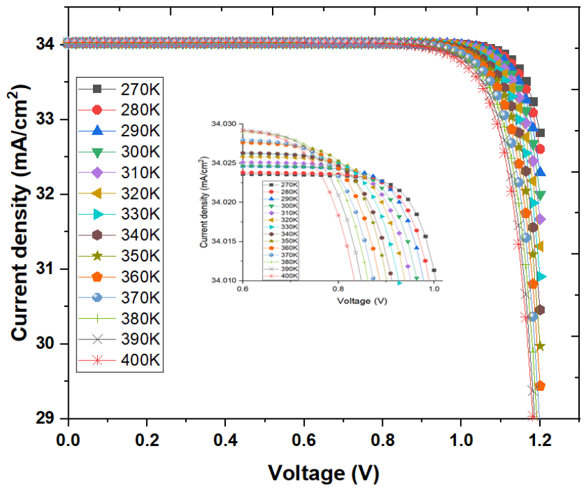
The current density–voltage (J–V) curves of the perovskite solar cells tested throughout a temperature range of 270 K to 400 K are shown in
Figure 2. Every curve has a similar profile, with a plateau at about 34 mA·cm
−2 and a high, almost constant current density in the low-voltage area. The current density steadily lowers as the applied voltage rises and then abruptly drops close to the open-circuit voltage (Voc). This transition region is highlighted in the inset, which clearly shows how the curves vary with temperature, with Voc slightly decreasing as the temperature rises. This trend is characteristic of perovskite solar cells and illustrates how temperature affects the processes of charge transport and recombination.
Figure 2 highlights the influence of temperature on the photovoltaic performance of PSCs, while
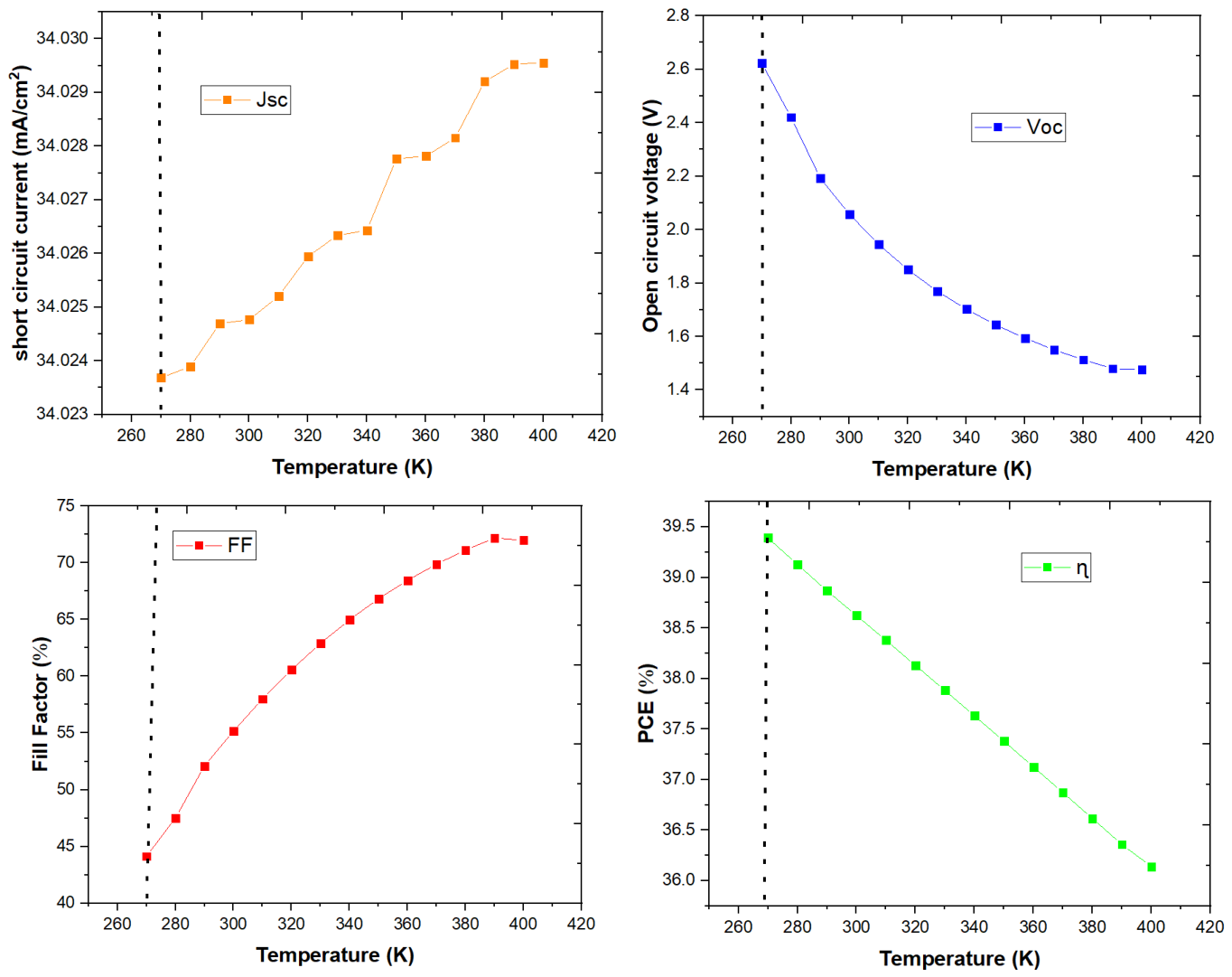
Figure 3 presents the temperature dependence of the main performance parameters, namely the open-circuit voltage (Voc), short-circuit current density (Jsc), fill factor (FF), and power conversion efficiency (PCE). A combination of these parameters determines the device’s efficiency, which is sensitive to temperature changes.
The open-circuit voltage (Voc) decreases progressively with increasing temperature from 270 K to 400 K, following an approximately linear behavior. It decreases significantly from approximately 2.62 V to almost 1.47 V. This decrease has been largely explained by the narrowing of the band gaps at higher temperatures, which reduces the energy difference between the conduction and valence bands. Also, an increase in temperature increases carrier recombination and raises intrinsic carrier concentration, reducing the strength of the internal electric field and, therefore, decreasing Voc.
From a physical perspective, the reduction in Voc with increasing temperature originates from the temperature dependence of the carrier populations and recombination rate described by the drift-diffusion equations solved in SCAPS. As temperature increases, the intrinsic carrier concentration rises, increasing the dark saturation current. Since Voc is logarithmically related to the ratio between the photocurrent and the dark saturation current, the increase in recombination current produces a progressive reduction in the achievable open-circuit voltage. The simulated trend therefore reflects the combined influence of carrier statistics and Shockley–Read–Hall recombination incorporated into the numerical model rather than additional degradation mechanisms [
30].
Conversely, the short-circuit current density (Jsc) does not significantly change during the range of temperatures studied, increasing slightly between about 34.02 mA/cm
2 and about 34.03 mA/cm
2. This small improvement is linked to enhanced carrier generation and mobility at higher temperatures. Nevertheless, the change is not very significant, and it proves that Jsc is comparatively insensitive to changes in temperature as compared to other photovoltaic parameters. The weak temperature dependence of Jsc indicates that photogeneration remains nearly unchanged over the investigated temperature range. Within the SCAPS model, the generation profile is determined primarily by the optical absorption parameters, whereas the slight increase in current results from the improved thermal activation of carrier transport and collection efficiency. Because carrier extraction remains efficient throughout the simulated temperature range, the competing effects of enhanced carrier mobility and increased recombination nearly compensate each other, leading to only minor variations in Jsc [
31].
As illustrated in
Figure 3, the fill factor (FF) increases significantly with temperature, reaching a maximum value of about 72.19% around 390 K. This enhancement can be attributed to minimized internal resistive losses and increased efficiency in charge transportation in the device at moderate temperatures. However, the slight decline at 400 K is reproduced in the SCAPS simulations through the temperature dependence of the electronic transport and recombination parameters included in the model. Since SCAPS does not explicitly simulate material degradation or interface deterioration, this behavior should not be interpreted as direct evidence of thermal degradation but rather as a simulated electrical response under the prescribed temperature-dependent conditions [
23,
32].
Power conversion efficiency (PCE) decreases gradually with temperature, falling between 39.39 and 36.14 percent at 270 and 400 K, respectively, with the major cause of the decrease being the large decrease in Voc. This underscores the crucial role of Voc in determining overall device performance, as its degradation outweighs the positive contributions of the other parameters.
Overall, the performance of PSCs is strongly temperature-dependent. Although FF is sensitive to moderate temperature rises and Jsc is insignificantly affected, the sustained decrease in Voc causes decreased PCE at high temperatures. These results indicate that optimal performance is achieved at lower temperatures, particularly within the 270–300 K range, emphasizing the importance of thermal management and the development of thermally stable materials to ensure efficient and stable operation [
11,
33,
34].
3.2. Complex Impedance Modeling
Impedance Spectroscopy (IS) Analysis
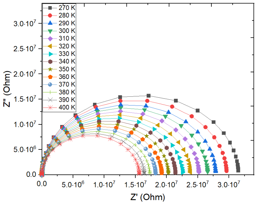
Figure 4 shows the Nyquist plots (Z″ as a function of Z′) recorded for the fabricated perovskite solar cells (PSCs) over the temperature range of 270–400 K. All impedance spectra exhibit a single well-defined semicircular arc, indicating that the electrical response of the device is dominated by a single characteristic process associated with charge carrier transport and recombination. The Nyquist semicircle originates from the characteristic time associated with carrier recombination and transport through the multilayer structure. Within the equivalent-circuit interpretation adopted in this work, the diameter of the semicircle is directly proportional to the effective recombination resistance. As the temperature increases, thermally activated charge carriers enhance transport across the heterojunctions while simultaneously increasing the probability of carrier recombination. Consequently, the effective recombination resistance decreases, shortening the characteristic relaxation time of the device and leading to the progressive contraction of the Nyquist semicircle observed in the simulations. This behavior is fully consistent with the temperature-dependent charge transport and recombination mechanisms incorporated into the SCAPS drift-diffusion model, confirming that the simulated impedance response accurately reflects the underlying physical processes governing device operation [
35]. Within the SCAPS framework, the reduction in the Nyquist semicircle with increasing temperature is explained by the simulated variation in carrier transport and recombination parameters. Although ion migration and defect redistribution have frequently been invoked in experimental studies of perovskite solar cells to explain similar impedance behavior, these mechanisms are not explicitly included in the present SCAPS model. Therefore, they are mentioned only as possible experimental interpretations and not as processes directly demonstrated by the simulations [
36].
Collectively, the simulated impedance response indicates a temperature-dependent evolution of the electronic transport and recombination processes represented in SCAPS. While experimental studies often associate similar impedance changes with coupled ionic-electronic effects, such mechanisms lie beyond the physical model implemented in SCAPS and therefore cannot be confirmed from the present simulations alone [
37].
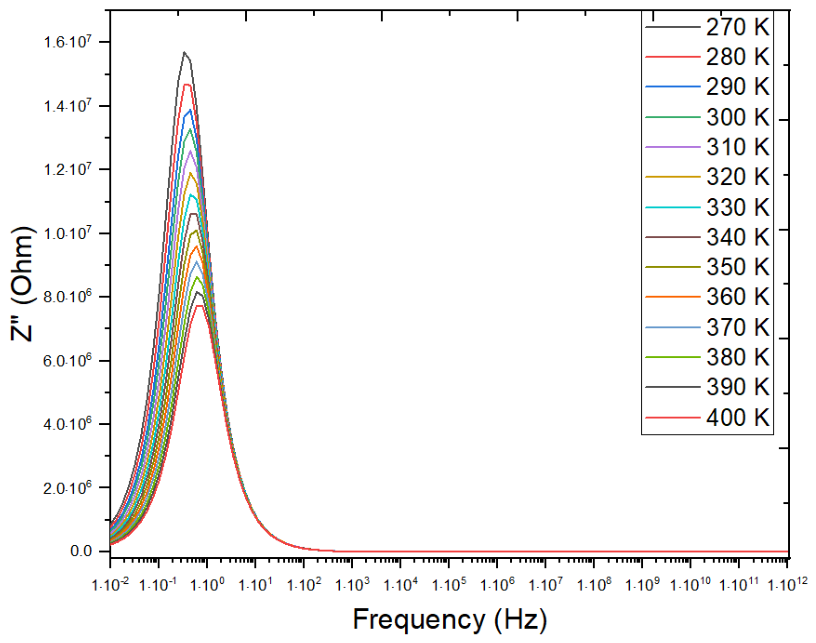
The Nyquist representation provides a global description of the dominant resistive and capacitive processes governing the electrical response of the device. However, it does not explicitly reveal the frequency distribution of these processes. To obtain complementary information regarding the evolution of the characteristic relaxation frequencies and the frequency dependence of the impedance response, the impedance spectra are further analyzed using the Bode representation.
Figure 5 shows the impedance spectrum of perovskite solar cells (PSCs) in the form of Bode plots at different temperatures. Measurements between 270 K and 400 K of the corresponding Nyquist plots always show a single semicircle at each temperature. This finding indicates that charge transport and recombination in the PSCs can be modeled using a simple equivalent circuit model with one predominant recombination pathway. The higher the temperature, the higher the frequency of the maximum of each semicircle, indicating quicker charge carrier dynamics and shorter characteristic relaxation times. In addition, the semicircle diameters decrease with temperature, indicating decreased total impedance and reduced resistive losses-both of which are conducive to more efficient charge transport across the perovskite layer. The observed evolution of the impedance spectra with temperature reflects changes in the effective electrical response predicted by the drift-diffusion model. Possible microscopic mechanisms frequently discussed in the experimental literature, including ionic migration, microscopic heterogeneity, or defect redistribution, are beyond the scope of SCAPS and therefore are not directly resolved in the present simulations [
23]. These results can be compared to those obtained in the past, in which the increase in temperature positively affects ionic mobility and electron-hole recombination [
38,
39]. However, although higher temperatures enhance conductivity and charge transport, they could also lead to a decrease in the structural stability of the perovskite material, which can increase the rate of degradation of the device over time [
40,
41]. The data show that the electrical response of PSCs is extremely sensitive to temperature, supporting the benefits of moderate heating of the material in charge transport and the necessity to maintain thermal conditions to achieve the integrity of the materials.
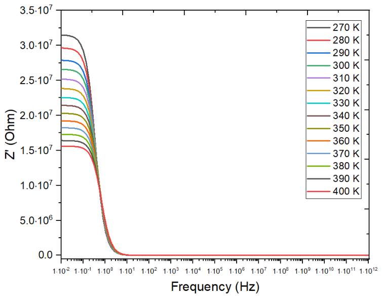
Figure 6 shows the dependency of frequency on the real part of the impedance (Z), in which significant alterations in the slope of the impedance can be found in various frequency ranges, reflecting the existence of varying numbers of relaxation processes in the device.
At very low frequencies (f < 0.1 Hz), Z is nearly constant, indicating strong effects of charge accumulation and polarization at the interface [
42]. A sharp drop in Z is seen in the intermediate frequency range (0.1–10 Hz); this is the regime of carrier mobility and recombination at the perovskite/electrode interfaces [
43]. At even higher frequencies (f > 10 Hz), the impedance approaches a constant, which means that bulk-related processes dominate and capacitive ones gain less influence [
44].
The paper examines how temperature affects the impedance response and photovoltaic characteristics of perovskite solar cells made with CH
3NH
3SnBr
3. Using impedance spectroscopy through Nyquist and Bode analyses, critical parameters like relaxation times and recombination characteristics were established. The Nyquist diagrams always show one semicircle, which proves the claim that the electrical behavior of the devices is dominated by recombination processes. Temperature increases improve charge carrier transport but also increase recombination losses through heightened carrier interactions and activation of defect states, causing a decrease in the open-circuit voltage (Voc) [
45].
The Bode analysis also confirms that there is a single dominant relaxation process and that the characteristic frequency varies with temperature. The impedance response is almost the same at low frequencies, implying that the contribution of ionic migration or deep-level trapping is minimal. Though an increase in temperature initially raises the short-circuit current density (Jsc) due to enhanced photogeneration and carrier mobility, this process levels off at temperatures above 270 K, where recombination mechanisms then dominate, limiting any further increases in efficiency [
46].
These findings are similar to earlier research showing that there is an optimal temperature range in which charge generation and transport are balanced. The fact that the FTO/ETL/CH
3NH
3SnBr
3/Cu
2O structure consistently exhibits a single semicircle under all conditions indicates that interfacial recombination remains the key limiting factor in the FTO/ETL/CH
3NH
3SnBr
3/Cu
2O configuration. Additionally, (Z′) analysis proves the existence of three different regimes: interfacial polarization (at low frequencies), transport-controlled (at intermediate frequencies), and bulk-dominated (at high frequencies) response [
47]. In general, the results highlight the importance of temperature, material characteristics, and interface optimization to enhance charge transport and minimize recombination losses in perovskite solar cells.
The main additional information provided by the impedance analysis is the temperature-dependent evolution of the internal electrical dynamics of the simulated PSC. Unlike the J–V characteristics, which mainly describe the steady-state photovoltaic output, the impedance spectra resolve the frequency-dependent response of the device. In particular, the progressive contraction of the Nyquist semicircle indicates a decrease in the effective recombination resistance with increasing temperature, while the shift in the characteristic frequency toward higher values indicates shorter relaxation times and faster electrical dynamics. The Bode representation provides complementary information on the temperature evolution of the characteristic relaxation frequency, whereas the electric-modulus analysis emphasizes relaxation processes that are less apparent in the conventional impedance representation. These results establish a direct electrical link between temperature, accelerated carrier dynamics, enhanced recombination, and the degradation of photovoltaic performance.
Although the Bode plots clearly identify the characteristic relaxation frequencies associated with the impedance response, they remain strongly influenced by resistive contributions. To further distinguish dielectric relaxation phenomena from electrode polarization effects, the electrical response is subsequently analyzed using the electric modulus formalism. Because the electric modulus is the reciprocal representation of the complex permittivity, it enhances bulk dielectric relaxation while suppressing low-frequency electrode polarization, thereby providing complementary information regarding charge-storage mechanisms within the multilayer structure.
3.3. Complex Modulus Analysis
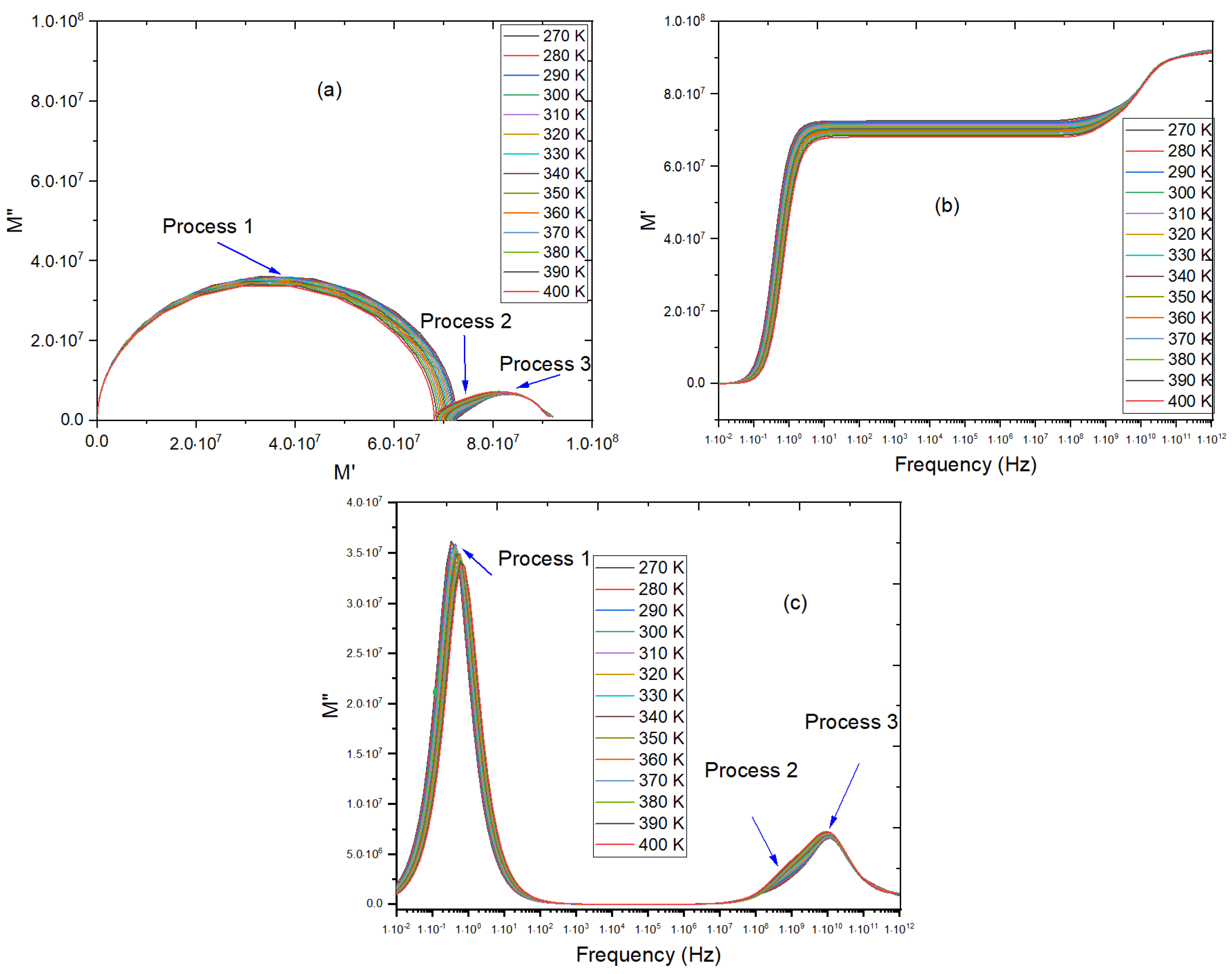
The electric modulus M* is analyzed to obtain a better understanding of the dynamics of the charges by focusing on the contributions of capacitance and significantly reducing artifacts of polarization of the electrode. Three separate peaks can be observed in the imaginary component M″, as illustrated in
Figure 7, which relate to independent relaxation mechanisms, with physical origin and a characteristic range of frequencies. This multi-relaxation is always reflected in both the Nyquist and Bode representations: the Nyquist plots show three resolvable semicircles, indicative of a multi-source impedance response, with charge recombination playing a key role, and the Bode representation of M″ shows that these three processes coexist with three well-separated peak maxima [
48].
The low-frequency relaxation is associated with interfacial polarization and charge accumulation represented by the equivalent electrical response extracted from the simulated impedance spectra. Although low-frequency relaxation in experimental perovskite solar cells is frequently linked to ionic migration or mobile defects, such microscopic mechanisms are not explicitly modeled in SCAPS. Accordingly, the present interpretation is restricted to the equivalent electrical response predicted by the drift-diffusion simulation. Slow ionic entities (especially halide vacancies and tin-related defects) drift under the applied electric field and are stationed at these interfaces, creating space-charge regions. The correspondingly long relaxation time indicates extrinsic ionic effects instead of bulk dielectric effects, as had been previously observed [
49,
50], which showed similar low-frequency characteristics to ion migration mechanisms. The middle-frequency relaxation, which occurs around 10
7–10
8 Hz, is correlated with the dominant electronic processes in the device. This involves both bulk charge transport and recombination within the perovskite and at the heterojunction between the perovskite and the charge-transport layers, particularly the ZnSe ETL and Cu
2O HTL. Its strong dependence on recombination resistance and chemical capacitance suggests that interfacial recombination is a controlling factor in the electrical response and a major efficiency-limiting process, consistent with other results reported in the literature [
51].
High-frequency relaxation (above 10
8 Hz) mainly reflects the dielectric and electronic response represented by the equivalent circuit extracted from the simulated impedance spectra. Since SCAPS does not explicitly describe dipolar reorientation or local ionic motion, these processes cannot be uniquely inferred from the present numerical model. Since this response has a very short characteristic relaxation time, the response is, therefore, characteristic of the fundamental dielectric behavior of the material and is basically independent of interfacial/transport phenomena, in agreement with observations made in [
52].
The observation of the three different relaxation regimes implies that the general impedance behavior is due to a superposition of processes: ionic contributions at low frequencies, charge transport, and recombination processes at intermediate frequencies, and intrinsic dielectric polarization at high frequencies. The latter observations are in agreement with earlier reports, which claimed that there is an optimal temperature of approximately 270 K, at which charge transport and recombination have a good balance [
53]. The ETL/perovskite/Cu
2O structure in the current setup seems to counteract the ion-induced degradation while retaining its ability to collect charge. Thus, the analysis in terms of modulus proves that interfacial recombination is still the major limiting process, which explains the necessity to optimize the interface to enhance the efficiency and stability of perovskite solar cells.
The combined interpretation of the Nyquist, Bode, and electric modulus spectra demonstrates that these representations describe complementary aspects of the same electrical response. While the Nyquist plots identify the dominant resistive and capacitive contributions, the Bode representation characterizes their frequency dependence, and the electric modulus highlights dielectric relaxation processes. These observations provide the physical basis for establishing an equivalent electrical circuit capable of quantitatively reproducing the simulated impedance response and relating the extracted electrical parameters to the underlying transport and recombination mechanisms.
3.4. Equivalent Circuit Analysis of Perovskite Solar Cells
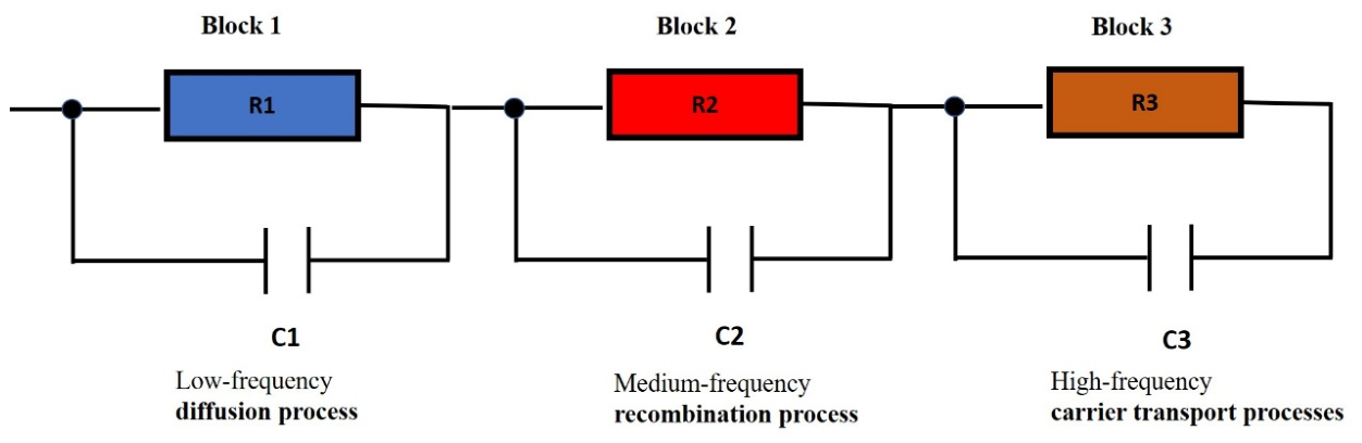
The equivalent circuit was selected according to the principal features observed in the simulated impedance and electric modulus spectra together with the minimum number of electrical elements required to reproduce the simulated frequency response using physically meaningful parameters. Simpler circuit configurations containing only a single RC branch were considered conceptually; however, they cannot adequately represent the multiple relaxation processes identified in the Bode and electric modulus spectra over the investigated temperature range. Consequently, a three-branch equivalent circuit was adopted to account for the distinct electrical processes occurring within different characteristic frequency regions. The selected topology therefore represents the simplest physically consistent model capable of reproducing the simulated impedance response while avoiding unnecessary fitting parameters that could introduce parameter correlation and non-unique solutions. Electrical equivalent circuits provide a convenient macroscopic representation of the complex electrical processes occurring within perovskite solar cells by describing charge transport, recombination, and charge storage through a network of resistive and capacitive elements. The proposed equivalent circuit consists of three parallel RC branches connected in series, as shown in
Figure 8, where the resistance components (R
1, R
2, and R
3) characterize the different transport and recombination losses, while the capacitance components (C
1, C
2, and C
3) describe charge accumulation and dielectric polarization phenomena occurring over different characteristic frequency ranges.
Figure 8 shows the equivalent electrical circuit adopted to represent the simulated impedance response of the perovskite solar cells. The selected circuit topology was chosen because it reproduces the principal features of the simulated Nyquist, Bode, and electric modulus spectra using the minimum number of physically meaningful electrical elements while preserving a clear correspondence between the circuit parameters and the dominant charge transport and recombination mechanisms [
48].
Block 1: The low-frequency domain of diffusion is controlled by the resistance R
1, which represents the dominant low-frequency resistive contribution identified through equivalent-circuit fitting of the simulated impedance spectra. In experimental perovskite solar cells, this contribution is often associated with slow ionic or interfacial processes; however, within the SCAPS framework it should be interpreted as an effective electrical parameter describing the modeled impedance response rather than direct evidence of ion migration. The associated capacitance C
1 records the charge buildup, which occurs due to slow ionic movement, either concentrated at grain boundaries and contact interfaces or spread across the bulk material [
54].
Block 2: R
2 is located in the middle of the frequency scale and is the resistance to recombination used to measure the losses experienced during electron-hole recombination, which directly determines the total photovoltaic performance. The capacitance C
2 reflects charge storage processes that depend on carrier lifetime and carrier transient recombination kinetics in the perovskite absorber [
11].
Block 3: At high frequencies, the charge transport mechanisms that are functional throughout the entire device stack are determined by the R
3, C
3 pair. R
3 is the resistive opposition faced by the charge carriers as they pass through the electron and hole transport layers, and C
3 is the geometric capacitance due to the intrinsic dielectric polarization of the multilayer structure in response to a rapidly alternating electric field [
55].
From a physical standpoint, the equivalent-circuit parameters represent macroscopic electrical quantities that summarize the numerical solution of the drift–diffusion equations implemented in the SCAPS-1D simulations. The resistance components describe the opposition to carrier transport and recombination, whereas the associated relaxation times characterize the temporal response of these electrical processes. Their evolution with temperature therefore provides valuable insight into how thermal energy modifies carrier transport, recombination kinetics, and charge storage within the simulated multilayer structure [
11]. Each RC branch was assigned according to its characteristic frequency domain. The low-frequency branch represents slow electronic processes associated with charge accumulation and recombination, the intermediate-frequency branch reflects carrier transport across the absorber and charge-transport layers, and the high-frequency branch describes the dielectric response together with rapid electronic transport. This frequency-based assignment is consistent with the evolution of the simulated Bode and electric modulus spectra, where distinct relaxation processes become apparent over different frequency ranges.
The equivalent circuit is composed of three parallel RC branches connected in series, where each branch includes a resistance Ri in parallel with a capacitor Ci (for i = 1,2,3).
The impedance of one parallel RC element is a complex expression that can be written as follows:
The relaxation time constant may also be used to reformulate the expression
as follows:
The impedance of the individual branches is therefore
The overall impedance of the circuit is then calculated by adding the contribution of each block, as the three RC elements are in series
The time constant of each RC element is related to its angular frequency by
Alternatively, these quantities can be expressed using the time constants τ
1,τ
2,τ
3, defined as
Relationship between complex impedance and electric modulus.
The complex electric modulus M*(ω) is defined as the reciprocal of the complex permittivity ε*(ω); it can also be formulated in terms of the impedance as
- -
is the complex impedance;
- -
is the geometric capacitance of the sample, with area A and thickness d;
- -
is the angular frequency.
The real and imaginary components of the electric modulus are the “reciprocals” of those of the impedance
The imaginary and real components of the electric modulus are thus directly connected to the values of the impedance and can be viewed as the inverse representation of the impedance in the frequency domain.
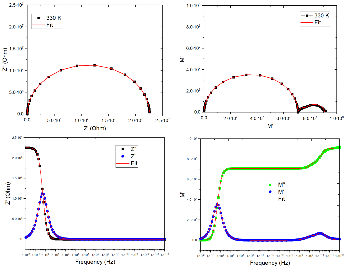
Figure 9 shows that there is a very close correspondence between the experimental impedance and modulus spectra and the fitted curves based on the equivalent circuit model. This consistency testifies to the fact that the offered circuit provides the correct description of the electrical response of the solar cells. In general, the findings confirm the validity of the equivalent circuit method in modeling and explaining the important electrical properties of the devices.
3.5. Equivalent Circuit Analysis and Interpretation
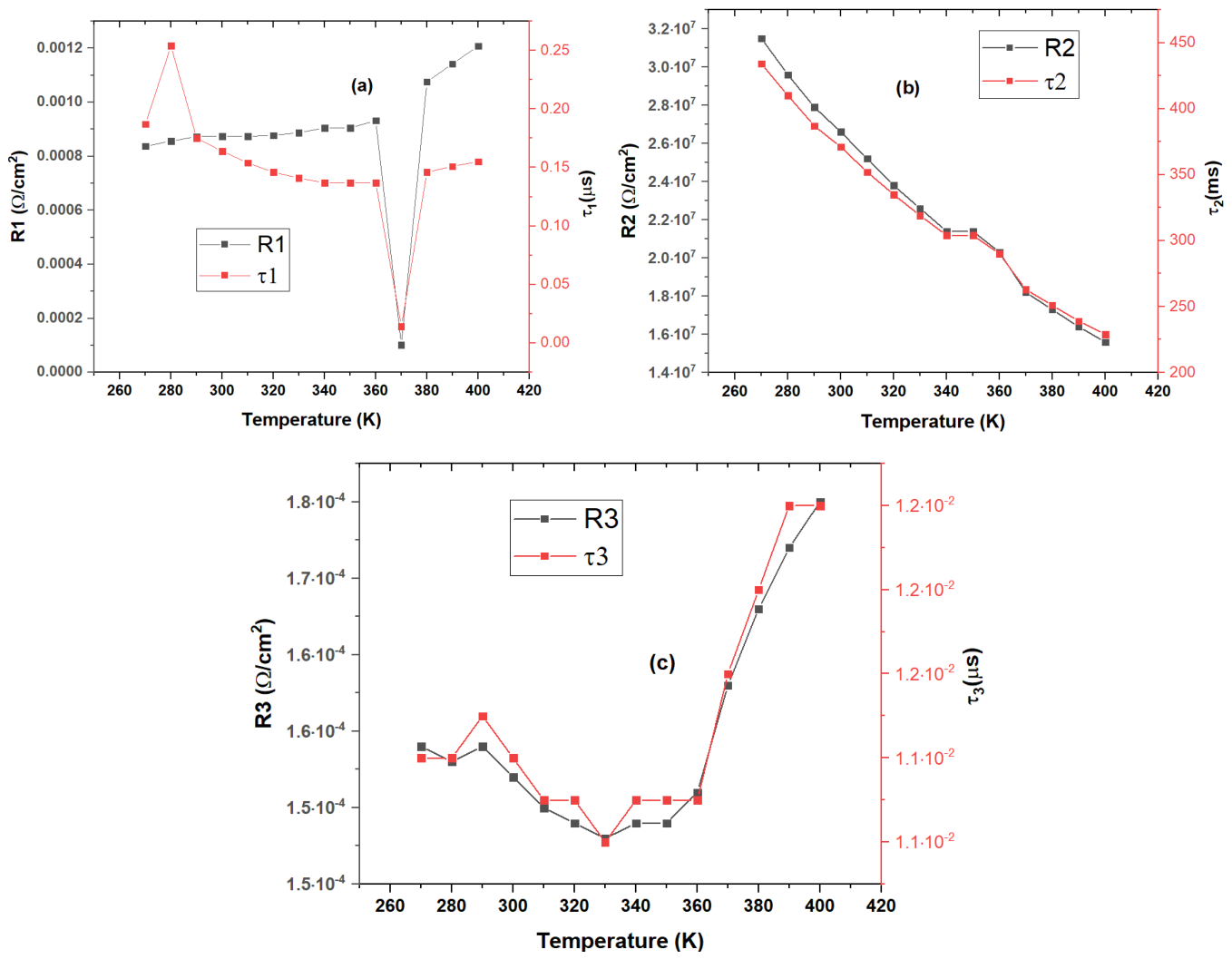
Figure 10 shows the dependence of temperature on the parameters obtained in the equivalent circuit fitting process. The extracted values include the three resistances R
1, R
2, and R
3, along with their corresponding relaxation times τ
1, τ
2, and τ
3, each corresponding to a particular physical process that takes place in a characteristic frequency range of the perovskite solar cell.
Figure 10a illustrates the thermal history of R
1 and τ
1, which are related to the low-frequency ionic diffusion process. Both quantities begin to increase, albeit with a slight rise, up to about 290 K, above which a general downward trend is observed as the heating continues. There is a sharp minimum around 370 K, after which R1 increases rapidly without τ
1 returning to its usual level. This non-monotonic effect is in agreement with a thermally activated transport process, where initially, energy barriers prevent the movement of ions. With increased thermal energy, carrier mobility is increasingly enhanced, which reduces resistance and relaxation time. The anomaly around 370 K reflects a change in the fitted equivalent-circuit parameters obtained from the simulated electrical response. Because SCAPS does not explicitly model structural transitions or defect redistribution, no direct microscopic interpretation is made for this feature. The fact that R
1 and τ
1 develop in parallel over the entire range supports the physical origin of the same relaxation process [
56].
Figure 10b shows the changes in temperature of R
2 and τ
2, which are associated with the intermediate frequency recombination process. The two parameters monotonically decline across the entire temperature scale, which is a clear indication of thermally filled recombination kinetics. The decrease in R
2 is due to a systematic reduction in the resistance to recombination, and the simultaneous decrease in τ
2 indicates a faster recombination dynamic at high temperatures. This can be explained by the increased carrier mobility and a higher likelihood of non-radiative recombination by thermally populated trap states, which increase with temperature [
57].
Figure 10c presents the thermal history of R
3 and τ
3, attributed to the high-frequency charge transport process. The two parameters experience a minor decrease until around 310 K, which aligns with the thermal activation of charge carriers at low temperatures. R
3 shows weak variations, and τ
3 is nearly constant between 310 K and 350 K, indicating a quasi-steady transport regime. Both quantities rise significantly above 350 K, indicating a change in the prevailing mode of transport [
58].
This change is provisionally ascribed to the development of increased ionic contributions or gradual ion concentrations at interfaces, making high-frequency transport more resistive and slower, perhaps representing thermally driven structural rearrangements in the perovskite lattice. Taken together, these data define three temperature regimes of electrical response, ensuring that temperature has differential control over ionic diffusion, charge recombination, and high-frequency transport dynamics in the device.
4. Conclusions
This study investigated the temperature-dependent photovoltaic and impedance response of the FTO/ZnSe/CH3NH3SnBr3/Cu2O perovskite solar cell using the SCAPS-1D drift–diffusion framework over the temperature range of 270–400 K. The J–V results show that the open-circuit voltage (Voc) decreases substantially from approximately 2.62 V at 270 K to 1.47 V at 400 K, whereas the short-circuit current density (Jsc) remains nearly unchanged, varying from approximately 34.02 to 34.03 mA cm−2. The fill factor reaches a maximum of approximately 72.19% around 390 K, while the power conversion efficiency decreases from 39.39% to 36.14%, mainly because of the pronounced reduction in Voc.
The impedance analysis provides information on the internal electrical dynamics that cannot be obtained directly from the J–V characteristics. The progressive contraction of the Nyquist semicircle with increasing temperature indicates a reduction in the effective recombination resistance, while the shift toward higher characteristic frequencies indicates shorter relaxation times and faster electrical dynamics. The Bode and electric-modulus representations further reveal the temperature-dependent relaxation behavior over different frequency ranges.
The equivalent-circuit analysis provides quantitative parameters for describing these changes. In particular, the intermediate-frequency resistance R2 and relaxation time τ2, associated with the dominant recombination response, decrease systematically with increasing temperature, indicating faster recombination kinetics and reduced resistance to recombination. The low-frequency parameters R1 and τ1 exhibit a non-monotonic temperature dependence, whereas the high-frequency parameters R3 and τ3 show relatively weak variations at intermediate temperatures followed by an increase at elevated temperatures. These results demonstrate that temperature affects the different electrical processes of the PSC in distinct ways.
From an engineering perspective, the extracted impedance parameters can serve as effective electrical indicators for evaluating temperature-induced changes in charge transport and recombination. The evolution of R2 and τ2 identifies recombination as an important target for interface and defect optimization, while the high-frequency response provides information relevant to charge transport through the multilayer structure. Consequently, improving the ZnSe/CH3NH3SnBr3 interface, reducing recombination losses, and controlling the operating temperature represent promising strategies for improving the operational performance of CH3NH3SnBr3-based PSCs.
The results should be interpreted within the capabilities of SCAPS-1D. The model does not explicitly include microscopic ion migration, dynamic defect redistribution, phase transitions, structural relaxation, or long-term thermal degradation. Therefore, the extracted equivalent-circuit parameters represent effective macroscopic descriptors of the simulated electrical response rather than direct measurements of microscopic processes. Future experimental impedance measurements combined with multiphysics modeling are recommended to validate these temperature-dependent electrical characteristics and further support the engineering optimization of lead-free CH3NH3SnBr3 PSCs.




 ,
,