
A 13-Bit 100 kS/s Two-Step Single-Slope ADC for a 64 × 64 Infrared Image Sensor


Abstract
1. Introduction
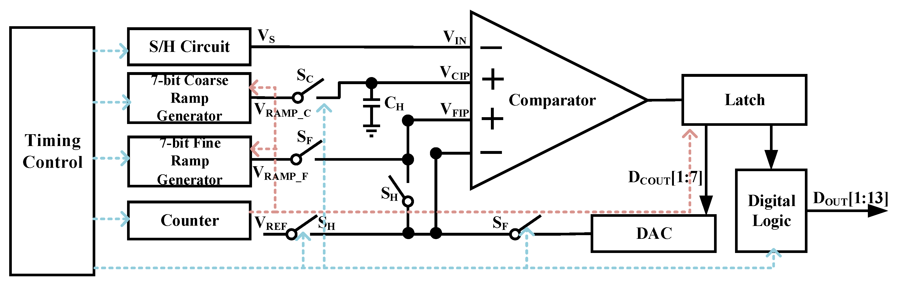
2. Circuit Design
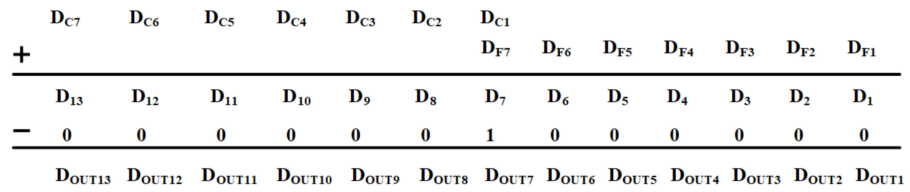
2.1. Quantization Scheme
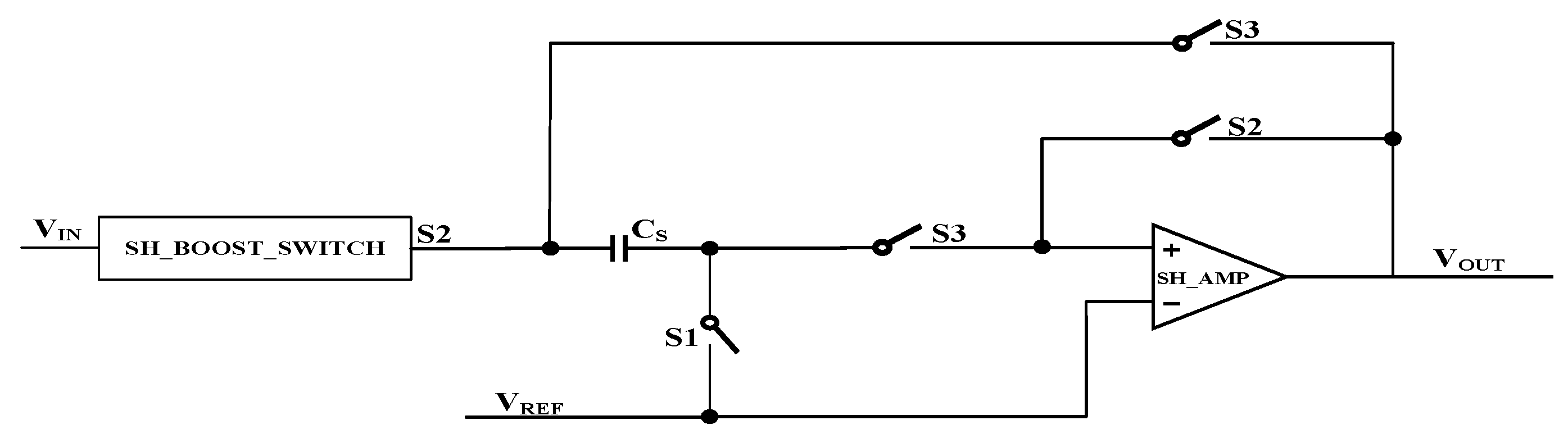
2.2. Sample-and-Hold Circuit
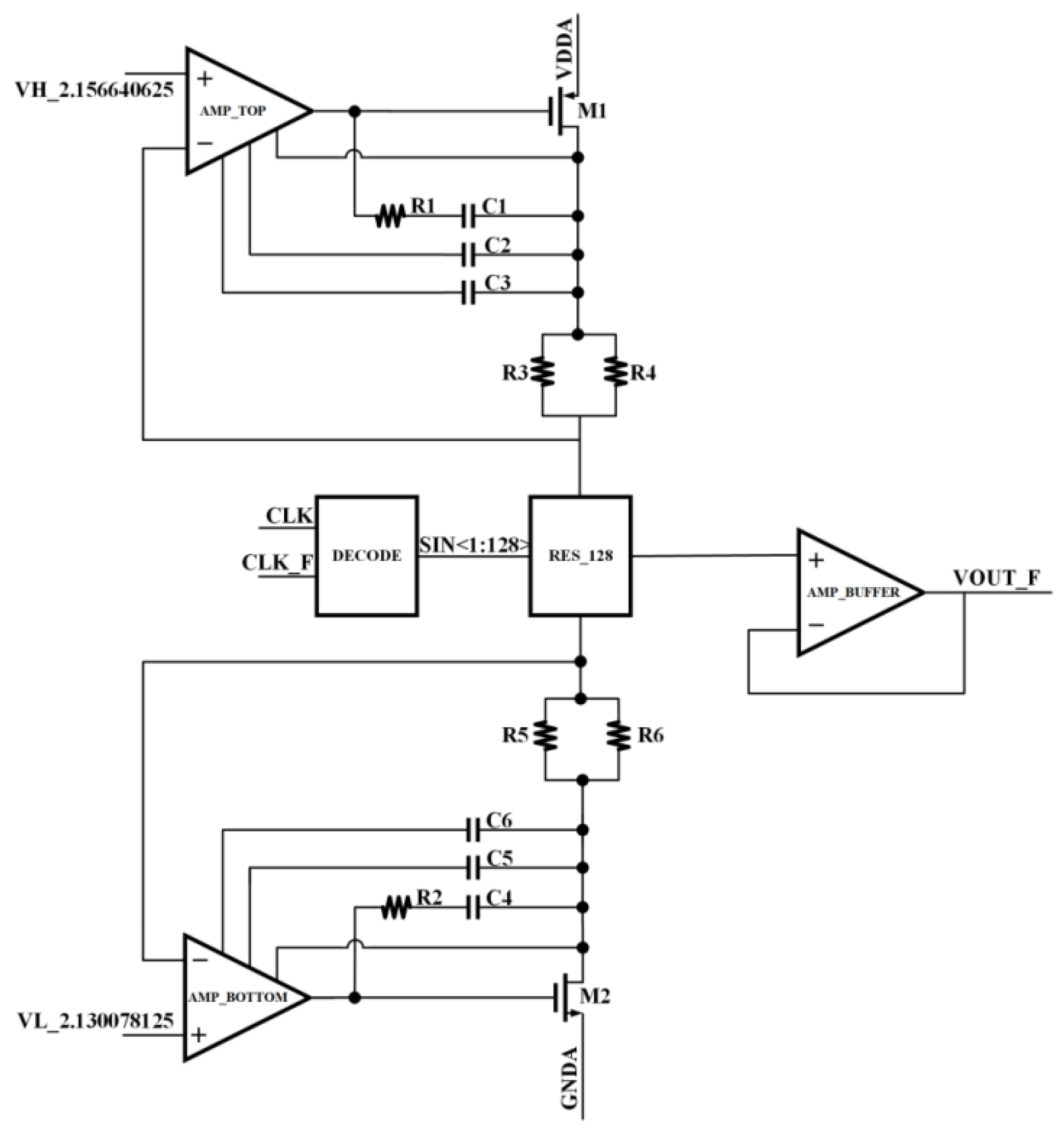
2.3. Coarse Ramp Generator
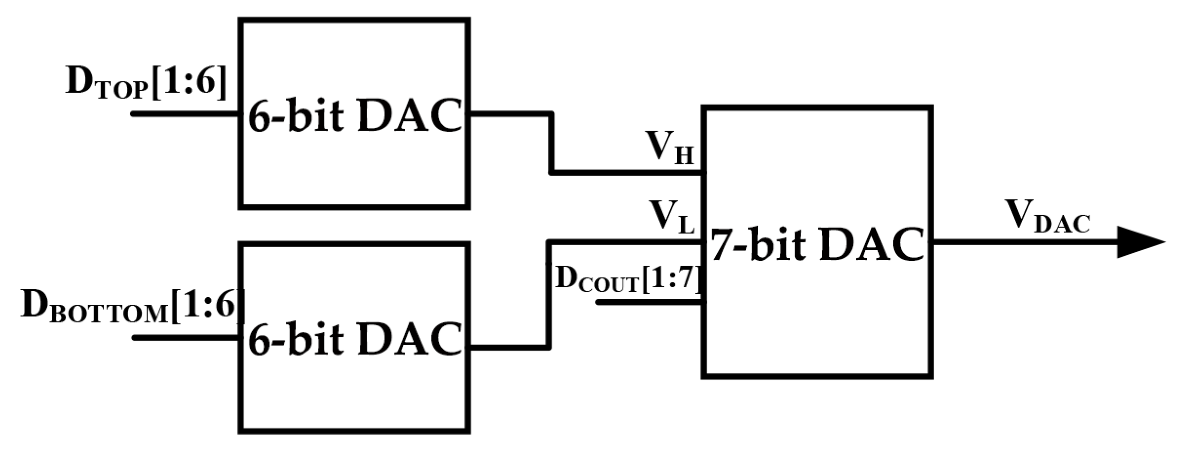
2.4. Fine Ramp Generator
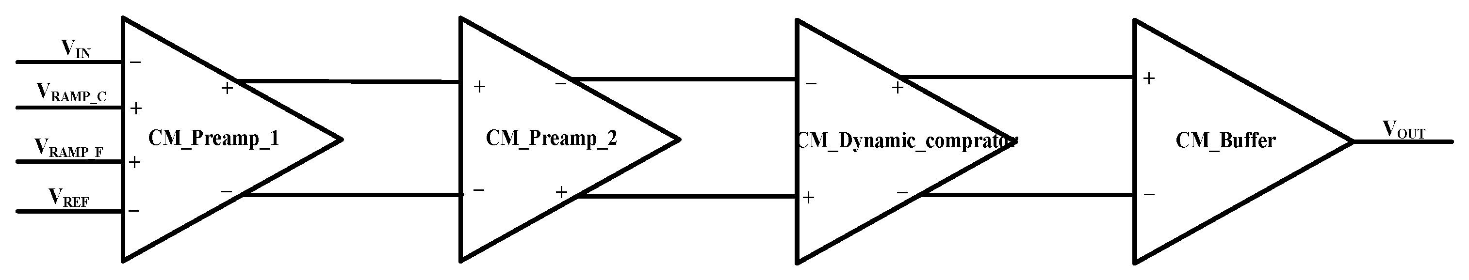
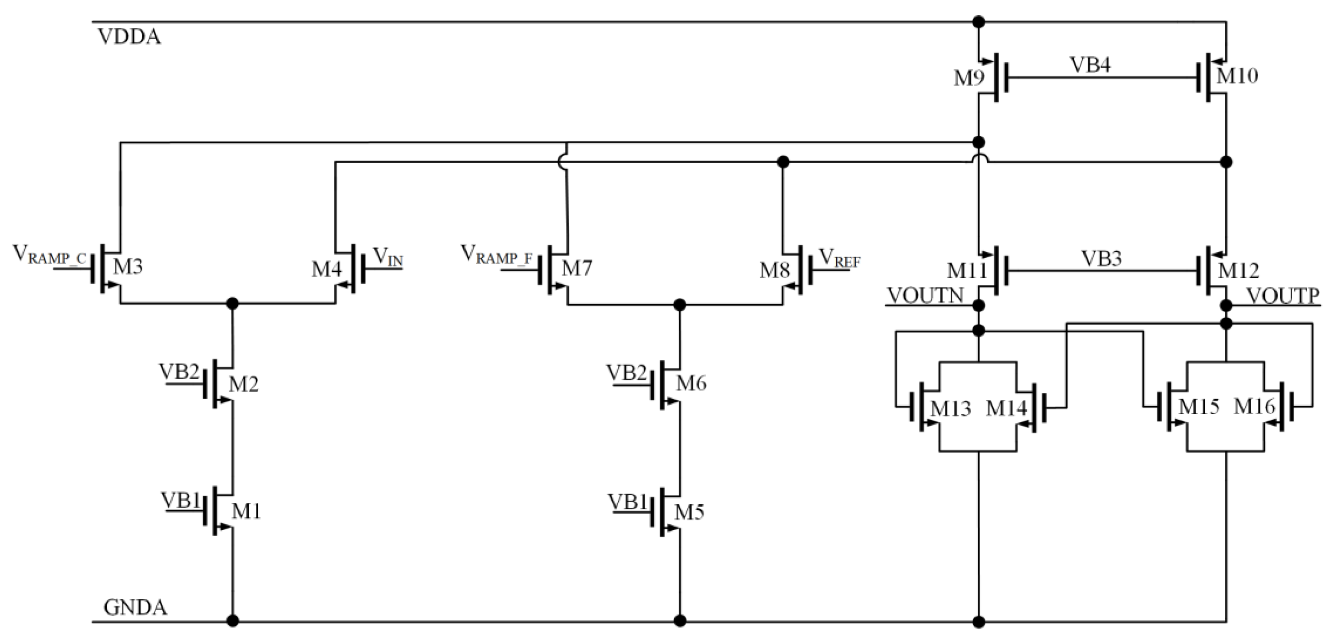
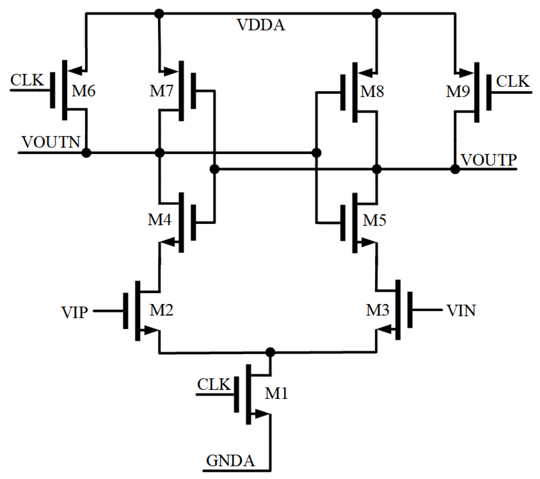
2.5. Comparator
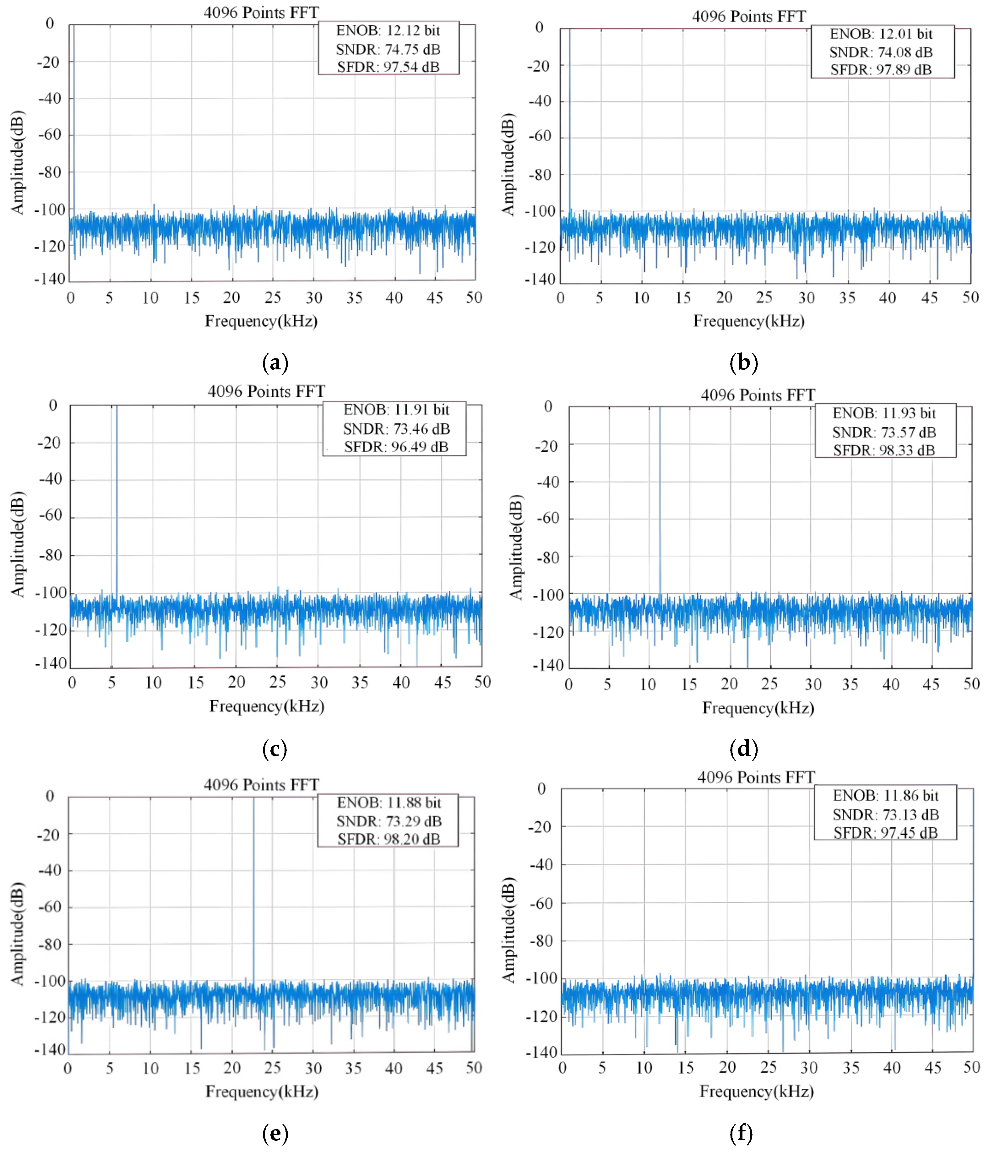
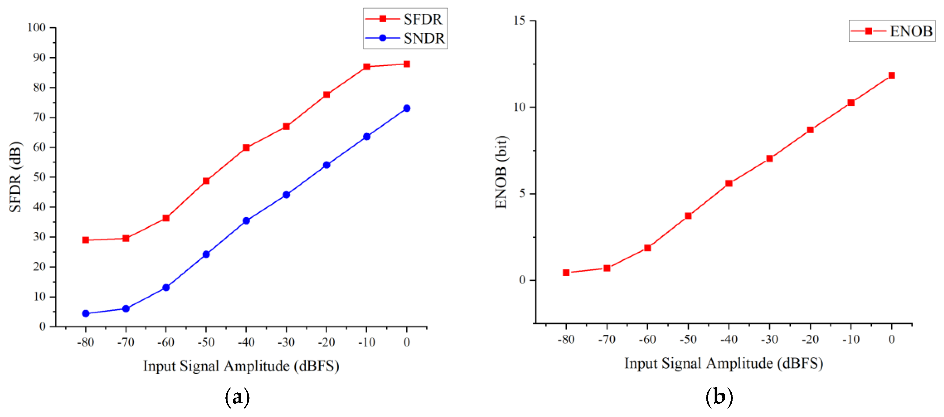
3. Post-Simulation Results
4. Conclusions
Author Contributions
Funding
Institutional Review Board Statement
Informed Consent Statement
Data Availability Statement
Conflicts of Interest
References
- Lyu, T.; Yao, S.; Nie, K.; Xu, J. A 12-Bit High-Speed Column-Parallel Two-Step Single-Slope Analog-to-Digital Converter (ADC) for CMOS Image Sensors. Sensors 2014, 14, 21603–21625. [Google Scholar] [CrossRef] [PubMed]
- McCreary, J.L.; Gray, P.R. All-MOS charge redistribution analog-to-digital conversion techniques. I. IEEE J. Solid-State Circuits 1975, 10, 371–379. [Google Scholar] [CrossRef]
- Decker, S.; McGrath, D.; Brehmer, K.; Sodini, C.G. A 256/spl times/256 CMOS imaging array with wide dynamic range pixels and column-parallel digital output. IEEE J. Solid-State Circuits 1998, 33, 2081–2091. [Google Scholar] [CrossRef]
- Allen, P.E.; Holberg, D.R. CMOS Analog Circuit Design; Oxford University Press: Oxford, UK, 2011. [Google Scholar]
- Snoeij, M.F.; Theuwissen, A.J.P.; Huijsing, J.H.; Makinwa, K.A.A. Power and Area Efficient Column-Parallel ADC Architectures for CMOS Image Sensors. In Proceedings of the 2007 IEEE Sensors, Atlanta, GA, USA, 28–31 October 2007; IEEE: Piscataway, NJ, USA, 2007; pp. 523–526. [Google Scholar] [CrossRef]
- Lim, S.; Lee, J.; Kim, D.; Han, G. A High-Speed CMOS Image Sensor with Column-Parallel Two-Step Single-Slope ADCs. IEEE Trans. Electron Devices 2009, 56, 393–398. [Google Scholar] [CrossRef]
- Bae, J.; Kim, D.; Ham, S.; Chae, Y.; Song, M. A Two-Step A/D Conversion and Column Self-Calibration Technique for Low Noise CMOS Image Sensors. Sensors 2014, 14, 11825–11843. [Google Scholar] [CrossRef] [PubMed]
- Huang, W.; Zhang, Q.; Li, J.; Zhang, Z.; Deng, H.; Ning, N.; Yu, Q. A Calibration Technique for Two-Step Single-Slope Analog-to-Digital Converter. In Proceedings of the 2019 IEEE 13th International Conference on ASIC (ASICON), Chongqing, China, 29 October–1 November 2019; pp. 1–4. [Google Scholar] [CrossRef]
- Zhang, H.; Fang, Z.; Yu, N.; Lv, N.; Guo, Z. A Column-parallel SAR/SS ADC with Multi-Column Shared Capacitor DAC for CMOS Image Sensor. In Proceedings of the 2022 IEEE 16th International Conference on Solid-State & Integrated Circuit Technology (ICSICT), Nangjing, China, 25–28 October 2022; pp. 1–3. [Google Scholar] [CrossRef]
- Park, W.; Piao, C.; Lee, H.; Choi, J. CMOS Image Sensor with Two-Step Single-Slope ADCs and a Detachable Super Capacitive DAC. IEEE Trans. Circuits Syst. II Express Briefs 2022, 69, 849–853. [Google Scholar] [CrossRef]
- Shin, M.-S.; Kwon, O.-K. 14-bit two-step successive approximation ADC with calibration circuit for high-resolution CMOS imagers. Electron. Lett. 2011, 47, 790–791. [Google Scholar] [CrossRef]
- Tang, F.; Chen, D.G.; Wang, B.; Bermak, A. Low-Power CMOS Image Sensor Based on Column-Parallel Single-Slope/SAR Quantization Scheme. IEEE Trans. Electron Devices 2013, 60, 2561–2566. [Google Scholar] [CrossRef]
- Lee, J.; Park, H.; Song, B.; Kim, K.; Eom, J.; Kim, K.; Burm, J. High Frame-Rate VGA CMOS Image Sensor Using Non-Memory Capacitor Two-Step Single-Slope ADCs. IEEE Trans. Circuits Syst. I Regul. Pap. 2015, 62, 2147–2155. [Google Scholar] [CrossRef]
- Li, S.; Qiao, B.; Gandara, M.; Pan, D.Z.; Sun, N. A 13-ENOB Second-Order Noise-Shaping SAR ADC Realizing Optimized NTF Zeros Using the Error-Feedback Structure. IEEE J. Solid-State Circuits 2018, 53, 3484–3496. [Google Scholar] [CrossRef]
- Snoeij, M.F.; Theuwissen, A.J.P.; Makinwa, K.A.A.; Huijsing, J.H. Multiple-Ramp Column-Parallel ADC Architectures for CMOS Image Sensors. IEEE J. Solid-State Circuits 2007, 42, 2968–2977. [Google Scholar] [CrossRef]
- Nuzumlalı, O.L.; Karalar, T.C. A Current Calibration Circuit for a 14-Bit Column-Parallel Dual-Ramp Single-Slope ADC in Infrared Image Sensors. IEEE Trans. Circuits Syst. II Express Briefs 2024, 71, 4824–4828. [Google Scholar] [CrossRef]
- Fang, D.; Nie, K.; Zhang, Z.; Xu, J. Two-Step Single-Slope ADC Utilizing Differential Ramps for CMOS Image Sensors. Circuits Syst. Signal Process 2024, 43, 6097–6114. [Google Scholar] [CrossRef]
- Zhang, B.; Yang, C.; Chen, N.; Chen, J.; Hu, Z.; Wang, G.; Feng, P.; Liu, J.; Wu, N.; Liu, L. A Novel Hybrid Dual Ramp Generator for Two-Step Single-Slope ADCs in CMOS Image Sensors. In Proceedings of the 2024 6th International Conference on Circuits and Systems (ICCS), Chengdu, China, 20–23 September 2024; pp. 185–188. [Google Scholar] [CrossRef]
- Xu, R.; Guo, Z.; Cheng, X.; Su, C.; Li, C.; Wang, Y. A 13-Bit High Speed Two-Step Single Slope ADC Design Method for Hundreds of Mpxiel CMOS Image Sensors. In Proceedings of the 2022 IEEE 5th International Conference on Electronics Technology (ICET), Chengdu, China, 13–16 May 2022; pp. 147–151. [Google Scholar] [CrossRef]
- Zhang, Q.; Ning, N.; Li, J.; Yu, Q.; Wu, K.; Zhang, Z. A 12-Bit Column-Parallel Two-Step Single-Slope ADC With a Foreground Calibration for CMOS Image Sensors. IEEE Access 2020, 8, 172467–172480. [Google Scholar] [CrossRef]
- Park, H.; Yu, C.; Kim, H.; Roh, Y.; Burm, J. Low Power CMOS Image Sensors Using Two Step Single Slope ADC With Bandwidth-Limited Comparators & Voltage Range Extended Ramp Generator for Battery-Limited Application. IEEE Sens. J. 2020, 20, 2831–2838. [Google Scholar] [CrossRef]
- Nie, K.; Zha, W.; Shi, X.; Li, J.; Xu, J.; Ma, J. A Single Slope ADC With Row-Wise Noise Reduction Technique for CMOS Image Sensor. IEEE Trans. Circuits Syst. I Regul. Pap. 2020, 67, 2873–2882. [Google Scholar] [CrossRef]


| Coarse Quantization Resolution | Fine Quantization Resolution | Coarse Quantization Cycles | Fine Quantization Cycles | Total Cycles |
|---|---|---|---|---|
| 6-bit | 7 + 1-bit | 64 | 256 | 320 |
| 7-bit | 6 + 1-bit | 128 | 128 | 256 |
| 8-bit | 5 + 1-bit | 256 | 64 | 320 |
| [18] | [19] | [20] | [21] | [9] | [22] | This Work | |
|---|---|---|---|---|---|---|---|
| Process (nm) | 110 | 55 | 130 | 90 | 110 | 110 | 55 |
| Supply voltage (V) | 3.3/1.5 | 3.3 | 3.3/1.2 | 2.8/1.5 | 3.3/1.2 | 3.3/1.5 | 3.3 |
| Structure | TS-SS | TS-SS | TS-SS | TS-SS | SAR-SS | SS | TS-SS |
| Transition time (μs) | 2 | 0.512 | 10 | 39.7 | - | 34.2 | 10 |
| Quantization range (V) | 2 | 1.7 | 1.2 | 1 | 2 | 1 | 1.7–3 |
| Resolution (bit) | 10 | 13 | 12 | 12 | 12 | 10 | 13 |
| ENOB (bit) | - | 11.33 | 11.25 | - | 11.17 | 8.8 | 11.86 |
| FoM (J/step) | - | 9.35 f | 296 f | - | - | 4.3 p | 59.7 p |
Disclaimer/Publisher’s Note: The statements, opinions and data contained in all publications are solely those of the individual author(s) and contributor(s) and not of MDPI and/or the editor(s). MDPI and/or the editor(s) disclaim responsibility for any injury to people or property resulting from any ideas, methods, instructions or products referred to in the content. |
© 2025 by the authors. Licensee MDPI, Basel, Switzerland. This article is an open access article distributed under the terms and conditions of the Creative Commons Attribution (CC BY) license (https://creativecommons.org/licenses/by/4.0/).
Share and Cite
Gan, Q.; Liao, W.; Zheng, W.; Yu, E.; Chen, Z.; Chen, C. A 13-Bit 100 kS/s Two-Step Single-Slope ADC for a 64 × 64 Infrared Image Sensor. Eng 2025, 6, 180. https://doi.org/10.3390/eng6080180
Gan Q, Liao W, Zheng W, Yu E, Chen Z, Chen C. A 13-Bit 100 kS/s Two-Step Single-Slope ADC for a 64 × 64 Infrared Image Sensor. Eng. 2025; 6(8):180. https://doi.org/10.3390/eng6080180
Chicago/Turabian StyleGan, Qiaoying, Wenli Liao, Weiyi Zheng, Enxu Yu, Zhifeng Chen, and Chengying Chen. 2025. "A 13-Bit 100 kS/s Two-Step Single-Slope ADC for a 64 × 64 Infrared Image Sensor" Eng 6, no. 8: 180. https://doi.org/10.3390/eng6080180
APA StyleGan, Q., Liao, W., Zheng, W., Yu, E., Chen, Z., & Chen, C. (2025). A 13-Bit 100 kS/s Two-Step Single-Slope ADC for a 64 × 64 Infrared Image Sensor. Eng, 6(8), 180. https://doi.org/10.3390/eng6080180