1. Introduction
Developments in ultra-fast high-power solid-state switches are pushing the limits of semiconductor devices, enabling the development of full solid-state pulsed power systems that take advantage of the reliability, long lifetime, and precise controllability offered by this technology. In particular, Power Drift Step Recover Diodes (DSRDs) and Semiconductor Opening Switches (SOSs) have driven significant progress in nanosecond pulse generation systems achieving current slew rates over 100 kA/
s and peak power levels above 100 MW [
1,
2,
3]. These technological breakthroughs require precise sensing systems for diagnosing and monitoring signal integrity. However, as devices become faster and capable of operating with higher working voltages, the use of traditional voltage sensors, like resistive divider probes, becomes impractical. For instance, two popular high-voltage probes on the market, such as the Tektronix P6015A (Max VDC = 20 kV, BW = 75 MHz) [
4] and the Keysight 10076C (Max VDC = 3.7 kV, BW = 500 MHz) [
5], are only capable of accurately reproducing signals with rise-times greater than 4.7 ns and 0.7 ns, respectively. As a result, their use is restricted when sensing sub-nanosecond pulse signals. This limitation, in addition with the growing demand for non-invasive and cost-effective sensors, emphasizes the need for new sensing technologies suited for modern high-speed pulsed systems.
To answer these new requirements, several efforts have explored the development of PCB-integrated sensors, including Rogowski coil current sensors proposed in [
6,
7,
8] and D-dot sensors such as the one developed in [
9]. In this context, planar sensors have also emerged as promising candidates for non-contact voltage measurements due to their compatibility with printed circuit boards (PCBs).
However, the technology remains underexplored, and prior efforts have revealed trade-offs between high bandwidths and sensor responsivity [
9,
10]. The planar voltage sensor first introduced in [
10], while effective, is a good example of this trade-off as it struggles to achieve high bandwidths to accurately capture fast transient signals, compromising sensing accuracy at GHz frequencies or sub-nanosecond transients.
2. Background
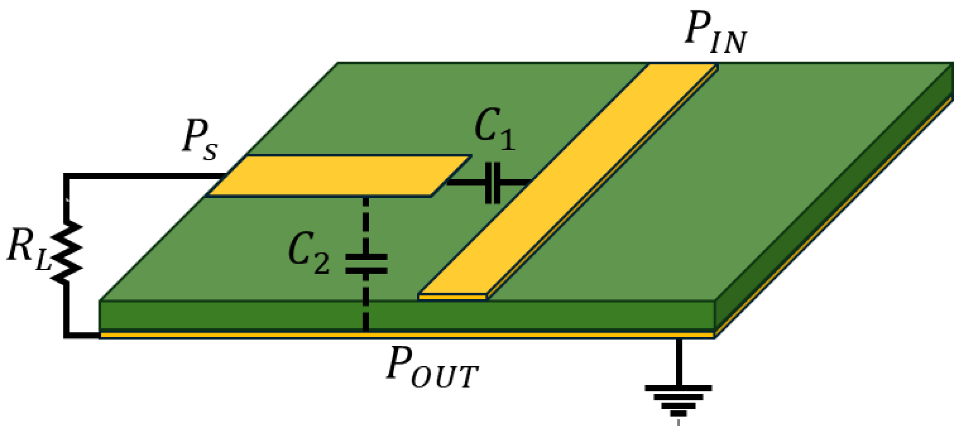
A D-dot is an electric sensor that measures the time derivative of the electric displacement field to produce a voltage at its output terminals. These displacement field perturbations are closely related to voltage variations, which is why D-dots are often used as derivative voltage sensors, also known as V-dots. The derivative nature of a planar D-dot sensor is modeled using the capacitive coupling between the sensor’s head and the observed current-carrying conductor as shown in
Figure 1. The sensor voltage gain transfer function is shown in Equation (
1), where
is the capacitance between the D-dot and the power trace,
is the sensor’s capacitance to ground, and
is the termination impedance, often assumed as 50
[
9,
11,
12].
This model then predicts two operational modes depending on the frequency band: the derivative mode for , where the sensor’s output is linearly dependent on the time derivative of the sensed signal, and the self-integrating mode that occurs when , where the output is proportional to the amplitude of the sensed signal.
It is the wide-band characteristic of the derivative mode that makes D-dots ideal for measuring pulsed signals with broad spectral content.
When operating in derivative mode, the responsivity of the sensor,
, correlates the sensor’s output voltage
and the time derivative of the sensed signal
, as follows:
This responsivity is directly related to the frequency response of the sensor
[
9,
13] and can be correlated with the following expression.
where
is the responsivity of the sensor in decibels,
is an angular frequency below the low frequency limit of the sensor, and
is the magnitude of the frequency response of the sensor as given in Equation (
1). It is worth mentioning that Equations (
2) and (
3) are only valid under low-frequency approximation where the sensor operates in its derivative mode.
In [
10], a planar D-dot based on the geometry of a microstrip line was introduced. The sensor was constructed by terminating a 50
microstrip line with a “pad” to increase its responsivity. The pad was formed by a 50
microstrip transmission line with semicircular caps, as shown in
Figure 2. The length of the pad (
L) and the gap distance (
d) were varied, and it was demonstrated how both parameters affected both the bandwidth and sensitivity of the planar sensor making it suitable for parametric optimization. This investigation studies the geometry dependence of the sensor by exploring the influence of the pad shape while eliminating the imposed impedance constraint on the sensor’s pad.
Figure 2 shows a schematic representation of the planar sensor test fixture. In this setup, a signal is injected into port
and propagates through a 50
microstrip line until it reaches the output port
. The sensor’s head is positioned along the current-carrying line to detect displacement field perturbations caused by the propagating wave. These perturbations induce a voltage signal, which is then measured at port
. An optimization procedure was developed, employing both simulation and signal processing techniques available in the simulation software CST Studio 2022 [
14], to determine how changes in the sensor design impact its bandwidth.
3. Materials and Methods
The optimization procedure is described as follows: An exponential voltage step with the form
and a 35 ps rise time (
GHz) is injected into the input port (
) of a 50
microstrip line, where it propagates until it reaches the output port (
) (see
Figure 3). A planar D-dot sensor, placed along one side of the main line, senses variations in the displacement field caused by the propagating wave. The sensor signal is transmitted through another 50
microstrip section to the sensing port (
), where it is measured and numerically integrated to recover the input pulse.
The 10–90 rise time (
) of the recovered signal is then measured to determine the sensor’s bandwidth (
), as seen in Equation (
4) [
15]:
If the D-dot bandwidth is sufficiently broad to cover the majority of the input pulse spectral range—specifically, when the sensor’s bandwidth is three to five times greater than the maximum frequency of interest in the sensed signal [
16,
17,
18]—then rise times of both sensed and recovered pulses will match. Otherwise, the recovered signal will exhibit a longer rise time due to attenuation of its high-frequency components during numerical integration [
19].
The rise-time of the recovered signal is then used as a metric for sensor performance. When the recovered signal’s rise-time is below the target of 35 ps, the sensor’s geometric parameters are updated using CST Studio’s built-in optimization tool, which employs a covariance matrix adaptation evolution strategy (CMA-ES) [
20] to further enhance bandwidth.
For this study, the sensors were fabricated on a TMM4 substrate from Rogers Corporation with relative permittivity
and loss tangent
at 10 GHz [
21], and a gap distance (
d) of 5 mm was established between the sensor’s head and the current-carrying trace to provide a theoretical hold-off voltage of ∼16 kV [
11] (see
Figure 2). Two different sensor geometries were explored independently in the pursuit of an optimal design; their bandwidth and time-domain response were characterized and compared throughout the process.
3.1. Parameter Optimization of Free-Geometry (Spline) Sensor
Inspired by the broadband characteristics of the planar bowtie antenna, where shape modifications have been shown to extend their operational frequency range [
22,
23,
24], it was hypothesized that modifying the pad shape of the voltage planar sensor could enhance its frequency response. Although the initial design is entirely different from a bowtie, previous studies motivated the exploration of a distinctive geometry aimed at maximizing the sensor’s bandwidth.
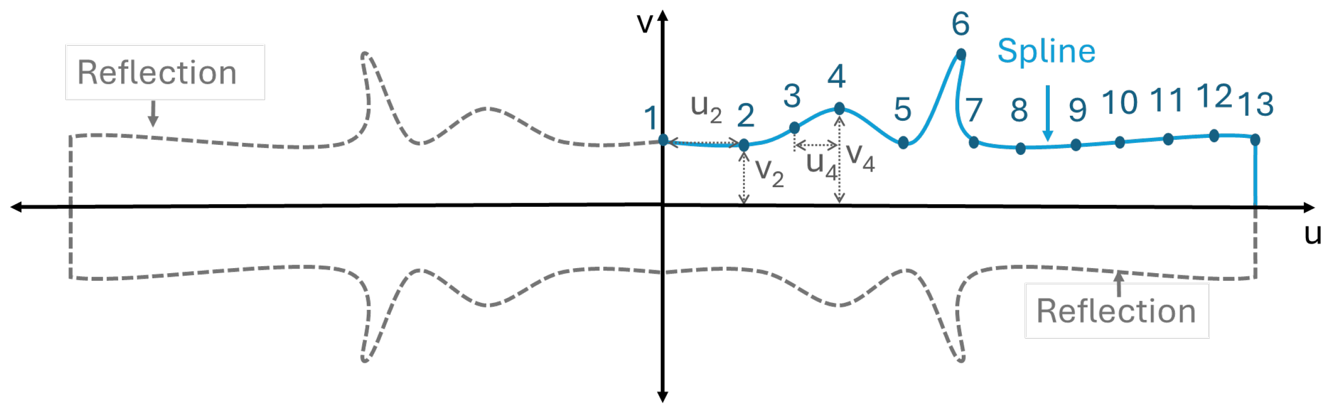
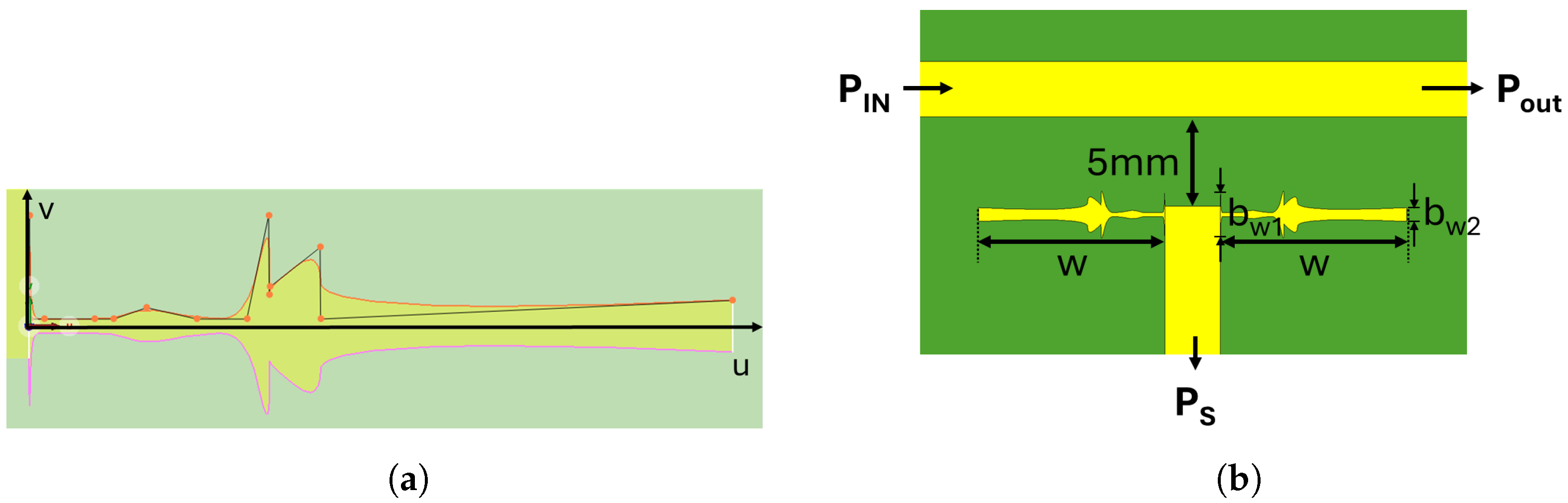
The first proposed design uses the padded sensor as the parent geometry but replaces the pad shape with a custom closed contour. The new sensor pad was created using CST studio’s native Spline tool, which draws a piecewise polynomial curve interpolating thirteen independent Cartesian points to create a part of the sensor contour in the first quadrant of a
-plane (see
Figure 4). This contour is then mirrored across both axes to generate a symmetric sensor pad that is placed on either side of a transmission line connected to the sensing port (
), as shown in
Figure 5b.
The number of coordinate points was set arbitrarily and was intended to provide sufficient degrees of freedom for the optimization algorithm to find a solution within a broad solution space.
The optimization problem that maximizes the sensor’s bandwidth is defined in Equation (
5).
where
is the bandwidth function of the sensor controlled by the geometric parameters
x. Variables
through
control the spacing in the
u direction between points, while
through
represent the spacing in the
v direction of each point. The variable
w defines the overall length of the spline section in the
u direction, and
and
control the width of the spline surface at the origin and the end of the surface, respectively. The optimized design was fabricated in a ProtoLaser system by LPKF to guarantee machining accuracy.
The sensor’s frequency response was measured within the region of interest, spanning 10 MHz to 6 GHz, using a 67 GHz VNA N5247A (Keysight, Santa Rosa, CA, USA) [
25]. The measurement process included matching the port
with a broadband 50
load to prevent reflections, allowing the characterization of the D-dot sensor using a two-port s-parameter matrix between ports (
) rather than using a three-port matrix between all ports (
) [
26]. The obtained s-parameters where later converted to
to determine the voltage gain of the sensor.
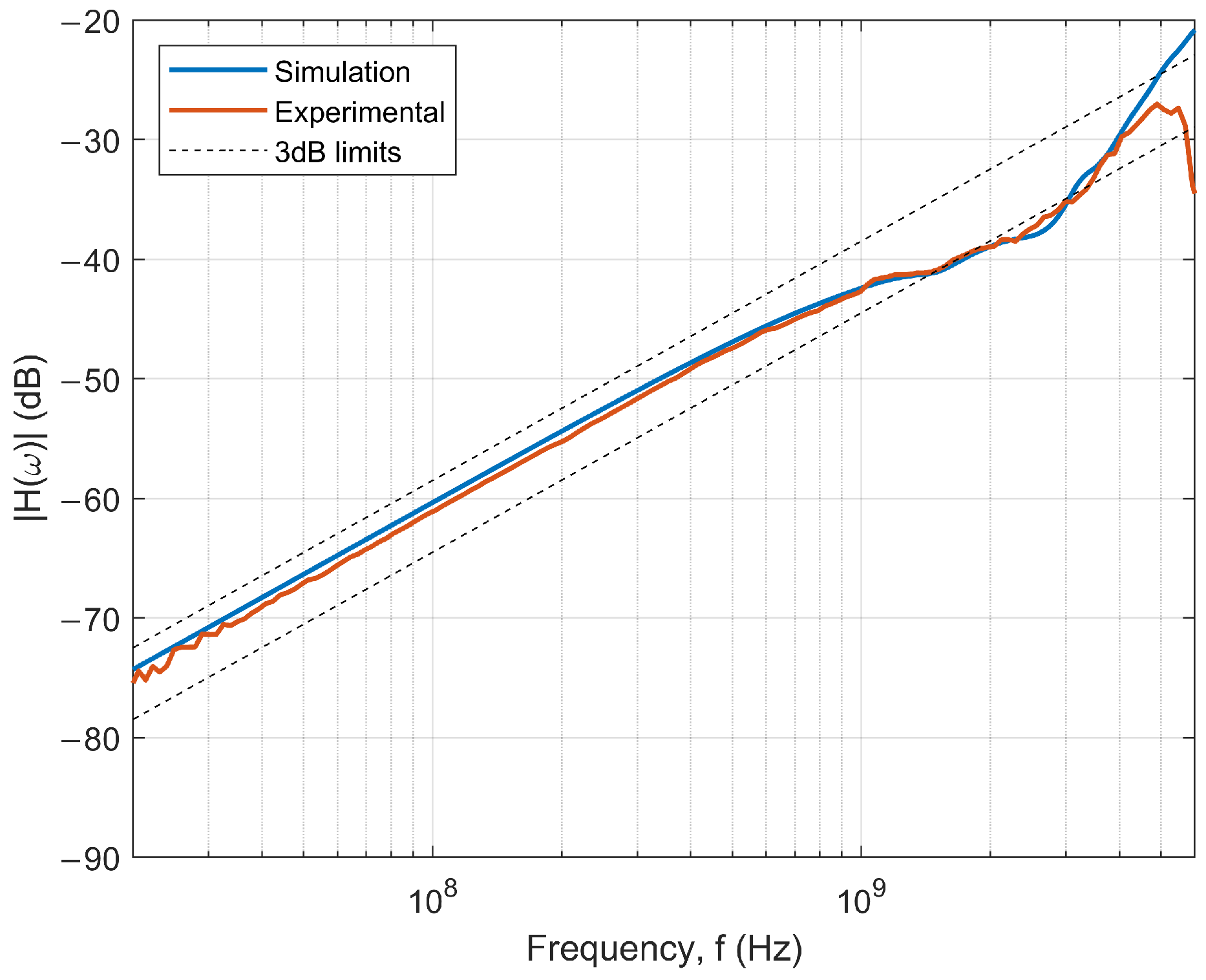
The frequency response of the optimized sensor is depicted in
Figure 6. The good agreement between the simulated response and the experimental measurements within the area of interest provides confidence in the numerical simulation method and the optimization algorithm.
The set of parameters that describe the optimized sensor’s profile are shown in
Table A1 in
Appendix A.
The resulting sensor geometry exhibits clear derivative mode behavior through most of the frequency range, highlighting its potential as a broadband voltage sensor. Nonetheless, the sensor features a complex geometry with elements as small as 30 m, which are not only difficult to reproduce without specialized manufacturing equipment but also contribute to localized field enhancements that may reduce the sensor’s hold-off voltage.
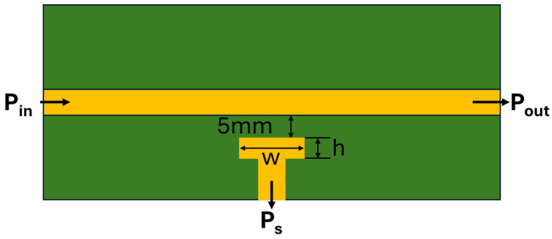
3.2. Parameter Optimization of Padded (T-Shape) D-Dot Sensor
The Spline sensor demonstrated the effectiveness of parametric optimization to planar D-dot sensors, but the complexity and sharp edges of the realized topology limits its manufacturability and potentially reduces its maximum operational voltage. Thus, a second, simpler sensor geometry was investigated. In this design, the sensor profile was limited to a straight metal section (the sensor’s head) placed parallel to the current-carrying line, with a 50
microstrip line running orthogonally from the sensor’s head to the sensing port (
). This sensor profile resembled the letter “T” and was therefore named “T-shape” to distinguish it from the padded sensor (See
Figure 7).
The objective function that maximizes the bandwidth of this sensor was formally defined as follows.
In this formulation,
x is the set of geometric variables to be optimized to maximize the sensor’s bandwidth
,
w represents the overall length of the sensor’s head, and
h defines its thickness. The final parameters of the optimized T-shape sensor are provided in
Table A2 in
Appendix A.
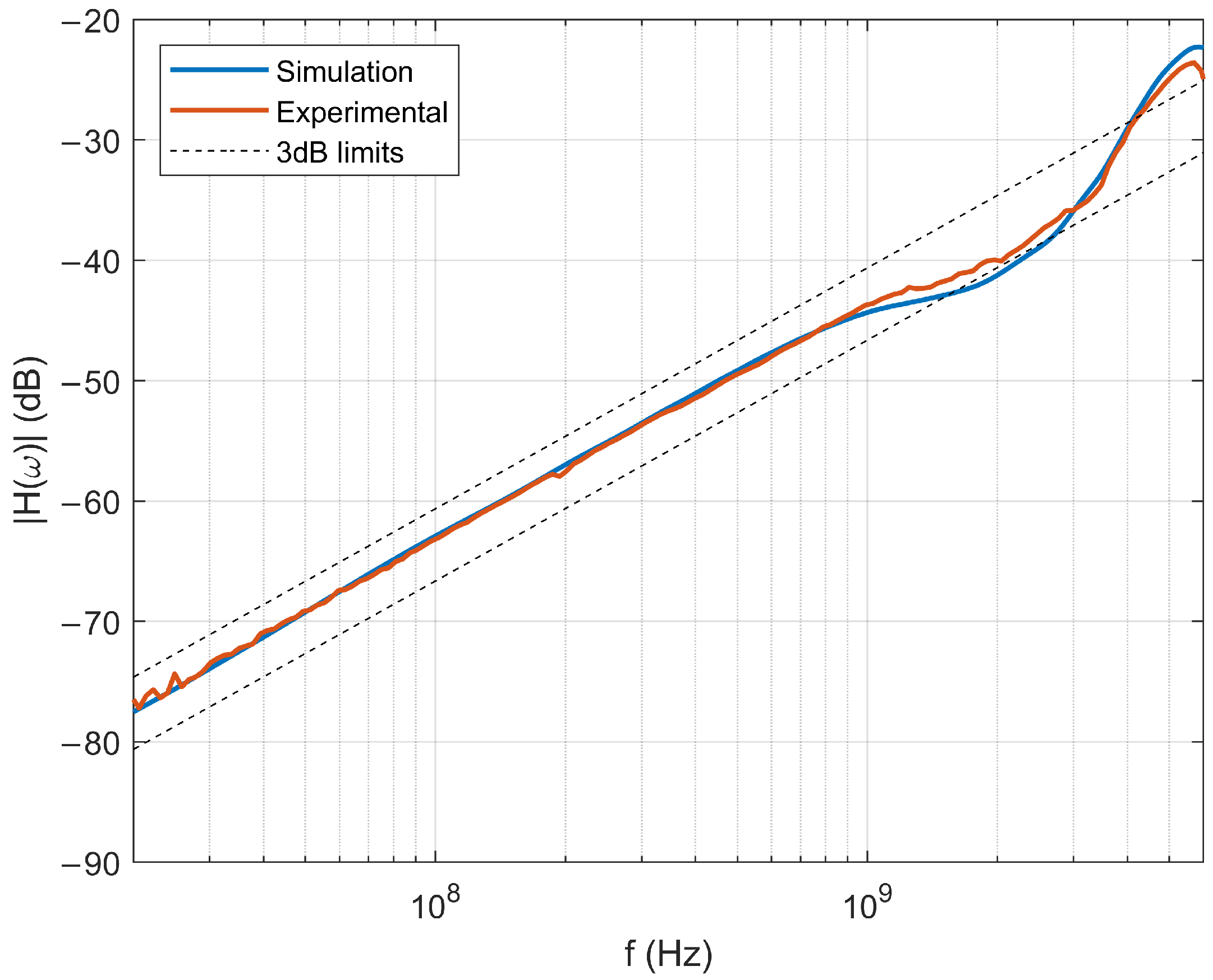
The optimized sensor was fabricated and characterized using the same instrumentation and methodology described in
Section 3.1. The frequency response of the sensor is shown in
Figure 8. Notably, although the simulation’s maximum frequency was 10 GHz, the experimental data closely matches the simulated response up to approximately 6 GHz. Beyond this range, all D-dot designs cease to act in their derivative mode, rendering frequencies above this threshold outside the scope of interest.
The next section will present a comparison between the frequency response of the optimized sensors and the planar D-dots proposed in [
10], while also exploring a frequency-domain-based definition of bandwidth for these sensors and examining their time transient response in relation to their ability to sense nanosecond and sub-nanosecond pulses.
4. Results and Discussion
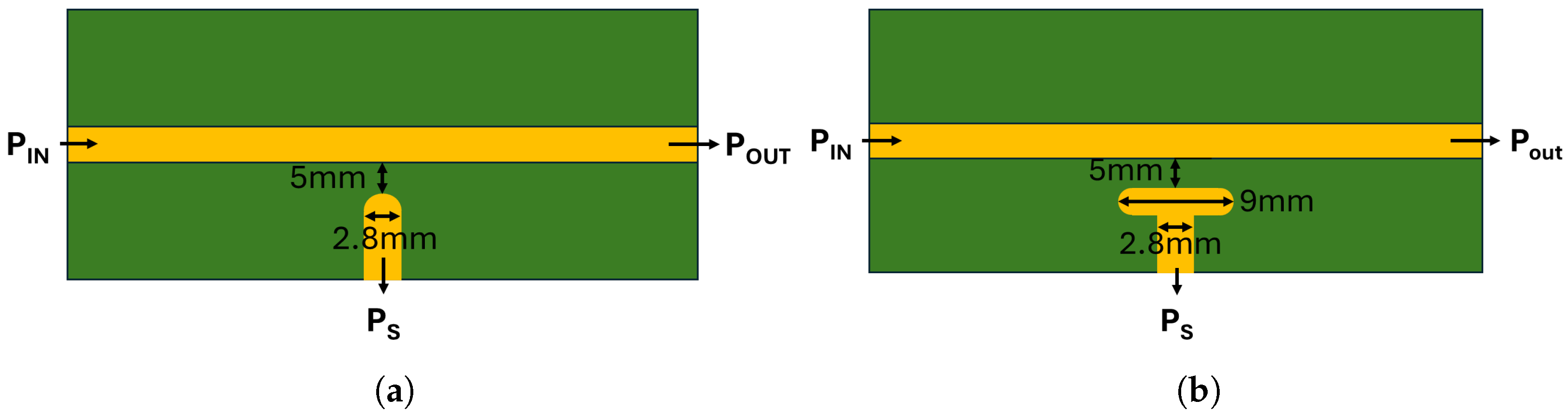
This section presents the results of frequency- and time-domain measurements to determine the experimental response of the optimized sensors. Additionally, two planar D-dots identical to those proposed in [
10] were fabricated and tested to highlight the bandwidth improvement in the new designs. These sensors, originally called “Padded” and “Non-padded” in [
10], will retain the same designations here for consistency, and their designs are presented in
Figure 9. The set-off distance was maintained at
mm, and both sensors were fabricated on the same TMM4 substrate as the optimized designs.
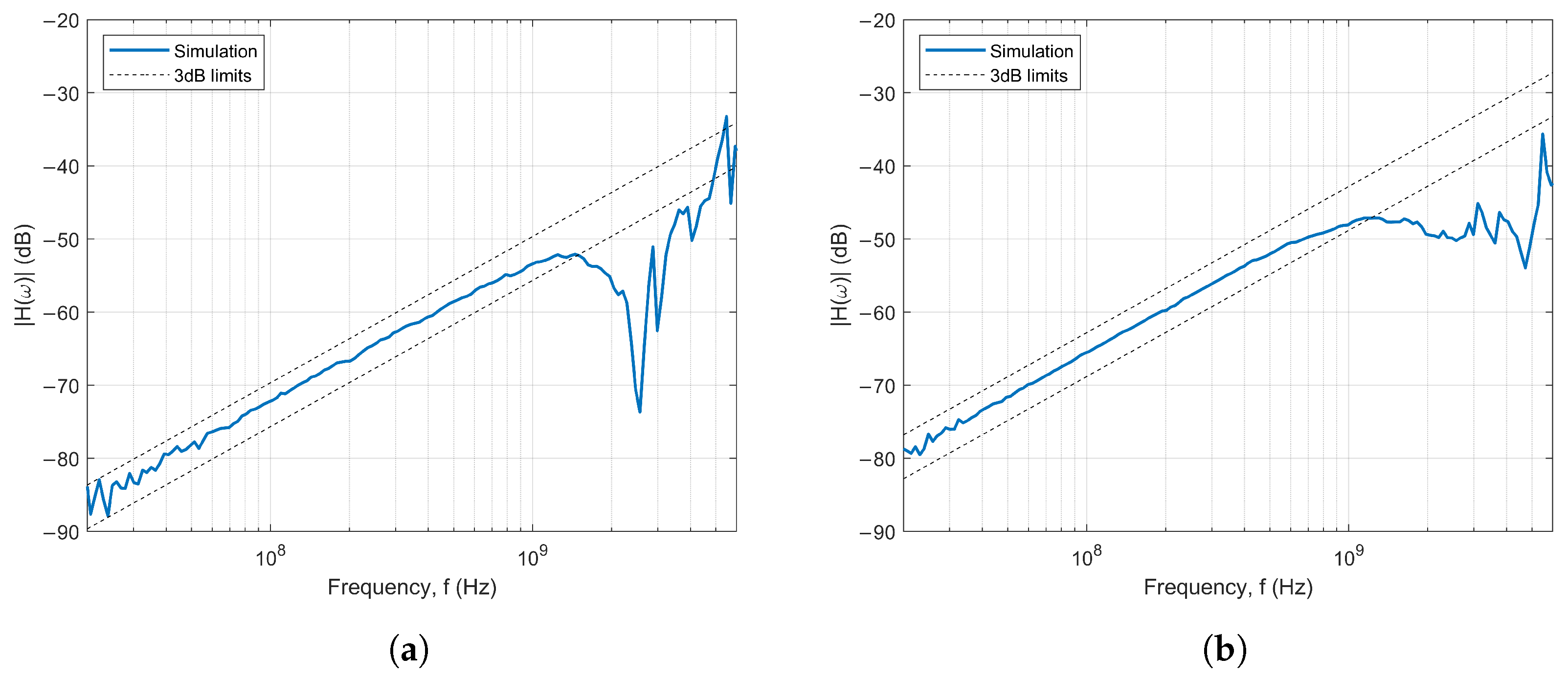
The frequency responses of the “Non-padded” and “Padded” sensors exhibited a clear degradation in the derivative behavior for frequencies above 1.2 GHz, along with a resonance, commonly associated with stray inductance and signal travel time along the surface of the sensor’s head [
9] as depicted in
Figure 10.
While the primary interest in D-dots is their ability to measure fast signal transients, it is also convenient to have a way to compare them in the frequency domain. To facilitate this comparison, a 3 dB limit is defined as the point where the experimental response deviates by more than ±3 dB from the expected response of an ideal derivative, also known as the low-frequency approximation (LFA) of the D-dot. Therefore, the 3 dB limit can be used to estimate at which frequencies a D-dot stops acting in its “derivative mode” and transitions into the “self-integrating mode”, which correlates with the sensor’s bandwidth [
13,
15,
27].
Figure 11 shows an overlay of the frequency response of all D-dots evaluated in this study, with the 3 dB limits marked to indicate the estimated bandwidth of each sensor. Not only is the bandwidth extended in the proposed designs, but their gain is also increased, which is reflected by the sensor’s responsivity (
).
The responsivity of each sensor was estimated in the LFA using Equation (
3). The results can be found in
Table 1, showing that the highest bandwidth was achieved by the T-shape sensor, while the Spline sensor exhibited the highest responsivity.
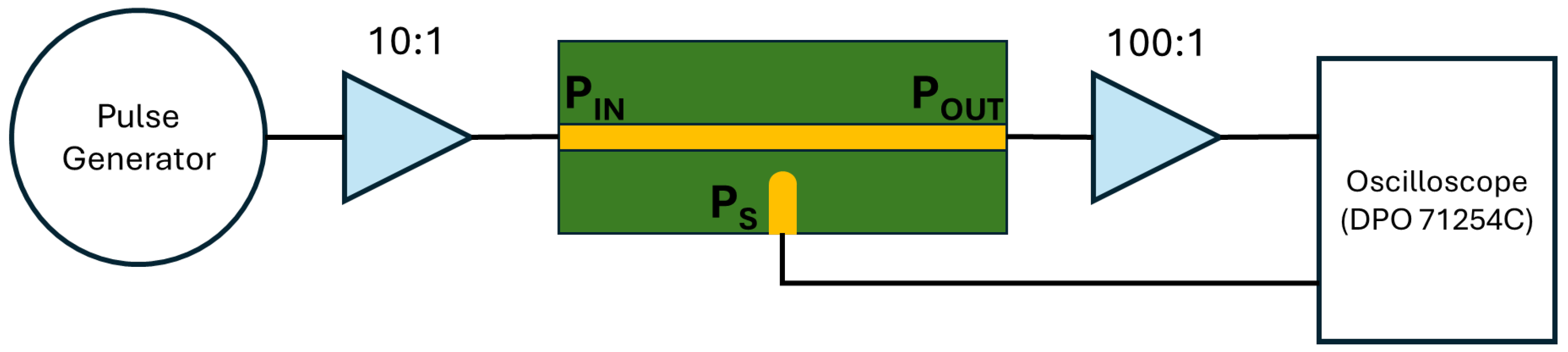
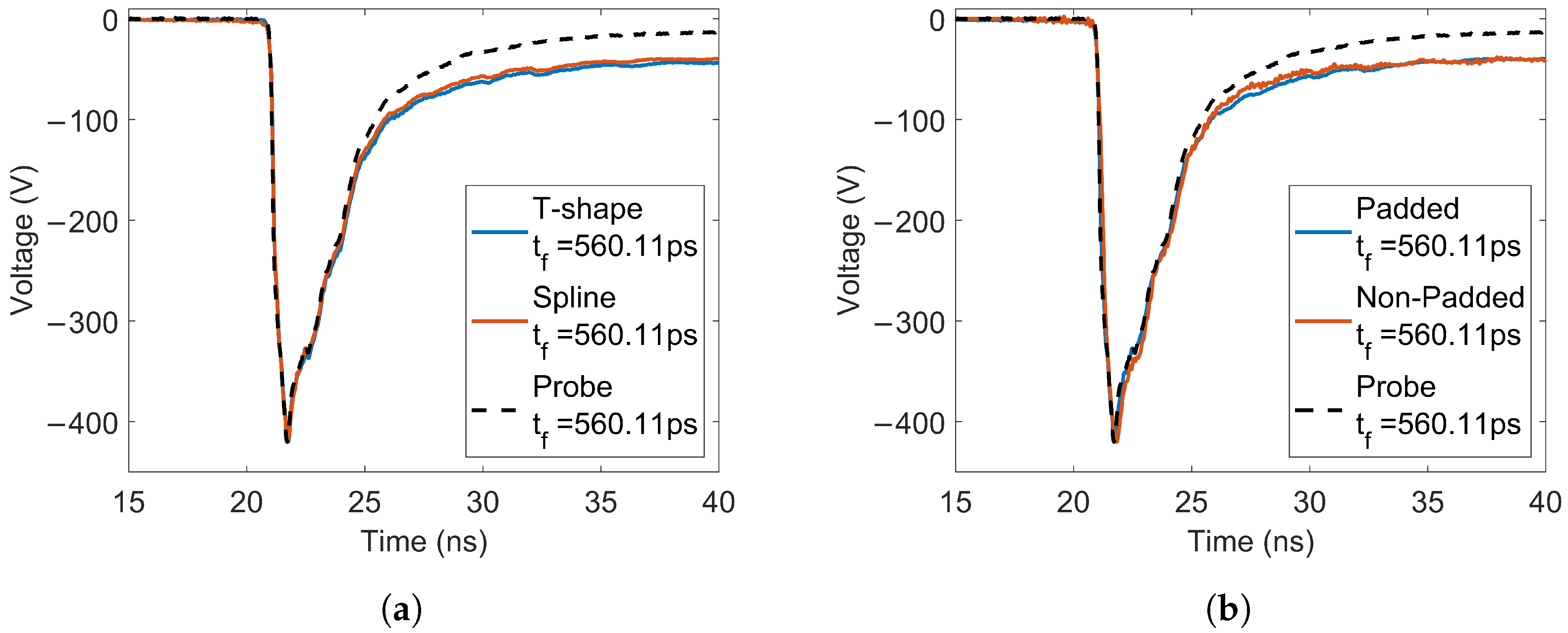
4.1. Time-Domain Characterization Using High-Voltage Sub-Nanosecond Pulse Generator
To evaluate the ability of the proposed sensors to measure fast transient signals, a series of time-domain tests were conducted by applying sub-nanosecond rise-time pulses into the microstrip line arrangement and recording the sensors’ response. The results were numerically integrated and compared with the measurements from a 12.5 GHz Oscilloscope DPO 71254C (Tektronix, Berfordshire, OR, USA) ) connected to port
. The pulses with a peak voltage of −4.2 kV, an approximate rise-time of 560 ps (
= −840 V/ns,
625 MHz), and ∼3 ns FWHM were produced by a Grant Applied Physics pulse generator (San Francisco, CA, USA), which was connected to port
through a 10:1 high-bandwidth attenuator; the signal then circulated through the microstrip line that was also connected to the oscilloscope using another 100:1 high-bandwidth attenuator string. Due to inherent attenuation of the D-dot, no intermediate attenuation was necessary between the port
and the oscilloscope as seen in
Figure 12.
Figure 13 shows the integrated signals from both proposed D-dots and the designs from [
10], as well as the output of the microstrip line (Probe). All designs successfully captured the fast transient during the falling edge of the signal, consistent with the estimated bandwidth shown in
Figure 11. However, the after-pulse section exhibits a substantial offset, which has been previously attributed to factors such as current imbalance in the measurement path, charge accumulation, or a resistive path between the sensor head and the power trace [
28]. Other studies have concluded that this behavior can be mitigated by applying advanced signal processing and numerical integration techniques [
28]; nonetheless, these solutions are beyond the scope of this document and will not be explored in detail.
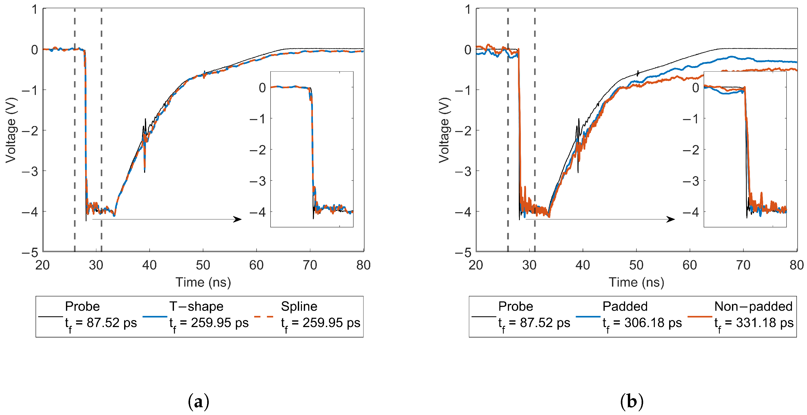
4.2. Time-Domain Characterization Using Low-Voltage Picosecond Pulse Generator
To further explore the capabilities of the optimized D-dots, the sensors were additionally tested using a −4 V pulse with a leading-edge rise time of ∼18.75 ps (
= −213 V/ns,
19 GHz) generated by a 4015C pulse generator (Picosecond Labs, Boulder, CO, USA). The experimental setup was identical to that shown in
Figure 12, except that no attenuating elements were used. It is important to mention that due to the limitations of the equipment, the signals appear to be slower than they truly are; nonetheless, the front-edge of the testing pulse is sufficiently fast to strain the sensors’ bandwidth, allowing the characterization of the proposed designs under picosecond transient conditions.
Figure 14 illustrates the superior performance of the proposed D-dots reproducing the fast transient features of the input signal while minimizing the remaining offset at the tail of the pulse. Although the 3 dB limit of the optimized designs suggests a minimum rise-time of 81 ps for the T-shape sensor and 194 ps for the Spline sensor, the observed rise-times of the recovered signals appear to be longer. This discrepancy arises from small perturbations during the leading edge of the recovered signal that cause the 10–90 rise-time to be longer than expected; that said, it is important to note that the slew rate of both original and recovered signals achieved the same maximum
, evidencing the sensor speed.
While a definitive explanation for the perturbations is not available, it is theorized that high-order harmonics with wavelengths comparable to the sensor head may induce traveling waves along it, resulting in the observed oscillations. In the case of the picosecond pulse generator, the manufacturer specifies a minimum rise-time of 18.8 ps, whereas an 87.5 ps value was measured. These values imply a 3 dB pulse bandwidth of at least 4 GHz, corresponding to spectral components with wavelengths near 2 cm, the same order as the sensor head length. At such frequencies, traveling waves are expected to propagate along the sensor head and reflect off its ends, causing transient-time ripples on the waveform rising edge.
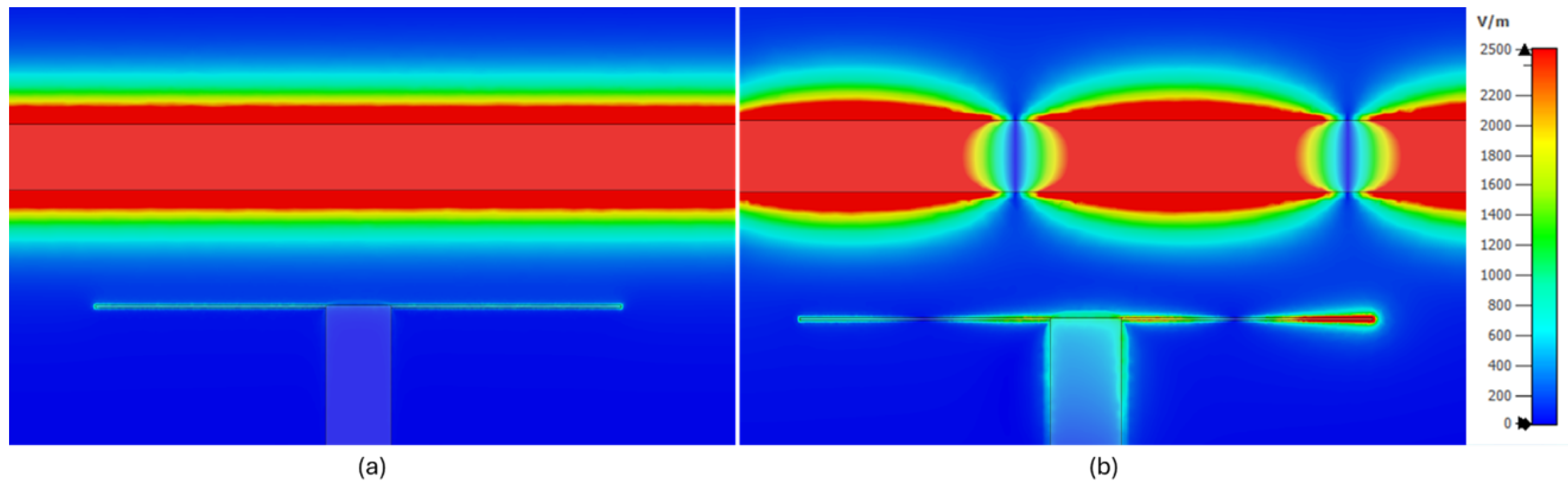
This hypothesis is supported by EM simulations (see
Figure 15 and
Figure 16), which show that for low frequencies, the electric field is homogeneously induced along the sensor’s head for both optimized geometries. However, as the sensing signal frequency increases, traveling waves appear and move along the sensor head.
Due to its capacitive nature, the frequency response of these planar sensors is influenced by both geometrical variations and the substrate’s relative permittivity according to the analytical expressions provided in [
11]. Consequently, each design must be matched to a specific substrate and a minimum manufacturing accuracy to maintain performance consistency.
5. Conclusions
This work demonstrated that the bandwidth of planar voltage sensors can be extended by using parametric optimization, suggesting that the inverse relationship between gain and bandwidth is not direct. In fact, the results indicate that bandwidth can be enhanced without significantly compromising gain or responsivity to limits not yet established, which encourages the exploration of different sensor geometries through more sophisticated methods such as topology optimization [
29]. The promising performance of planar voltage sensors along with their simple fabrication process makes them an interesting alternative to resistive probes, potentially improving the sensing capabilities for high-power pulse measurements in PCB-based systems and beyond. It is expected that the proposed framework enables the design of custom, PCB-integrated sensors to support the development of sensing solutions tailored to specific application requirements and fabrication constrains. This approach is particularly relevant to emerging solid-state fast-switching systems such as pulsed power generators and switching power supplies, where compactness and adaptability are essential.
Future efforts will aim to study the minimum hold-off voltage of planar sensors and its interrelation with the materials and manufacturing techniques used in their fabrication, as well as reducing after-pulse offset and undesired ringing on the front edge of the recovered signal.


