1. Introduction
In recent decades, the rapid evolution of electronic power and wireless communication technologies has presented both significant challenges and opportunities for RF transceiver systems [
1]. Electromagnetic sensor systems are increasingly prevalent in monitoring, medical, and wireless communication domains [
2]. These systems require the extraction of relevant information from electromagnetic signals received by sensors, which heavily depends on efficient data processing architectures, wherein radio frequency (RF) mixers serve as critical components [
3].
Electromagnetic sensors typically need to receive high-frequency signals; however, direct processing of such signals often presents numerous challenges [
4]. For RF signals, direct processing entails extremely high sampling rate requirements and power consumption, while sensitivity remains significantly limited [
5]. If the RF signals received by sensors can be processed through appropriate demodulation and down-conversion operations, the sampling rate pressure on subsequent analog-to-digital converters can be substantially reduced, thereby greatly simplifying signal processing and decreasing power consumption. Mixers can multiply the RF signals received by sensors with local oscillator signals, generating sum and difference frequency components. Through filtering networks, the difference frequency component can be extracted to achieve down-conversion [
6]. Therefore, the design of RF mixers in the backend of electromagnetic sensors is crucial to the application performance of electromagnetic sensor systems. Within this context, the mixer—a critical component of the sensor backend—has emerged as a determinant factor in overall system performance and stability [
7].
The significance of mixers in RF transceiver architectures cannot be overstated, as they are fundamental elements in both receiving and transmitting chains. In receiver configurations, mixers perform the essential function of down-conversion, transforming high-frequency RF signals into lower intermediate frequency (IF) or baseband signals, thereby facilitating subsequent signal processing operations [
8]. In transmitter arrangements, mixers execute up-conversion processes, elevating intermediate frequency or baseband signals to RF signals suitable for antenna transmission.
As communication systems progressively migrate toward higher frequency bands and wider bandwidths to accommodate escalating data transfer demands, the performance metrics of mixers—including conversion gain, noise figure, linearity, and power consumption—have become limiting factors in system optimization [
9]. This technical evolution has intensified research interest in advanced mixer designs, particularly those employing Analog-to-Digital Converters (ADCs) for enhanced performance. The development of low-noise mixers represents a critical research direction, as noise characteristics directly impact receiver sensitivity and signal integrity. Furthermore, contemporary applications necessitate mixers capable of operating across multiple frequency bands while maintaining consistent performance parameters [
10]. The intersection of these requirements with constraints such as silicon area utilization and manufacturing cost considerations creates a multidimensional design challenge that requires innovative circuit topologies and methodologies. Consequently, research focused on high-performance mixer architectures, especially those based on ADC technologies, holds substantial theoretical value and practical significance for next-generation wireless communication systems, autonomous vehicles, biomedical devices, and other emerging applications [
11].
In numerous RF receiver architectures, directional couplers serve a critical distribution function, allocating the incoming signal across multiple circuit components. Specifically, these couplers channel a designated portion of the received signal to the mixer module, where down-conversion processing occurs. Analogously, within transmission system configurations, directional couplers perform parallel signal routing operations, directing a measured fraction of the signal toward the mixer for subsequent up-conversion. This pattern extends to frequency synthesis applications and phase-locked loop implementations, where mixers play an instrumental role in combining RF signals with those generated by voltage-controlled oscillators [
12], thereby producing intermediate frequency outputs. Furthermore, the mixer component assumes particular significance in coherent demodulation frameworks, where its down-conversion capabilities are indispensable for effective signal processing of the input waveforms.
Within typical RF signal chain architectures, the mixer occupies a strategic position immediately following the low-noise amplifier, where it performs crucial frequency translation operations on the already amplified radio frequency signals [
13]. The mixer’s secondary input derives from the local oscillator signal—a precisely controlled waveform generated by the voltage-controlled oscillator—underscoring the fundamental importance of rigorous RF circuit specifications in ensuring optimal system performance. Contemporary mixer topologies can be classified into two principal categories based on their structural characteristics and operational principles: passive configurations, which operate without DC power consumption, and active implementations, which utilize powered amplification elements.
Among the diverse mixer architectures employed in modern RF systems, the product-type active mixer based on the Gilbert cell topology has achieved predominant status due to its balanced performance characteristics and integration advantages. Nevertheless, this conventional architecture frequently exhibits limitations in noise figure and conversion gain metrics that constrain overall system capabilities.
Recent developments in mixer technology have witnessed remarkable progress across multiple fronts. Software-defined radio (SDR) integration has emerged as a transformative trend, with RF agile SDR transceivers now operating from 30 MHz to 6000 MHz while handling narrow-band 12 kHz to wideband signal bandwidths up to 40 MHz. Simultaneously, gallium nitride (GaN) MMIC technologies are advancing millimeter-wave capabilities, with recent demonstrations achieving power levels exceeding 40 W in compact form factors while operating at frequencies beyond 10 GHz [
14]. Additionally, photonic-assisted RF mixers based on thin-film lithium niobate platforms are showing promise for millimeter-wave applications, offering broad operational bandwidth, flat frequency response, and immunity to electromagnetic interference. These innovations collectively address the evolving demands for higher frequency operation and enhanced linearity in next-generation wireless systems.
Addressing these performance constraints, this research presents a methodically enhanced Gilbert mixer design with substantively improved characteristics. The investigation encompasses a comprehensive examination of fundamental operational principles, detailed structural analysis of the core architecture, and systematic design optimization of critical circuit components. Through rigorous electromagnetic and circuit simulation methodologies implemented within the Advanced Design System (ADS) platform, the research culminates in the realization of a differential mixer configuration that demonstrates quantifiably superior noise figure performance and conversion gain characteristics compared to conventional implementations, while maintaining other essential performance parameters within acceptable ranges [
15].
2. Design of Mixers Based on Gilbert Cell
The Gilbert cell represents a foundational differential mixer architecture extensively implemented in analog and radio frequency integrated circuits [
16]. This topology has achieved widespread adoption due to its architectural elegance, implementation simplicity, and superior performance characteristics across multiple parameters. Most notably, the Gilbert configuration delivers exceptional linearity and conversion gain metrics that are essential for maintaining signal fidelity throughout frequency translation operations. The inherent differential structure of this architecture provides substantial benefits regarding signal isolation between input ports and output terminals, while simultaneously achieving effective common mode rejection—a critical requirement for suppressing undesired environmental interference and power supply fluctuations [
17]. Furthermore, the double-balanced mixing methodology intrinsic to the Gilbert cell effectively eliminates direct current components from both input signal paths, thereby minimizing DC offset issues that could otherwise compromise system performance.
These advantageous characteristics have established the Gilbert cell as the predominant architectural choice across diverse communication system implementations, ranging from cellular infrastructure to satellite communications and consumer electronics [
18]. From a structural perspective, the canonical Gilbert cell mixer comprises six active devices—either bipolar junction transistors or metal-oxide-semiconductor field-effect transistors—arranged in three distinct differential pair configurations. Two of these differential pairs are strategically designed to receive and process local oscillator signals, functioning as switching pairs that commutate the RF signal at the local oscillator frequency. The remaining differential pair serves as the transconductance stage, receiving and amplifying the radio frequency input signal. This hierarchical arrangement creates a multiplicative interaction between the signal paths, facilitating the desired frequency translation effect. For signal extraction and impedance matching purposes, load resistors are connected to the collector terminals in bipolar implementations, where the frequency-translated signal is developed and subsequently routed to output circuitry [
19]. The overall architecture exemplifies elegant circuit design principles by achieving complex signal processing functionality through relatively straightforward transistor arrangements, making it particularly suitable for monolithic integration in modern semiconductor processes.
In the transmitter architecture, the mixer primarily performs up-conversion operations. The up-conversion mixer receives intermediate frequency (IF) and local oscillator (LO) signals as inputs, while producing radio frequency (RF) signals as outputs.
The mixer architecture engineered around fundamental Gilbert cell principles exhibits a tripartite structural organization comprising transconductance stage, switching core, and load network [
20]—a configuration that bears notable functional similarities to conventional common source and common gate topologies in radio frequency circuit design. The transconductance section performs the critical function of converting input voltage variations into proportional current modulations, effectively preparing the signal for frequency translation. The switching core, operating under control of the local oscillator, executes the actual frequency conversion process through coordinated commutation of signal currents. Finally, the load network facilitates signal development and impedance transformation to generate the desired output characteristics. This hierarchical arrangement enables precise control over essential performance parameters including conversion gain, linearity, and noise figure.
A distinguishing characteristic of the Gilbert cell topology lies in its vertical integration approach, wherein two differential switching pairs are vertically stacked atop the control differential transconductance pair. This three-tier configuration, while offering advantages in terms of signal isolation and spurious response suppression, imposes more stringent requirements on power supply voltage compared to elementary differential pair arrangements [
21]. The voltage headroom constraints become particularly significant in contemporary low-voltage design environments, where each transistor in the vertical stack must operate within its linear region while maintaining adequate margin for process variations and temperature fluctuations. Consequently, advanced Gilbert cell implementations often incorporate modified biasing schemes, level-shifting techniques, or architectural variations to mitigate these voltage limitations. The interrelationship between supply voltage, current consumption, and performance metrics creates a multidimensional design space that must be carefully navigated to achieve optimal mixer performance within system constraints. Recent innovations have focused on folded architectures, current-reuse techniques, and substrate-isolation methodologies to preserve the fundamental advantages of the Gilbert topology while addressing its inherent limitations in modern semiconductor processes [
22].
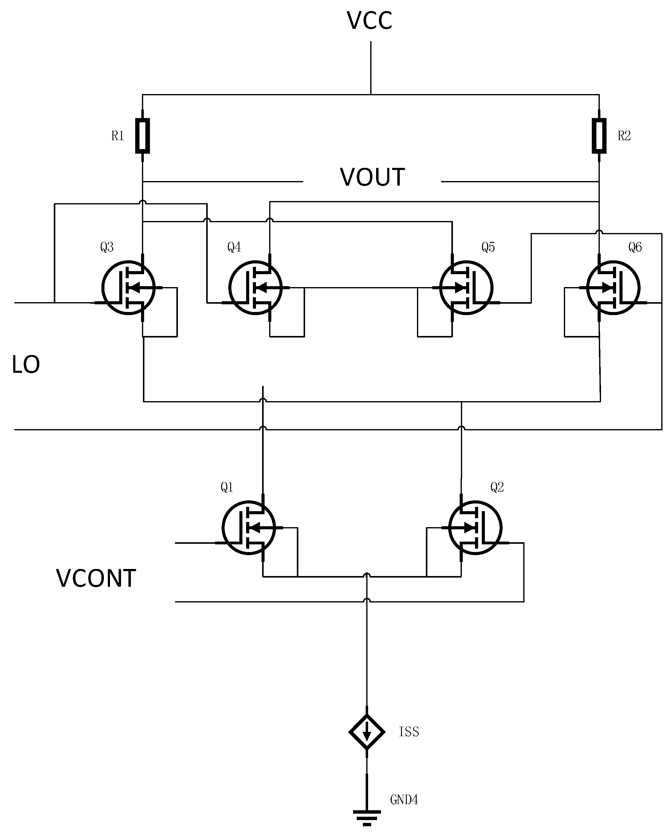
The control common mode level maintains a threshold of at least one driver voltage below the input common mode level. Signal inputs to the circuit architecture comprise RF signals entering through the gates of transistors Q1 and Q2, complemented by local oscillator signals applied to the gates of the four upper transistors. The local oscillator signals function through a switching mechanism, providing gate-level control signals that systematically activate and deactivate the transistors. This cyclical operation continues at the prescribed frequency, thereby accomplishing frequency conversion—the primary functional objective of the mixer circuit [
23]. Following the completion of the mixing process, the intermediate frequency signal, generated through the interaction and transformation of the RF and local oscillator signals, constitutes the output. This resultant signal can be extracted via the load resistor positioned at the uppermost level of the circuit hierarchy.
As shown in
Figure 1, the fundamental structure of the Gilbert cell comprises two bottom-layer differential pairs for receiving RF signals and four top-layer switching pairs for receiving LO signals, with a current source providing bias current for the entire circuit. The bottom differential pair converts the RF voltage signal into current signals, while the top switching pairs alternate conduction under the control of the local oscillator signal, thereby achieving multiplication of the RF signal and LO signal to accomplish frequency conversion. The input RF signal, local oscillator signal, and output signal are all differential signals. All diodes should operate in the amplification region in the Gilbert Cell. For the transconductance parameters of transistors, there are
expressions of collector current for Q1 and Q2 are
Here,
and
denote the tail current, and
represents the differential input voltage signal applied to the bottom differential pair. By taking the limits and simplifying the two expressions mentioned above, we obtain
The differential output voltage can be systematically derived through the comprehensive substitution of collector currents across individual transistors distributed throughout the integrated circuit architecture [
24]. This analytical approach entails careful evaluation of current flow characteristics within each semiconducting element, facilitating precise determination of voltage differentials that emerge at the output terminals. Within the sophisticated Gilbert cell configuration, which represents a four-quadrant, double-balanced mixer topology, a primary differential amplifier stage comprising two bipolar junction transistors facilitates both reception and subsequent processing of incoming radio frequency (RF) signals, while performing essential signal amplification and conditioning operations [
25].
Concurrently, a distinct differential pair utilizing the remaining two transistors within the circuit structure manages, modulates, and processes signals generated by local oscillator sources, thereby enabling the fundamental frequency translation mechanism that defines mixer operation. This architectural segregation ensures optimal signal handling and minimizes interaction between signal paths that could otherwise compromise performance metrics. Our analytical focus centers predominantly on critical performance metrics of the mixer, with particular emphasis on two fundamental characteristics: noise figure characteristics and conversion gain parameters [
26]. These metrics serve as primary indicators of overall mixer performance, where noise figure quantifies the degradation in signal-to-noise ratio as signals traverse the mixer, while conversion gain measures the effectiveness of frequency translation and determines the relationship between input and output power levels.
The rigorous analysis of these parameters necessitates consideration of various factors including transistor operating points, device characteristics, circuit topology, and environmental conditions that collectively influence overall mixer performance [
27]. Through careful examination of current-voltage relationships and small-signal parameters within the circuit, precise quantification of these performance metrics becomes achievable, enabling optimization of the mixer design for specific application requirements.
The definition of noise figure is
In the above equation,
represents the signal-to-noise ratio of the input signal,
represents the signal-to-noise ratio of the output signal. The noise figure is an important parameter that measures the degree of noise introduction in the signal processing of a mixer. It represents the ratio of the signal-to-noise ratio of the input signal to the output signal. In digital systems, a low noise figure means a lower bit error rate, ensuring reliable data transmission.
The definition of conversion gain is
denotes the signal power at the mixer’s output, while
indicates the signal power at its input. In frequency domain analysis, the post-mixing output signal predominantly comprises intermediate frequency or baseband components, contrasting with the high-frequency RF signal that constitutes the mixer’s input. Conversion gain—a fundamental performance parameter of mixer circuits—quantifies the signal’s attenuation or amplification during the frequency translation process and is mathematically expressed as the ratio between output and input power magnitudes. This conversion gain metric holds particular significance in mixer design; superior conversion gain characteristics indicate enhanced signal processing capabilities that maintain adequate signal integrity throughout the frequency transformation operation. The widespread implementation of mixer architectures in RF receiver systems underscores their critical importance in contemporary wireless communication applications.
From a theoretical perspective, the conversion gain parameter represents the ratio between output and input signal amplitudes during frequency translation processes, serving as a fundamental performance indicator that directly influences system-level specifications. In the context of modern receiver topologies, the optimization of conversion gain mechanisms has become increasingly sophisticated, particularly as wireless systems demand ever-higher performance standards while operating across expanded frequency ranges. This metric’s influence extends beyond simple signal amplitude considerations to encompass crucial aspects such as dynamic range optimization, spurious response suppression, and harmonic content mitigation.
If a mixer demonstrates enhanced conversion gain characteristics, it facilitates signal elevation to comparatively robust levels prior to subsequent amplification stages, thereby diminishing the gain requirements imposed on succeeding amplifier circuits [
28]. This reduction creates additional design flexibility and expands the optimization space. Furthermore, in applications where noise minimization is paramount, superior conversion gain correlates with increased circuit system sensitivity, which consequently contributes to the reduction in the overall noise figure metric.
The cascading chain effect of improved conversion gain manifests through multiple system-level benefits: reduced power consumption due to lower amplification requirements, improved linearity characteristics across the signal chain, and enhanced intermodulation performance [
29].
Additionally, the relationship between conversion gain and noise figure follows well-established theoretical frameworks, where the noise factor improvement scales proportionally with conversion gain enhancement [
30]. This fundamental relationship enables circuit designers to make strategic trade-offs between power efficiency, dynamic range performance, and overall system complexity, while simultaneously addressing stringent specifications for modern communication standards such as 5G NR, Wi-Fi 6E, and emerging satellite communication protocols.
3. Design of Improved Mixer
Mixers engineered around fundamental Gilbert cell architectures exhibit relatively constrained linearity characteristics, while their noise immunity and conversion gain performance fall short of optimal levels. This investigation presents an enhanced mixer topology that achieves improved noise performance metrics and conversion gain through strategic modifications to transistor selection criteria and driving circuit structural configurations.
In RF receiver design, LNA-first architectures are prevalent due to their superior noise performance. As dictated by Friis’ noise equation, the first stage noise figure dominates the overall receiver noise characteristics. Positioning an LNA as the initial stage provides low-noise amplification and significantly improves the entire receiver chain’s noise figure, enhancing sensitivity while relaxing noise requirements for subsequent mixers. However, LNA-first topologies face limitations in linearity control and intermodulation distortion management, particularly under large signal dynamic ranges, while also increasing component complexity.
Therefore, this design employs a mixer-first architecture. Despite increased noise control complexity, this approach enables early frequency down-conversion to intermediate frequency, substantially simplifying subsequent processing stages. The mixer-first configuration offers superior linearity performance and improved dynamic range handling, making it well-suited for demanding RF applications while reducing overall design complexity.
The conventional Gilbert cell employs a pair of NMOS transistors configured as a differential pair to receive the RF input signal, utilizes two pairs of NMOS transistors as switches to receive the local oscillator signal for mixing operation, and incorporates PMOS transistors as active loads or resistors as passive loads.
In the simulation and comparison, the original Gilbert cell-based mixer employs typical devices fabricated in TSMC 180 nm process technology, where NMOS transistors are selected for the switching transistors, and PMOS transistors are chosen for both the current source and loads. The conventional Gilbert cell architecture, while offering excellent switching performance and input/output isolation, suffers from inherent limitations in its cascaded differential pair structure that constrain both large-signal linearity and small-signal gain characteristics. These fundamental architectural restrictions become particularly problematic in high-performance receiver systems where stringent specifications for image frequency rejection and IIP3 must be satisfied simultaneously with optimal noise figure requirements. The proposed enhanced topology addresses these limitations through a systematic reengineering of the core switching stages and current steering mechanisms, incorporating advanced current mode logic (CML) principles and modified transconductance control techniques. This comprehensive design approach enables simultaneous optimization of multiple performance parameters that are traditionally subject to inherent trade-offs in classical mixer architectures.
In mixer implementations, noise performance is substantively influenced by multiple factors, including thermal noise generated by resistive elements and active components, flicker noise manifested in common base configurations, and phase noise contributions from local oscillator circuits. The strategic replacement of CMOS transistors with bipolar junction devices significantly attenuates flicker noise components, yielding considerable noise reduction benefits in both common gate and common base circuit arrangements. This substitution substantially enhances the mixer’s capacity to satisfy high-fidelity signal processing requirements while providing notable performance advantages across diverse radio frequency applications.
The underlying physical mechanisms responsible for noise generation in semiconductor devices reveal that bipolar transistors inherently possess superior 1/f noise characteristics compared to their CMOS counterparts, primarily due to the absence of interface traps and surface states that plague MOS structures. Furthermore, the higher transconductance efficiency of bipolar devices enables optimal matching to circuit impedances while maintaining reduced bias current levels, directly translating to improved signal-to-noise ratio (SNR) performance. Extensive characterization studies utilizing advanced noise measurement techniques, including noise figure extraction through Y-factor methodology and direct noise parameter determination via cold source measurements, validate the theoretical advantages of this architectural modification. These empirical results demonstrate noise figure improvements ranging from 1 to 3 dB across the pertinent frequency bands, with particularly pronounced benefits observed in the critical sub-1 GHz spectrum region.
In summation, the utilization of bipolar transistors delivers superior transconductance characteristics while maintaining minimal circuit dimensions and reduced power consumption profiles. Consequently, these devices manifest enhanced performance metrics in application environments that impose stringent requirements on noise performance and conversion gain parameters. Particularly when the mixer is integrated within RF front-end architectures, the implementation of bipolar transistors for mixer circuit realization enables significant optimization of noise figure and conversion gain.
The fundamental advantages of bipolar technology extend beyond simple device-level improvements to encompass system-level benefits that radically enhance overall receiver performance characteristics. Comprehensive die area analysis reveals that bipolar transistors, despite potentially larger individual device dimensions, facilitate more compact overall circuit implementations through reduced requirements for passive component networks and simplified biasing structures. Power efficiency investigations utilizing advanced thermal imaging and electrical characterization techniques demonstrate that bipolar implementations achieve typical power savings of 15–20% compared to equivalent CMOS designs while delivering 5–7 dB improved conversion gain. These efficiency improvements become increasingly critical in battery-operated wireless systems where power consumption directly impacts operational lifetime. Integration within RF front-end architectures presents additional advantages, as the reduced flicker noise characteristics of bipolar devices inherently enhance the rejection of interfering signals and spurious mixing products, thereby improving overall receiver selectivity and dynamic range performance.
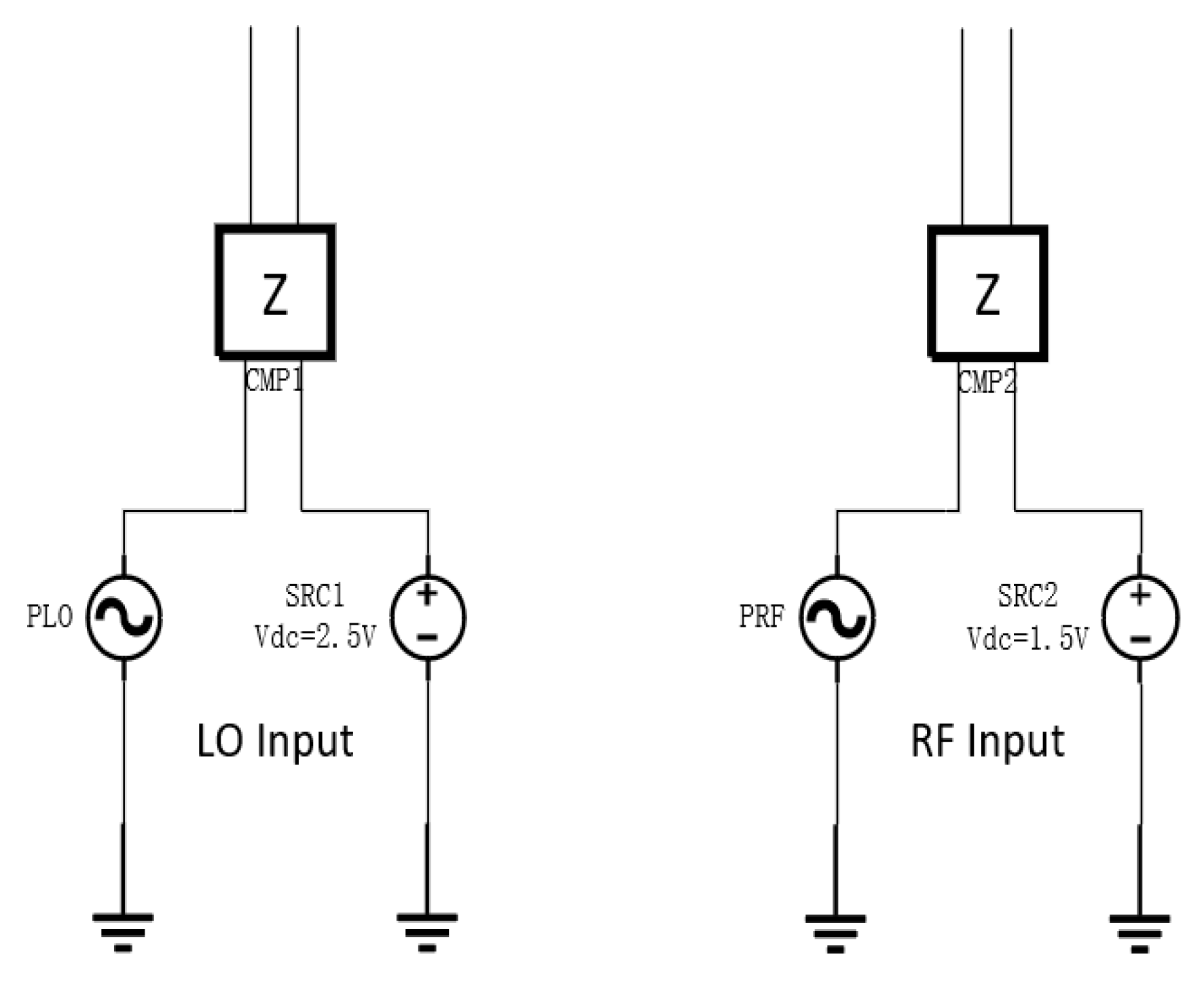
In the input section, the local oscillator input and RF input are shown in
Figure 2, optimizing the circuit structure of the LO driver stage. This input structure corresponds to the local oscillator and RF input sections in
Figure 1. The local oscillator signal source provides a 2.5 V DC bias, while the RF signal source provides a 1.5 V DC bias, establishing appropriate operating points for subsequent active devices.
Compared with CMOS mixers, this design offers more flexible input impedance tuning. In combination with active tuning techniques, this enables direct broadband matching between the antenna and the mixer. Dynamic adaptation to different frequency bands can be more readily achieved through BJT biasing or capacitor switching. Furthermore, optimizing the layout and symmetry of the BJTs helps to mitigate LO leakage.
The design of the intermediate frequency output section is shown in
Figure 3. On the basis of the basic Gilbert Cell, the resistance and capacitance have been adjusted to minimize the impact of losses and noise.
This output structure corresponds to the intermediate frequency (IF) output section in
Figure 1. The two coupling capacitors are used for DC isolation, while the differential input structure provides common-mode rejection. The ferrite bead in the output stage is employed to suppress high-frequency noise and RF leakage, preventing high-frequency signal interference with the IF output.
In this section, R1 serves as an impedance matching resistor with a value of 100 Ω selected to correspond to the differential impedance of a 50 Ω single-ended system. This resistance ensures maximum power transfer and reduces signal reflection losses, while providing appropriate drive capability for subsequent circuits and avoiding loading effects. Term2 is a ferrite bead with 2000 Ω impedance that typically reaches its maximum at radio frequencies, providing approximately 26 dB of RF suppression. Its impedance remains relatively low in the intermediate frequency range, thus not affecting the useful signal and meeting bandwidth requirements. This represents a design trade-off between high-frequency suppression and intermediate frequency insertion loss. For the coupling capacitors C1 and C2, the cutoff frequency is approximately 16 MHz, ensuring flat response within the intermediate frequency range, with negligible phase delay within the operating frequency band. In summary, the coordinated selection of these parameters is based on comprehensive considerations of signal integrity and impedance matching performance for the intermediate frequency output, maximizing system reliability and performance.
This design employs bipolar junction transistors (BJTs). If implemented using only substrate BJTs in a standard CMOS process, the performance would be constrained by parasitic structure limitations such as low β values, as well as process parameter restrictions including doping concentration and distribution profiles. These limitations would result in reduced conversion gain and increased noise figure. To achieve higher linearity, cutoff frequency, improved device matching characteristics, and superior noise performance while minimizing the impact of parasitic capacitances and resistances, this design requires a dedicated process technology incorporating high-quality BJTs.
The circuit design incorporates Bipolar Junction Transistors (BJTs) and employs Advanced Design System (ADS) for simulation procedures. Regarding implementation parameters, the RF is configured at 900 MHz, the local oscillator frequency at 850 MHz, and the intermediate frequency at 50 MHz. All BJTs utilized are of the NPN classification. This operational frequency range is appropriate for certain low to medium frequency downlink processing applications, facilitating the conversion of sub-1 GHz signals to intermediate frequency for subsequent signal processing operations. Under identical operational conditions, comparative simulations were conducted on both the conventional Gilbert cell mixer and the enhanced mixer topology to evaluate their respective conversion gain and noise performance characteristics. Following circuit design completion, ADS simulation procedures were executed to generate graphical representations of noise figure and conversion gain metrics. In this mixer implementation, the BFU550 transistor from NXP Semiconductors was selected as the BJT component. This particular transistor exhibits advantageous characteristics including high-speed operation and low noise performance, substantially contributing to the enhancement of the mixer’s overall noise characteristics. It is particularly suited for medium and low power signal applications below 2 GHz, demonstrating a minimum noise coefficient of 0.6 dB and maximum stable gain of 18 dB at 900 MHz.
4. Discussion
Figure 4 illustrates the noise figure characteristics of a standard Gilbert cell mixer and the improved mixer under equivalent input conditions. In this simulation, the typical local oscillator (LO) power is −15 dBm, with an LO frequency of 850 MHz and an intermediate frequency (IF) of 50 MHz. The bias voltage for the LO input is 2.5 V, and the bias voltage for the RF input is 1.5 V. The graphical data demonstrates that the conventional mixer exhibits suboptimal noise figure performance. A reduced noise figure indicates diminished noise introduction during signal processing operations, thereby enabling superior maintenance of signal integrity. The enhanced mixer demonstrates markedly improved noise performance characteristics with increased stability. At elevated local oscillator driving power levels, the performance differential between the two configurations diminishes and approaches a stable condition.
The simulation conditions for conversion gain remain unchanged. The typical local oscillator (LO) power is −15 dBm, with an LO frequency of 850 MHz and an intermediate frequency (IF) of 50 MHz. The bias voltage for the LO input is 2.5 V, and the bias voltage for the RF input is 1.5 V.
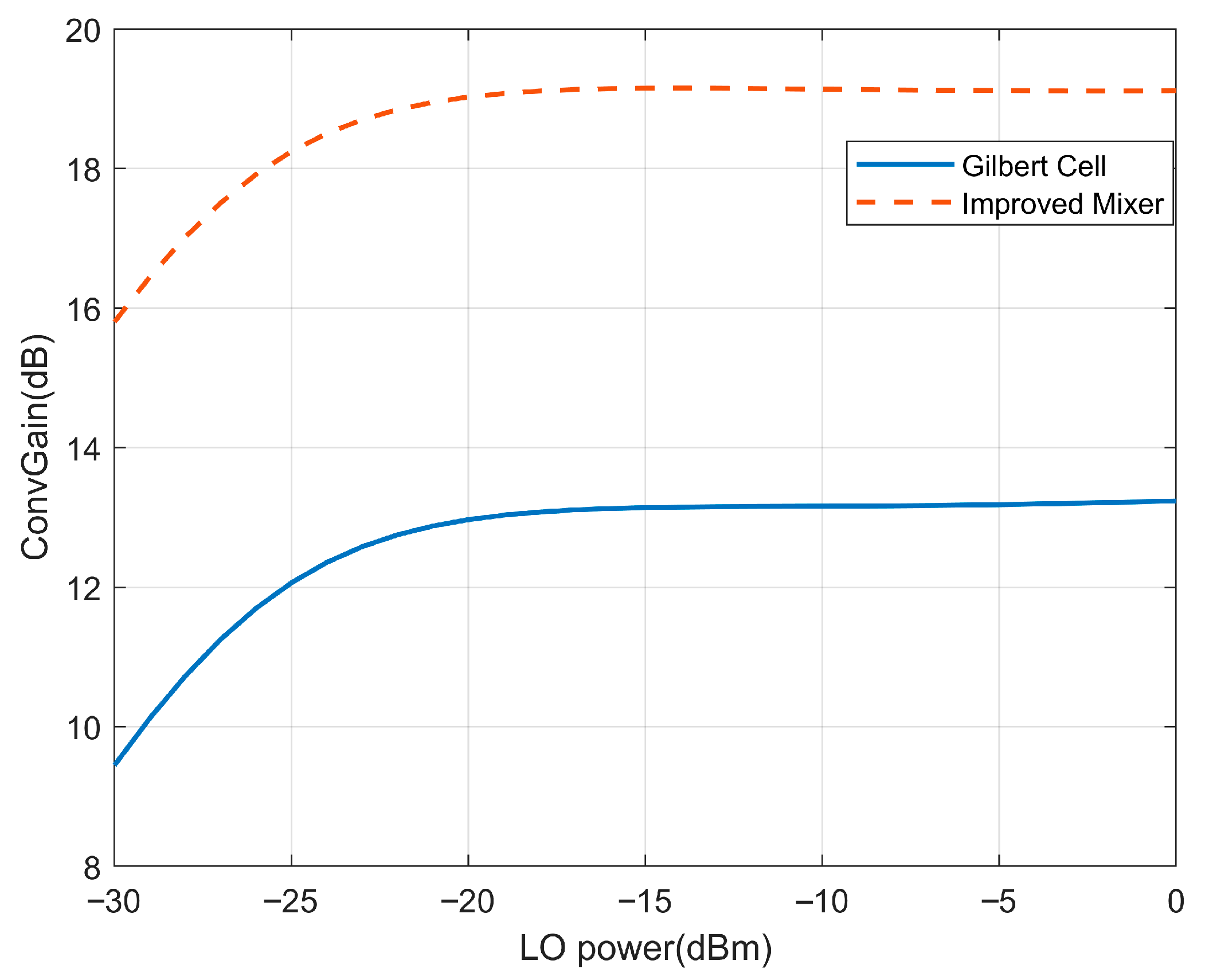
Figure 5 illustrates the conversion gain images of the basic Gilbert-cell-based mixer and the enhanced mixer under identical input conditions. The results show a significant increase in conversion gain for the enhanced mixer, particularly at lower local oscillator power levels, and enhanced stability in conversion gain.
The two graphs illustrate significant enhancements in mixer performance. The original design shows a relationship between conversion gain and LO power, ranging from 8.75 dB at −30 dBm to 12.5 dB at 0 dBm, with conversion loss at lower power levels. The improved mixer demonstrates consistently higher performance, maintaining 15.5–19.5 dB gain across the entire range and reaching saturation at just −20 dBm.
Key improvements include the elimination of conversion loss at low power, an increase in maximum gain from 12.5 dB to 19.5 dB, and a significant reduction in power consumption requirements. The flat response in the saturation region indicates excellent stability against power fluctuations, which simplifies system design and enhances reliability in practical applications where LO power may vary, such as sensor backends.
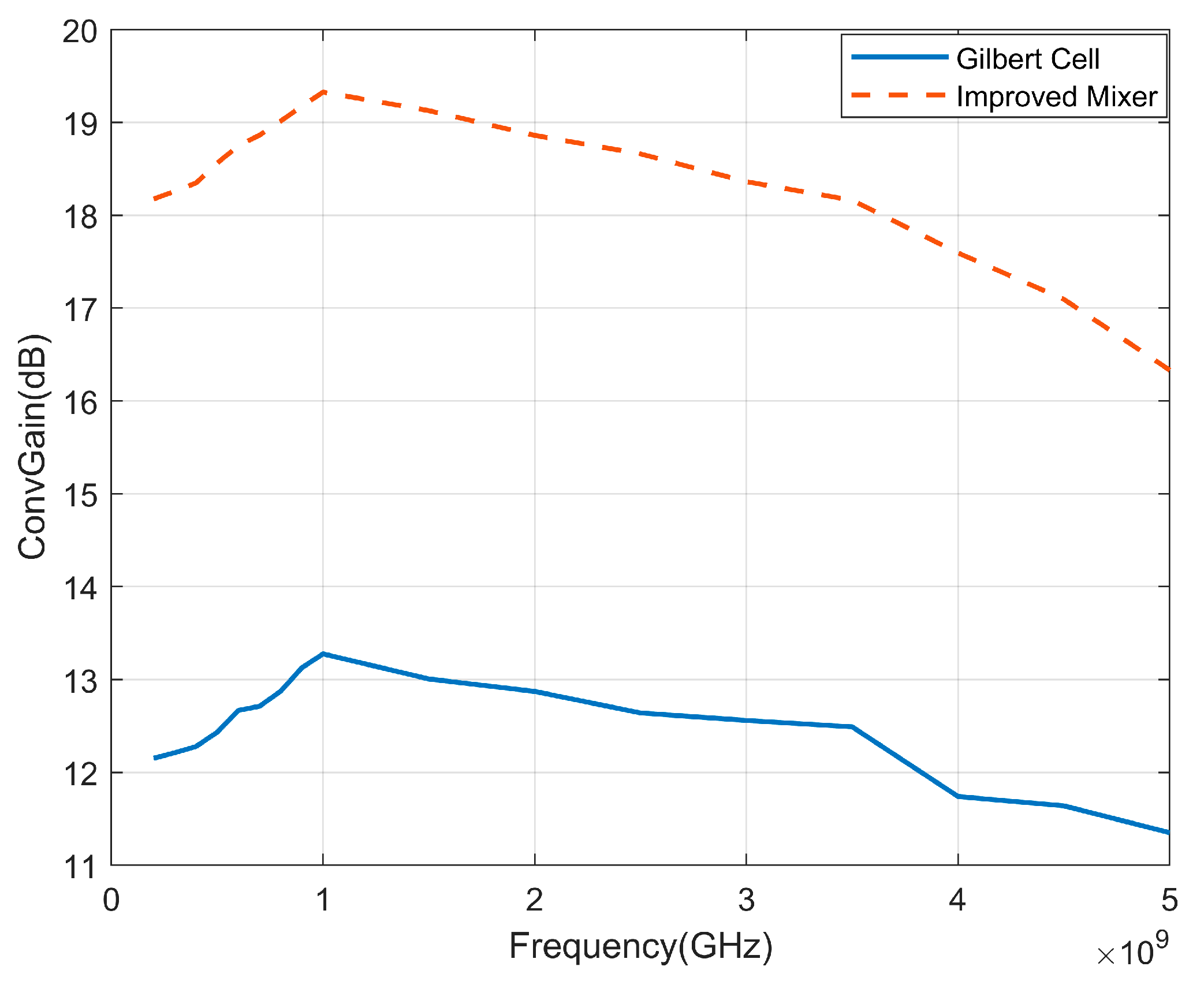
In RF application scenarios, mixers are frequently required to operate across broader frequency ranges, extending well beyond the vicinity of 1 GHz. Under such circumstances, conventional CMOS mixers often experience substantial gain degradation when subjected to variations in RF signal frequency. The improved mixer design, however, demonstrates gain performance characteristics during frequency sweep operations as illustrated in
Figure 6. The flatness of the Gilbert cell and the improved mixer is shown in the figure. The gain stability of the improved mixer is higher than that of the ordinary Gilbert cell. This simulation was conducted under the condition of local oscillator (LO) power at −15 dBm. With power and frequency conditions maintained constant, the results primarily demonstrate the frequency-dependent conversion gain characteristics of the improved mixer. In comparison with
Figure 5, the gain reaches its maximum value of approximately 19.35 dB near 1 GHz. Notably, this enhanced architecture exhibits a stable, gradual decline in gain at elevated frequencies while maintaining positive gain values, thereby providing adequate margin for subsequent stages in the signal chain. This controlled gain reduction characteristic represents a significant advancement over traditional implementations, where performance metrics typically deteriorate rapidly outside narrow operating bands. The enhanced frequency response enables the mixer to function effectively across multiple communication bands without necessitating band-specific circuit optimizations, thus supporting system-level flexibility and multi-standard compatibility requirements increasingly demanded in contemporary wireless applications.
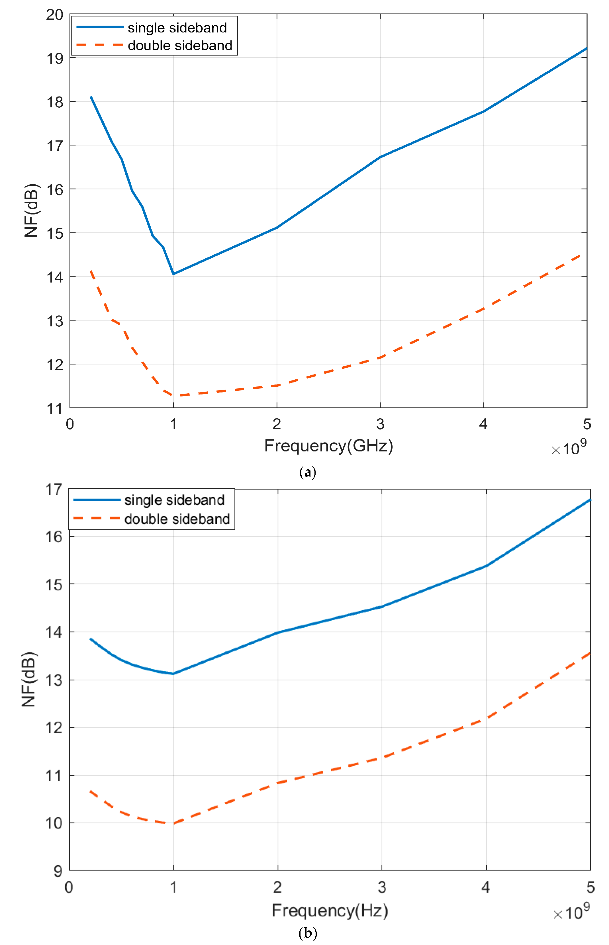
The double-sideband (DSB) mixer implements direct modulation in its simplest form, wherein the baseband signal and carrier signal are combined through a multiplier circuit. The resulting output, after bandpass filtering, contains both upper and lower sidebands symmetrically positioned around the carrier frequency. In contrast, the single-sideband (SSB) mixer employs a quadrature architecture with two orthogonal signal paths. This configuration necessitates 90-degree phase shift networks for both the baseband and carrier signals. Through appropriate addition or subtraction of the quadrature components, either the upper sideband (USB) or lower sideband (LSB) is selectively generated, while the unwanted sideband is inherently suppressed.
Figure 7 illustrates the relationship between single-sideband (SSB) and double-sideband (DSB) noise figures as functions of RF input frequency. The intermediate frequency is fixed at 50 MHz, while the RF input frequency spans from 0 to 5 GHz, with noise figure values ranging approximately from 8 to 17 dB. This simulation was also conducted with the local oscillator (LO) power maintained at −15 dBm. At the frequency of 1 GHz, a comparison can be made with the corresponding LO power level shown in
Figure 5. The results indicate that the noise figures for both single-sideband (SSB) and double-sideband (DSB) configurations demonstrate improvements of approximately 1.5 dB and 4.5 dB, respectively, compared to the original mixer design.
The SSB noise figure consistently remains 3–4 dB below the DSB noise figure throughout the measured spectrum. Both curves exhibit slight U-shaped characteristics across the frequency range, reaching minimum values at approximately 1 GHz before gradually increasing with frequency. The minimum SSB noise figure is approximately 10 dB, while the minimum DSB noise figure is approximately 13.5 dB. These noise characteristics are critical for receiver design considerations, as they directly influence system sensitivity and signal-to-noise ratio performance.
For mixers, the IF port spectrum encompasses various frequency components observable at this port, characterizing intermediate frequency signals, LO feedthrough, mixing products, and harmonics. This directly reflects the mixer’s capability to process higher-order harmonics and identify various spurious components, while revealing non-ideal effects such as LO leakage and RF breakthrough. These phenomena significantly impact the quality and complexity of sensor signal processing, representing the overall design of sensor backend circuitry.
To obtain representative simulation results, the RF is set to 900 MHz, the LO frequency to 850 MHz, the IF to 50 MHz.
Figure 8 depicts the IF spectrum of this mixer, visually demonstrating the downconversion of RF signals to intermediate frequencies. As shown in the figure, the noise floor is approximately –160 dBm, and the power levels vary between −120 dBm and −20 dBm, with specific power levels calculated by converting IF port voltages using ADS harmonic balance analysis. The spectrum displays multiple peaks representing the frequency distribution and relative intensities of IF signals, LO feedthrough, and harmonics after conversion at the IF port, while low-amplitude components represent noise floor and harmonic interference.
The primary IF signal appears prominently in the spectrum, indicating successful frequency translation from the RF input. Secondary peaks corresponding to various mixing products (mfRF ± nfLO) are visible at different frequency offsets, with diminishing amplitudes for higher-order products. The presence and magnitude of these spurious responses provide critical insights into the mixer’s linearity performance and dynamic range limitations. LO feedthrough, appearing at the LO frequency, serves as a key indicator of port-to-port isolation efficiency within the mixer structure.
The strongest component in the IF-port spectrum is the desired 50 MHz IF signal, at approximately –30 dBm. The signals at 100 MHz and 150 MHz correspond to the second and third harmonics, respectively. Components near 200 MHz are predominantly mixing products, whereas those around 750 MHz arise from fractional-harmonic mixing products and spurious signals. The image frequency appears at 800 MHz, LO feedthrough at 850 MHz, and RF leakage at 900 MHz. At higher frequencies, additional second- and third-order mixing products are observed.
The spectral distribution also reflects the mixer’s intermodulation performance, with third-order intermodulation products being particularly significant for system design considerations. The frequency separation between wanted and unwanted components determines the filtering requirements for subsequent stages. Notably, most non-ideal components are sufficiently distant from the target frequency, allowing for removal through subsequent filtering networks without excessive design complexity or insertion loss penalties. This spectral behavior ultimately influences the overall system noise figure, dynamic range, and signal fidelity in the complete sensor signal chain.
For mixers, the frequency composition of noise is highly complex. The impact on mixer performance varies significantly among different noise sources: in-band noise at the input, out-of-band noise in the RF spectrum that may fold into the IF band through mixing, and noise at image frequencies that directly converts to the IF output. Under the influence of noise at different frequencies, the mixer exhibits significant variations in both noise performance and signal processing capability.
In the low-frequency region near DC, 1/f noise dominates. In the mid-frequency region, thermal noise prevails, where device transconductance and parasitic effects remain relatively stable, resulting in a relatively flat noise figure. In the high-frequency region, the influence of phase noise begins to intensify.
Noise folding causes noise from multiple RF frequencies to be down-converted to the same IF. Intermodulation noise arises from nonlinear intermodulation products, while local oscillator noise produces reciprocal mixing. The harmonic noise at the LO port induces additional frequency conversion, while LO leakage feeds through directly to the output and causes DC offset in direct conversion architectures. Consequently, mixer design considerations encompass avoiding image frequency interference, mitigating harmonic mixing effects, and optimizing IF selection, among other aspects.
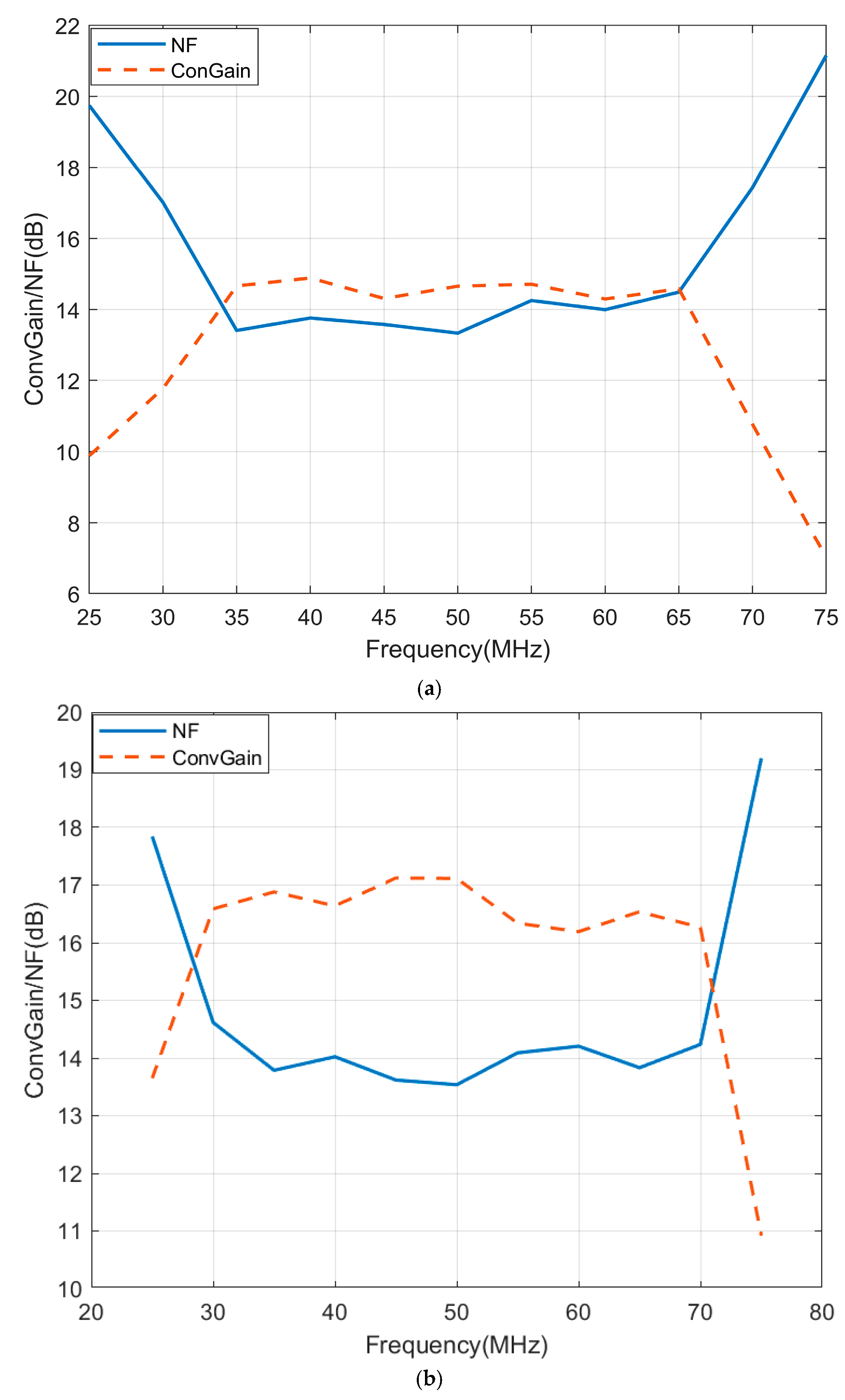
Figure 9 illustrates the variations in noise figure and conversion gain with noise frequency for both the conventional Gilbert cell and the improved mixer. Both parameters are significantly enhanced in the improved design. Notably, the noise suppression range of the Gilbert cell is approximately 35–65 MHz, whereas the improved mixer effectively suppresses noise over a wider range of 30–70 MHz. Within this range, the noise figure remains relatively low and stable without pronounced fluctuations, indicating that the proposed design extends the bandwidth over which noise can be effectively managed. The conversion gain also reaches relatively higher levels within this frequency band without excessive discontinuities.
Consequently, the optimal application range for this mixer is primarily within the 30–70 MHz noise frequency band, which determines the extent of noise influence on the sensor backend. As depicted in
Figure 9, when noise frequencies fall below 30 MHz or exceed 70 MHz, the noise figure rapidly increases while the conversion gain sharply decreases. This behavior reflects the mixer’s susceptibility to degraded performance at excessively low or high frequencies, emphasizing its specialization in processing noise within the 30–70 MHz range.
This frequency-dependent performance characteristic provides valuable guidance for system integration, indicating that subsequent filtering and amplification stages should be optimized for operation within this specific frequency band to maintain optimal signal-to-noise ratio throughout the signal processing chain.
In the RF receiver at the sensor backend, employing a dual-conversion architecture that achieves the final target frequency through two frequency conversions can more effectively separate and suppress image frequency interference. After the first frequency conversion, the frequency separation between the image frequency and the useful signal becomes larger, facilitating filter design. In the dual-conversion structure, the substantial frequency difference between the first local oscillator and the RF signal reduces local oscillator leakage to the antenna, thereby improving the electromagnetic compatibility of the receiver. Additionally, gain control can be implemented at both intermediate frequency stages, enabling adaptation to input signals of varying strengths. Through judicious selection of the two local oscillator frequencies, the phase noise performance of the entire system can be optimized when processing weak signals.
The dual-conversion architecture is illustrated in
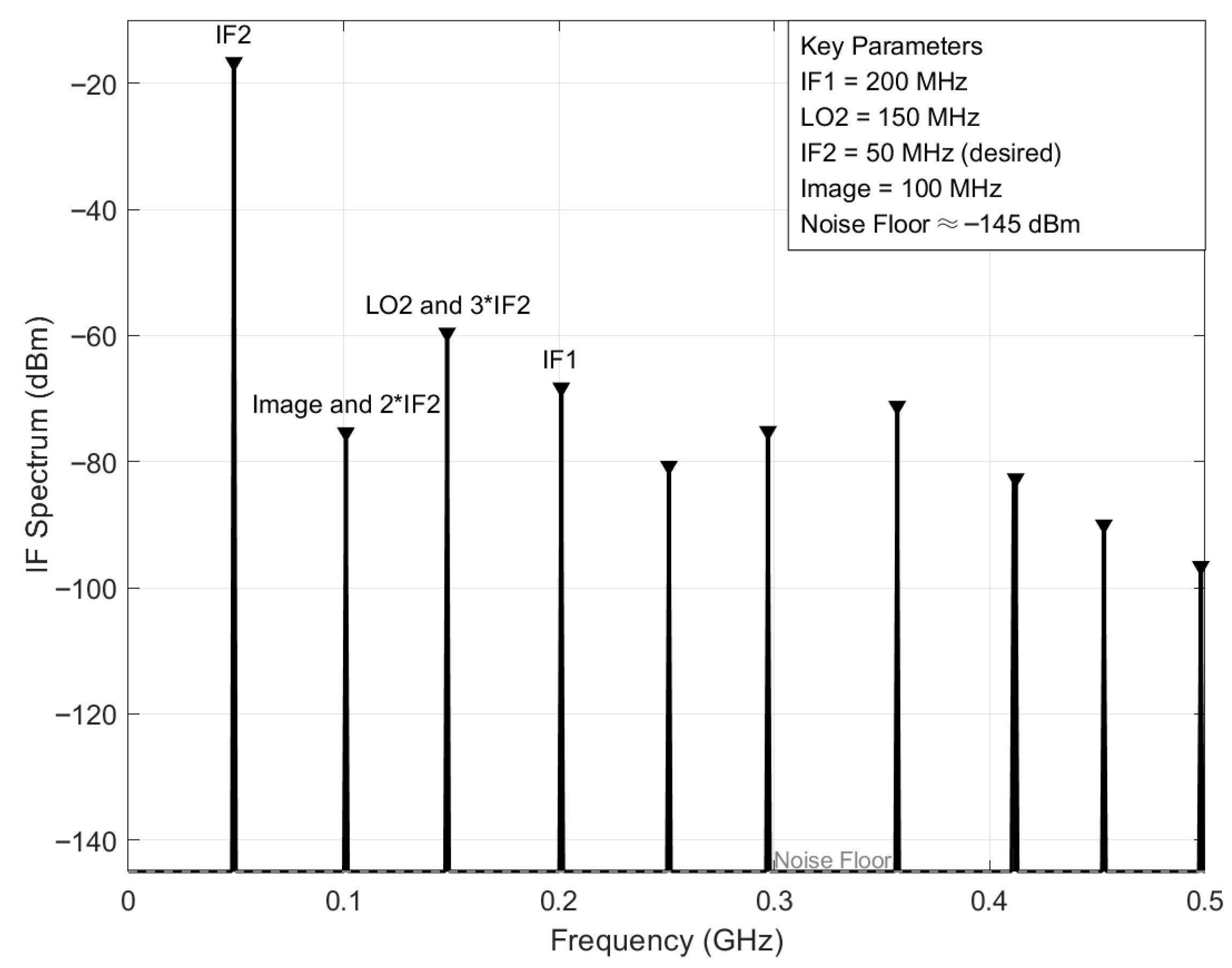
Figure 10, where both mixing stages can employ fundamental mixers. The improved mixer design can accommodate a wide input frequency range and remains applicable even at higher frequency bands exceeding 1 GHz. The RF input is set to 2 GHz with accompanying image frequency inputs. The center frequency of bandpass filter BFP2 is also configured at 2 GHz (matching the RF input) with a bandwidth of 10 MHz and 1 dB ripple. After filtering, the RF input undergoes downconversion in the mixer with the first local oscillator input at 1800 MHz, yielding a first intermediate frequency of 200 MHz. Bandpass filter BFP1 has a center frequency of 200 MHz, a bandwidth of 1 MHz, and 1 dB ripple. The first intermediate frequency is subsequently mixed with the second local oscillator input at 150 MHz after filtering, producing the final intermediate frequency of 50 MHz.
Compared to the single-stage mixing discussed above, the dual-conversion architecture achieves superior image frequency suppression, with signal strength at the image frequency significantly reduced. Additionally, the substantial frequency separation between the first local oscillator and the RF signal improves local oscillator leakage performance. Consequently, this configuration enhances the RF input frequency range that the mixer can accommodate, demonstrating satisfactory performance even at 2 GHz input frequencies.
Figure 11 illustrates the signal response under a dual-conversion architecture configuration. As demonstrated in the figure, the low-frequency region exhibits densely packed spectral components with peak amplitudes approaching 0 dBm. The overall spectrum reveals various frequency combinations and harmonics generated by two-stage mixing, with the low-frequency domain encompassing multiple intermediate frequency signals, image frequency signals, and certain intermodulation products.
This spectral distribution primarily reflects the dual-conversion architecture’s processing of different frequency components based on this mixer design, particularly its effective suppression of image frequencies. The architecture employs two-stage frequency conversion, thereby enhancing overall power performance. The second-stage frequency conversion merely involves the conversion from 200 MHz to 50 MHz, which substantially reduces the implementation complexity. In the vicinity of the target frequency, only the second-stage image frequencies, leakage, and harmonics are present, significantly reducing interference from non-ideal frequency components on the mixing results. This provides greater design margin for subsequent sensor backend signal processing stages. This architecture is capable of handling higher-frequency RF inputs while maintaining superior image rejection and harmonic suppression performance, demonstrating the improved mixer’s applicability across broader frequency scenarios and its complete suitability for higher frequency applications.
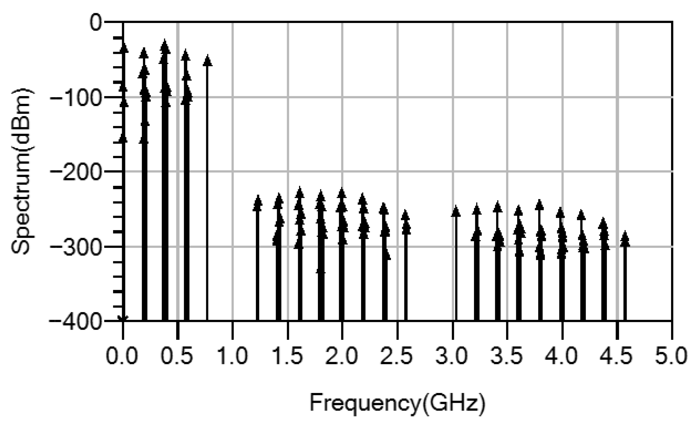
Figure 12 presents a harmonic balance analysis of the dual-conversion system, with frequency ranging from 0 to 5 GHz on the horizontal axis and power spectral density from −400 to 0 dBm on the vertical axis. The spectrum reveals dense frequency components in the low-frequency region with the strongest signal content. Between 1.2 and 2.6 GHz, spectral intensity decreases significantly, predominantly exhibiting spurious emissions and harmonics. At the 3–4.6 GHz high-frequency range, another distinct signal group appears.
This spectrum demonstrates various products from two-stage mixing, including IF output, image signals, LO leakage, intermodulation components, and RF feedthrough.
Figure 12 employs iterative steady-state frequency domain analysis, revealing additional discrete spectral components that better characterize harmonics and intermodulation products. This method proves more efficient for large-signal steady-state analysis, providing enhanced visibility of frequency domain interactions within the dual-conversion architecture.
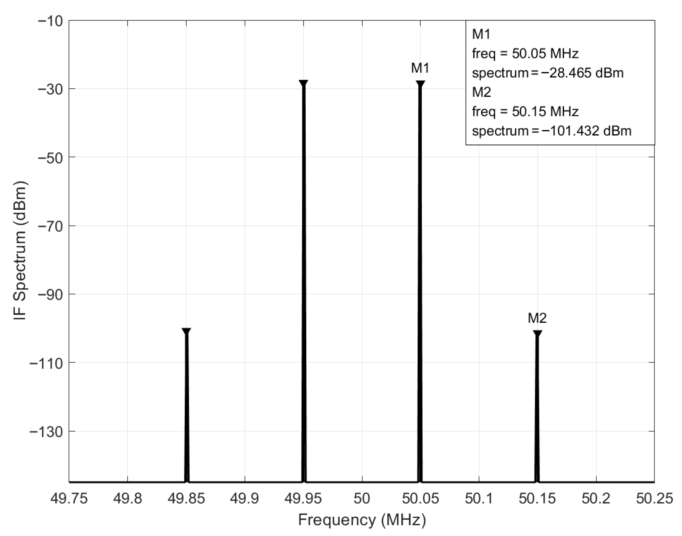
Figure 13 presents an output spectrum analysis utilizing harmonic balance to evaluate image rejection performance and third-order intercept (TOI) point near the intermediate frequency. Harmonic balance demonstrates superior accuracy in analyzing nonlinear effects including mixing and harmonic distortion, where conventional methods may fail to capture nonlinear behavior adequately.
The frequency range and power spectral density are represented on the horizontal and vertical axes, respectively, displaying signal distribution around the 50 MHz IF. This simulation employs conditions similar to those described previously and is likewise based on the circuit topology shown in
Figure 10. However, the purpose of this simulation is to test the third-order intercept point rather than the image frequency rejection examined earlier, necessitating different input conditions. The RF input consists of two test signals with a tone spacing of 100 kHz, which, after dual conversion, yield signals at 49.95 MHz and 50.05 MHz at the second intermediate frequency. This simulation focuses on a narrow frequency band around the target frequency. As illustrated in
Figure 13, the components at 49.85 MHz and 50.15 MHz are third-order intermodulation products. The TOI is calculated as the difference between 1.5 times the fundamental power and 0.5 times the third-order intermodulation power, yielding 8.0185 dBm.
These simulation results clearly demonstrate the mixer’s output characteristics near the IF band. The design successfully integrates multiple performance aspects including noise management, conversion gain optimization, and effective suppression of non-ideal components, validating its comprehensive performance.
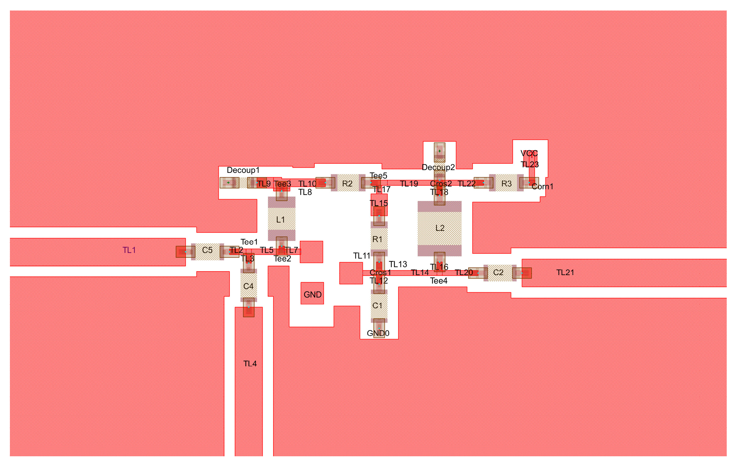
In mixer design, the physical layout realization plays a crucial role due to transmission line losses, structural discontinuities, and impedance mismatch effects. The layout of the proposed design is illustrated in
Figure 14, where microstrip lines are employed for interconnection. Impedance control is achieved through rectangular traces with fixed widths, while phase adjustment and impedance transformation are realized by varying the transmission line lengths. The RF signal path is minimized to the greatest extent possible, with decoupling implemented at multiple locations to reduce losses through compact layout. The transmission line TL1 on the left side serves as the RF input, the transmission line TL4 at the bottom serves as the LO input, and the transmission line TL21 on the right side serves as the IF output.
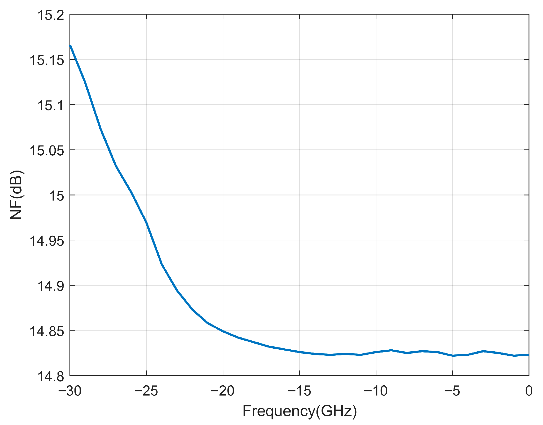
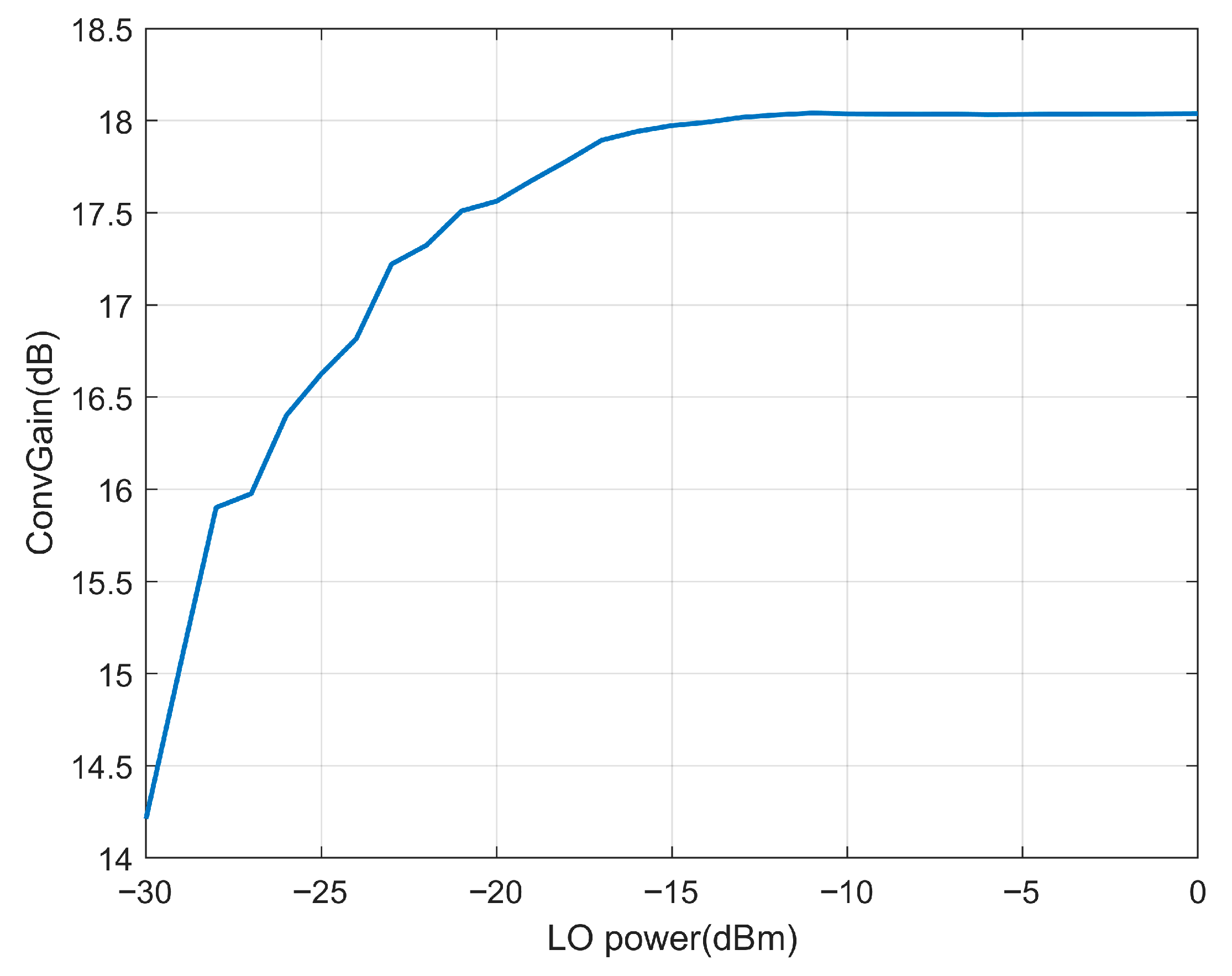
To evaluate the post-layout performance, Momentum electromagnetic simulation was conducted on the layout to extract multi-port S-parameters. These extracted parameters were then incorporated into the schematic simulation to replace ideal transmission line models, thereby accounting for parasitic effects, grounding impacts, and other layout-induced parasitics. This approach enables a comprehensive assessment of the mixer performance including electromagnetic effects. The final noise figure simulation results incorporating layout effects are presented in
Figure 15, while the corresponding conversion gain results are illustrated in
Figure 16.
Figure 15 demonstrates that, under equivalent simulation conditions, the layout-based noise figure exceeds the pre-layout ideal results from
Figure 4 by approximately 0.5–1.5 dB. This performance degradation is primarily caused by transmission line losses that directly elevate the system noise figure. The proposed design exhibits relatively consistent noise increase characteristics.
Figure 16 reveals that the layout-derived conversion gain is reduced by approximately 1–2 dB compared to the ideal case shown in
Figure 5. This performance reduction can be attributed to microstrip line losses, discontinuities arising from interconnection pads, and impedance mismatches present in the physical layout implementation. Notably, the conversion gain dependence on LO power maintains good stability in the layout simulation, indicating suitability for practical sensor interface applications.
5. Conclusions
This design employs a process incorporating high-quality BJTs and adopts a mixer-first architecture. By leveraging the noise and linearity advantages of BJTs, it overcomes the performance limitations of CMOS mixers while reducing reliance on the LNA at the system-architecture level, thereby simplifying the front-end and enhancing robustness. The flexibility of BJTs is exploited at both the front-end and intermediate-frequency output stages to optimize input impedance and matching. Differential structures are laid out with strict symmetry, achieving DC and RF isolation.
In summary, mixers employing BJTs and enhanced impedance matching can significantly enhance the noise figure and conversion gain. While this may result in increased power consumption, these mixers can be further optimized for use in high-performance RF frontends, meeting overall performance demands.
Table 1 summarizes the performance comparison of conversion gain and noise between the Gilbert cell and the improved mixer. It can be observed that the improved mixer exhibits significantly lower noise and higher conversion gain.
Furthermore, in the multi-frequency conversion response analysis conducted at the intermediate frequency port, the improved mixer demonstrates significantly lower conversion loss, a flatter frequency response, and excellent third-order intercept point performance, indicating superior linearity and the capability to handle larger input signals without severe distortion. The enhanced mixer exhibits superior LO-IF isolation, which effectively suppresses local oscillator feedthrough. Through direct measurement and response analysis, it can be observed that the image rejection ratio and dual-peak response have been well addressed, with reduced conversion efficiency for image frequencies, all of which demonstrate significant improvement in image frequency suppression for the improved filter.
The enhanced performance characteristics of this improved mixer hold significant implications for sensor backend applications, where signal integrity and processing accuracy are paramount. In modern sensor systems, particularly those operating in challenging electromagnetic environments, the superior linearity and reduced harmonic distortion directly translate to improved signal-to-noise ratio and enhanced measurement precision. The flatter frequency response ensures consistent performance across the operational bandwidth, which is crucial for wideband sensor applications such as radar systems, spectrum analyzers, and communication receivers where frequency-dependent gain variations can introduce measurement errors.
The improved image rejection capability is particularly valuable in heterodyne receiver architectures commonly employed in sensor backends, where unwanted image frequency responses can lead to false target detection or signal misinterpretation. The enhanced LO-IF isolation minimizes local oscillator leakage, thereby reducing spurious signals that could compromise the dynamic range and sensitivity of the sensor system. Furthermore, the superior third-order intercept point enables the mixer to maintain linear operation even when processing high-amplitude signals, which is essential in applications where the sensor must simultaneously handle both weak and strong signals without intermodulation distortion.
These improvements collectively contribute to enhanced system reliability and measurement accuracy in critical sensor applications, including defense radar systems, medical imaging equipment, and precision instrumentation, where the backend processing chain must maintain signal fidelity throughout the frequency conversion process while operating under stringent performance requirements.
