Direct Writing of Metal Nanostructures with Focused Helium Ion Beams
Abstract
1. Introduction
2. Methods
3. Results
4. Conclusions
Supplementary Materials
Author Contributions
Funding
Data Availability Statement
Acknowledgments
Conflicts of Interest
References
- He, S.; Tian, R.; Wu, W.; Li, W.-D.; Wang, D. Helium-ion-beam nanofabrication: Extreme processes and applications. Int. J. Extrem. Manuf. 2021, 3, 012001. [Google Scholar] [CrossRef]
- Allen, F.I. A review of defect engineering, ion implantation, and nanofabrication using the helium ion microscope. Beilstein J. Nanotechnol. 2021, 12, 633–664. [Google Scholar] [CrossRef] [PubMed]
- Nakaharai, S.; Iijima, T.; Ogawa, S.; Suzuki, S.; Li, S.-L.; Tsukagoshi, K.; Sato, S.; Yokoyama, N. Conduction Tuning of Graphene Based on Defect-Induced Localization. Acs Nano 2013, 7, 5694–5700. [Google Scholar] [CrossRef] [PubMed]
- Huang, Z.; Li, W.-D.; Santori, C.; Acosta, V.M.; Faraon, A.; Ishikawa, T.; Wu, W.; Winston, D.; Williams, R.S.; Beausoleil, R.G. Diamond nitrogen-vacancy centers created by scanning focused helium ion beam and annealing. Appl. Phys. Lett. 2013, 103, 081906. [Google Scholar] [CrossRef]
- Cybart, S.A.; Cho, E.Y.; Wong, T.J.; Wehlin, B.H.; Ma, M.K.; Huynh, C.; Dynes, R.C. Nano Josephson superconducting tunnel junctions in YBa2Cu3O7–δ directly patterned with a focused helium ion beam. Nat. Nanotechnol. 2015, 10, 598–602. [Google Scholar] [CrossRef]
- Kasaei, L.; Manichev, V.; Li, M.; Feldman, L.C.; Gustafsson, T.; Collantes, Y.; Hellstrom, E.; Demir, M.; Acharya, N.; Bhattarai, P.; et al. Normal-state and superconducting properties of Co-doped BaFe2As2 and MgB2 thin films after focused helium ion beam irradiation. Supercond. Sci. Technol. 2019, 32, 095009. [Google Scholar] [CrossRef]
- Kamenov, P. Superconducting Quantum Circuits Based on Disordered Aluminum Films. Ph.D. Thesis, Rutgers, The State University of New Jersey, New Brunswick, NJ, USA, 2023. [Google Scholar] [CrossRef]
- Xiang, B.; Wang, Y.; Li, H.; Cybart, S.A. Fabrication and Application of Nano-SQUID Magnetometer to Scanning Imaging of Two-Dimensional Quantum Materials. EMScience 2024, 2, 0060131. [Google Scholar] [CrossRef]
- Prewett, P.D.; Hagen, C.W.; Lenk, C.; Lenk, S.; Kaestner, M.; Ivanov, T.; Ahmad, A.; Rangelow, I.W.; Shi, X.; Boden, S.A.; et al. Charged particle single nanometre manufacturing. Beilstein J. Nanotechnol. 2018, 9, 2855–2882. [Google Scholar] [CrossRef] [PubMed]
- Toulouse, C.; Fischer, J.; Farokhipoor, S.; Yedra, L.; Carlà, F.; Jarnac, A.; Elkaim, E.; Fertey, P.; Audinot, J.N.; Wirtz, T.; et al. Patterning enhanced tetragonality in BiFeO3 thin films with effective negative pressure by helium implantation. Phys. Rev. Mater. 2021, 5, 024404. [Google Scholar] [CrossRef]
- Fenner, D.; DiFilippo, V.; Bennett, J.; Tetreault, T.; Hirvonen, J.; Feldman, L. Ion beam nanosmoothing of sapphire and silicon carbide surfaces. In Proceedings of the International Symposium on Optical Science and Technology, San Diego, CA, USA, 29 July–3 August 2001; Volume 4468. [Google Scholar]
- Iberi, V.; Vlassiouk, I.; Zhang, X.G.; Matola, B.; Linn, A.; Joy, D.C.; Rondinone, A.J. Maskless Lithography and in situ Visualization of Conductivity of Graphene using Helium Ion Microscopy. Sci. Rep. 2015, 5, 11952. [Google Scholar] [CrossRef]
- Zhang, L.; Heinig, N.F.; Bazargan, S.; Abd-Ellah, M.; Moghimi, N.; Leung, K.T. Direct-write three-dimensional nanofabrication of nanopyramids and nanocones on Si by nanotumefaction using a helium ion microscope. Nanotechnology 2015, 26, 255303. [Google Scholar] [CrossRef] [PubMed]
- van Dorp, W.F.; Hagen, C.W. A critical literature review of focused electron beam induced deposition. J. Appl. Phys. 2008, 104, 081301. [Google Scholar] [CrossRef]
- Boden, S.A.; Moktadir, Z.; Bagnall, D.M.; Mizuta, H.; Rutt, H.N. Focused helium ion beam milling and deposition. Microelectron. Eng. 2011, 88, 2452–2455. [Google Scholar] [CrossRef]
- Höflich, K.; Maćkosz, K.; Jureddy, C.S.; Tsarapkin, A.; Utke, I. Direct electron beam writing of silver using a β-diketonate precursor: First insights. Beilstein J. Nanotechnol. 2024, 15, 1117–1124. [Google Scholar] [CrossRef]
- Kohama, K.; Iijima, T.; Hayashida, M.; Ogawa, S. Tungsten-based pillar deposition by helium ion microscope and beam-induced substrate damage. J. Vac. Sci. Technol. B 2013, 31, 031802. [Google Scholar] [CrossRef]
- Wagner, A.; Levin, J.P.; Mauer, J.L.; Blauner, P.G.; Kirch, S.J.; Longo, P. X-Ray Mask Repair with Focused Ion-Beams. J. Vac. Sci. Technol. B 1990, 8, 1557–1564. [Google Scholar] [CrossRef]
- Sanford, C.A.; Stern, L.; Barriss, L.; Farkas, L.; DiManna, M.; Mello, R.; Maas, D.J.; Alkemade, P.F.A. Beam induced deposition of platinum using a helium ion microscope. J. Vac. Sci. Technol. B Microelectron. Nanometer Struct. Process. Meas. Phenom. 2009, 27, 2660–2667. [Google Scholar] [CrossRef]
- Chen, P.; Veldhoven, E.v.; Sanford, C.A.; Salemink, H.W.M.; Maas, D.J.; Smith, D.A.; Rack, P.D.; Alkemade, P.F.A. Nanopillar growth by focused helium ion-beam-induced deposition. Nanotechnology 2010, 21, 455302. [Google Scholar]
- Scipioni, L.; Sanford, C.; van Veldhoven, E.; Maas, D. A Design-of-Experiments Approach to Characterizing Beam-Induced Deposition in the Helium Ion Microscope. Microsc. Today 2011, 19, 22–26. [Google Scholar] [CrossRef]
- Wu, H.M.; Stern, L.A.; Chen, J.H.; Huth, M.; Schwalb, C.H.; Winhold, M.; Porrati, F.; Gonzalez, C.M.; Timilsina, R.; Rack, P.D. Synthesis of nanowires via helium and neon focused ion beam induced deposition with the gas field ion microscope. Nanotechnology 2013, 24, 175302. [Google Scholar] [CrossRef]
- Hill, R.M. Electrical Conduction in Ultra Thin Metal Films II. Experimental. Proc. R. Soc. Lond. A Math. Phys. Sci. 1969, 309, 397–417. [Google Scholar]
- Hill, R.M.; Mott, N.F. Electrical conduction in ultra thin metal films I. Theoretical. Proc. R. Soc. Lond. A Math. Phys. Sci. 1969, 309, 377–395. [Google Scholar]
- Parylene Properties. Available online: https://scscoatings.com/parylene-coatings/parylene-properties/ (accessed on 11 November 2024).
- Podzorov, V.; Pudalov, V.M.; Gershenson, M.E. Field-effect transistors on rubrene single crystals with parylene gate insulator. Appl. Phys. Lett. 2003, 82, 1739–1741. [Google Scholar] [CrossRef]
- Podzorov, V.; Gershenson, M.E.; Kloc, C.; Zeis, R.; Bucher, E. High-mobility field-effect transistors based on transition metal dichalcogenides. Appl. Phys. Lett. 2004, 84, 3301–3303. [Google Scholar] [CrossRef]
- Gluschke, J.G.; Richter, F.; Micolich, A.P. A parylene coating system specifically designed for producing ultra-thin films for nanoscale device applications. Rev. Sci. Instrum. 2019, 90, 083901. [Google Scholar] [CrossRef]
- Bruevich, V.; Kasaei, L.; Rangan, S.; Hijazi, H.; Zhang, Z.; Emge, T.; Andrei, E.Y.; Bartynski, R.A.; Feldman, L.C.; Podzorov, V. Intrinsic (Trap-Free) Transistors Based on Epitaxial Single-Crystal Perovskites. Adv. Mater. 2022, 34, 2205055. [Google Scholar] [CrossRef]
- Podzorov, V. Technical Notes. Available online: http://www.physics.rutgers.edu/~podzorov/technicalnotes.php (accessed on 11 November 2024).
- Ziegler, J.F.; Ziegler, M.D.; Biersack, J.P. SRIM—The stopping and range of ions in matter. Nucl. Instrum. Methods Phys. Res. Sect. B Beam Interact. Mater. At. 2010, 268, 1818–1823. [Google Scholar] [CrossRef]
- White, C.W.; Farlow, G.; Narayan, J.; Clark, G.J.; Baglin, J.E.E. Ion beam mixing of metal films on SiO2. Mater. Lett. 1984, 2, 367–372. [Google Scholar] [CrossRef]
- Studzinskii, V.; Fedorenko, E.; Klevtsov, A.; Karaseov, P. Tunable formation of gold nanoparticles on polymer by keV ion beam irradiation. Radiat. Eff. Defect. Solids 2024, 179, 25–32. [Google Scholar] [CrossRef]
- Kosińska, A.; Jagielski, J.; Bieliński, D.M.; Urbanek, O.; Wilczopolska, M.; Frelek-Kozak, M.; Zaborowska, A.; Wyszkowska, E.; Jóźwik, I. Structural and chemical changes in He+ bombarded polymers and related performance properties. J. Appl. Phys. 2022, 132, 074701. [Google Scholar] [CrossRef]
- Bidlack, F.B.; Huynh, C.; Marshman, J.; Goetze, B. Helium ion microscopy of enamel crystallites and extracellular tooth enamel matrix. Front. Physiol. 2014, 5, 395. [Google Scholar] [CrossRef] [PubMed]
- Northby, J.A.; Jiang, T.; Takaoka, G.H.; Yamada, I.; Brown, W.L.; Sosnowski, M. A method and apparatus for surface modification by gas-cluster ion impact. Nucl. Instrum. Methods Phys. Res. Sect. B Beam Interact. Mater. At. 1993, 74, 336–340. [Google Scholar] [CrossRef]
- Voorhees, P.W. The theory of Ostwald ripening. J. Stat. Phys. 1985, 38, 231–252. [Google Scholar] [CrossRef]


| (Ω/sq.) | (Ω·cm)  | d (nm)  | Dose (cm−2) | |
|---|---|---|---|---|
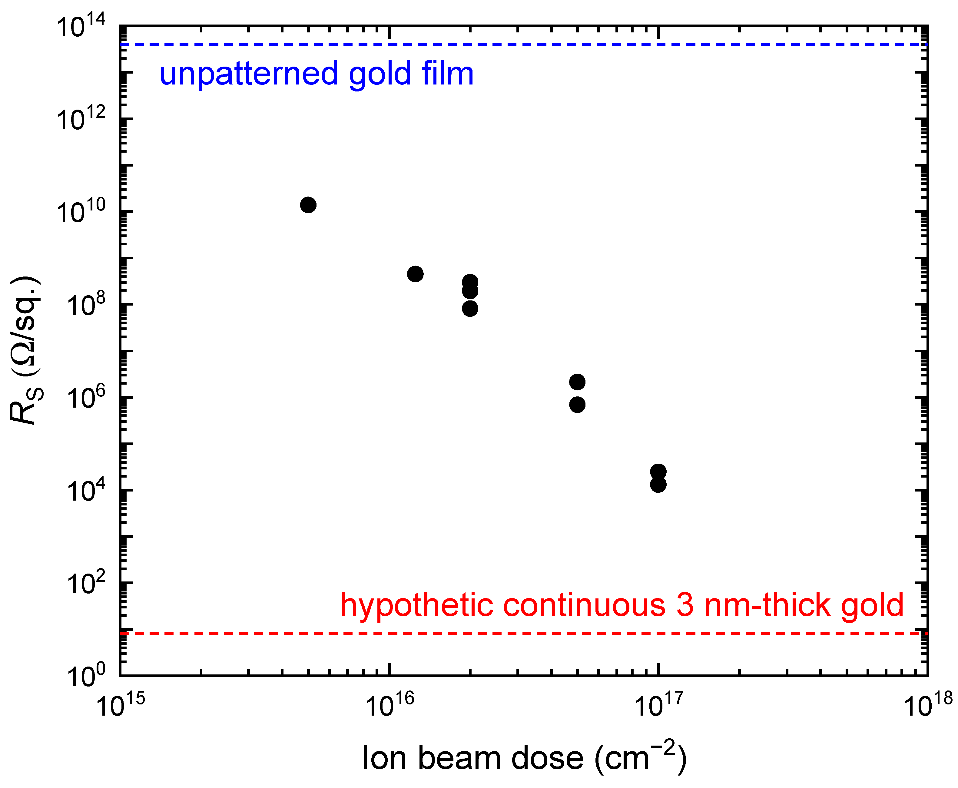
| As-evaporated (unpatterned) ultrathin seed gold film on parylene-N | 4 × 10¹³ | 1.3 × 10⁷ | 3.3 | 0 |
| The same film after the HIM patterning | 7 × 10⁶ | 2.3 | 3.3 | 2 × 10¹⁶ |
| As-grown (unpatterned) parylene-N alone (no gold) | >4 × 10¹⁵ | 1000 | 0 | |
| The same (gold-free) parylene-N after the HIM patterning | 2 × 10¹³ | 1000 | 2 × 10¹⁶ |
 for the gold film, a nominal thickness, , as measured using a quartz crystal microbalance thickness monitor during the thermal evaporation, is indicated. For parylene-N, was determined by optical ellipsometry. The accuracy of the thickness measurements is about 10%.
  the nominal bulk resistivity of the gold film calculated as . For bare parylene-N, the sheet resistance of both unpatterned and patterned films is likely dominated by very small near-surface/surface conductivity, making the estimates of bulk resistivity, in this case, inaccurate.
Disclaimer/Publisher’s Note: The statements, opinions and data contained in all publications are solely those of the individual author(s) and contributor(s) and not of MDPI and/or the editor(s). MDPI and/or the editor(s) disclaim responsibility for any injury to people or property resulting from any ideas, methods, instructions or products referred to in the content. |
© 2024 by the authors. Licensee MDPI, Basel, Switzerland. This article is an open access article distributed under the terms and conditions of the Creative Commons Attribution (CC BY) license (https://creativecommons.org/licenses/by/4.0/).
Share and Cite
Bruevich, V.; Kasaei, L.; Feldman, L.C.; Podzorov, V. Direct Writing of Metal Nanostructures with Focused Helium Ion Beams. Electron. Mater. 2024, 5, 293-302. https://doi.org/10.3390/electronicmat5040018
Bruevich V, Kasaei L, Feldman LC, Podzorov V. Direct Writing of Metal Nanostructures with Focused Helium Ion Beams. Electronic Materials. 2024; 5(4):293-302. https://doi.org/10.3390/electronicmat5040018
Chicago/Turabian StyleBruevich, Vladimir, Leila Kasaei, Leonard C. Feldman, and Vitaly Podzorov. 2024. "Direct Writing of Metal Nanostructures with Focused Helium Ion Beams" Electronic Materials 5, no. 4: 293-302. https://doi.org/10.3390/electronicmat5040018
APA StyleBruevich, V., Kasaei, L., Feldman, L. C., & Podzorov, V. (2024). Direct Writing of Metal Nanostructures with Focused Helium Ion Beams. Electronic Materials, 5(4), 293-302. https://doi.org/10.3390/electronicmat5040018


