
Bayesian Optimization of Hubbard U’s for Investigating InGaN Superlattices

 , , and
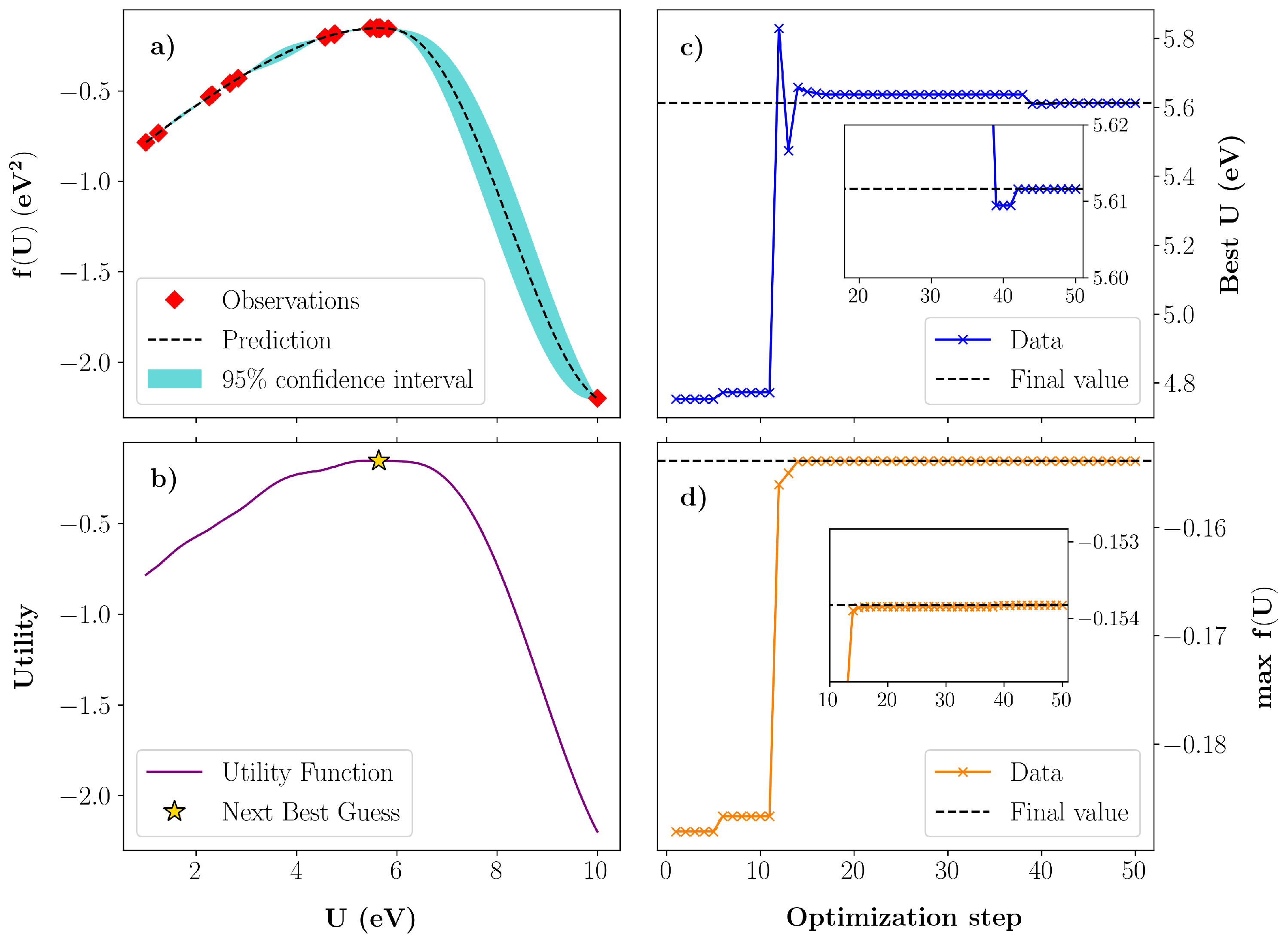
Abstract
:1. Introduction
2. Materials and Methods
2.1. Density Functional Calculations
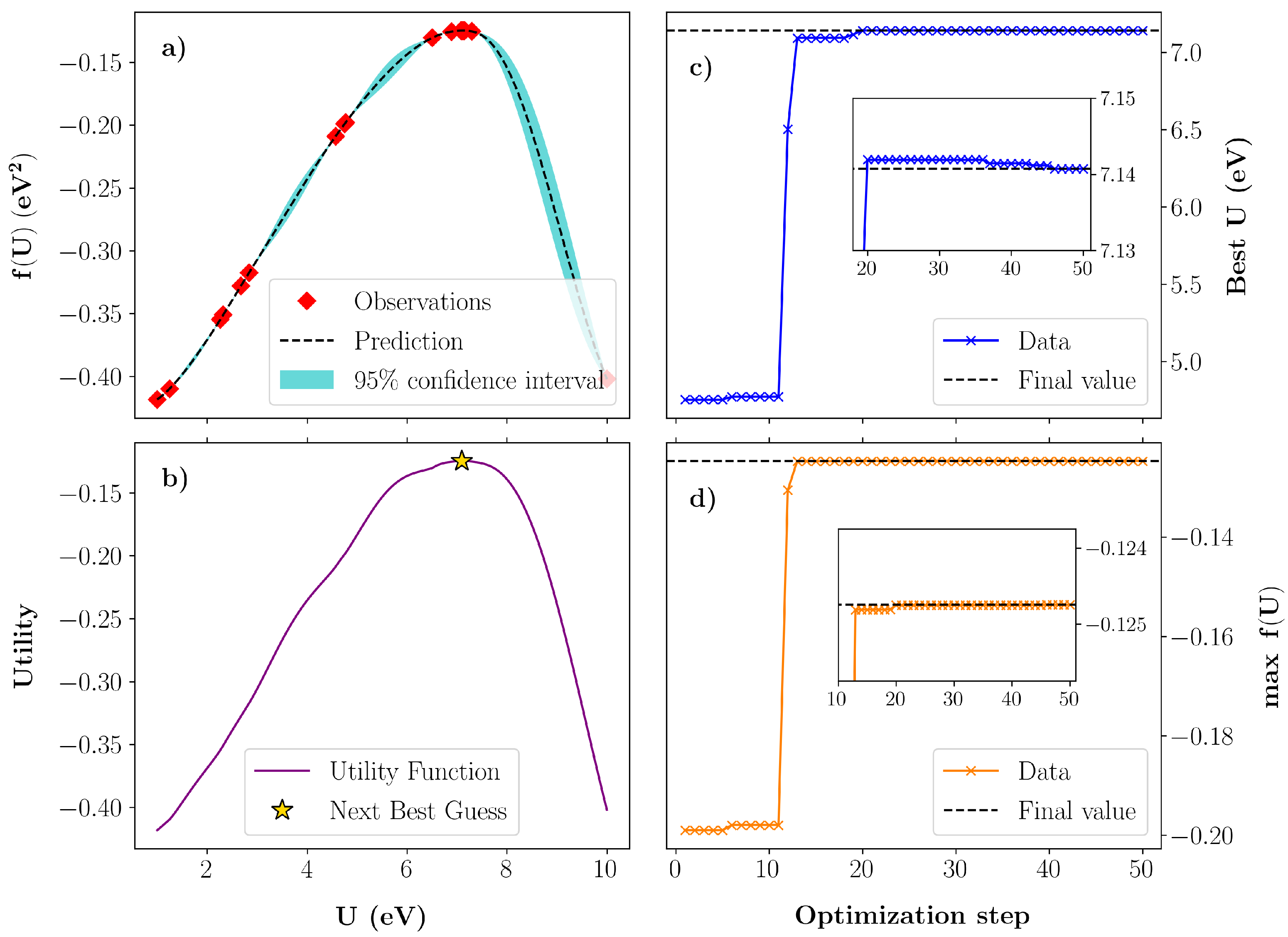
2.2. Bayesian Optimization
3. Results
3.1. Bayesian Optimization of U in GaN
3.2. Bayesian Optimization of U in InN
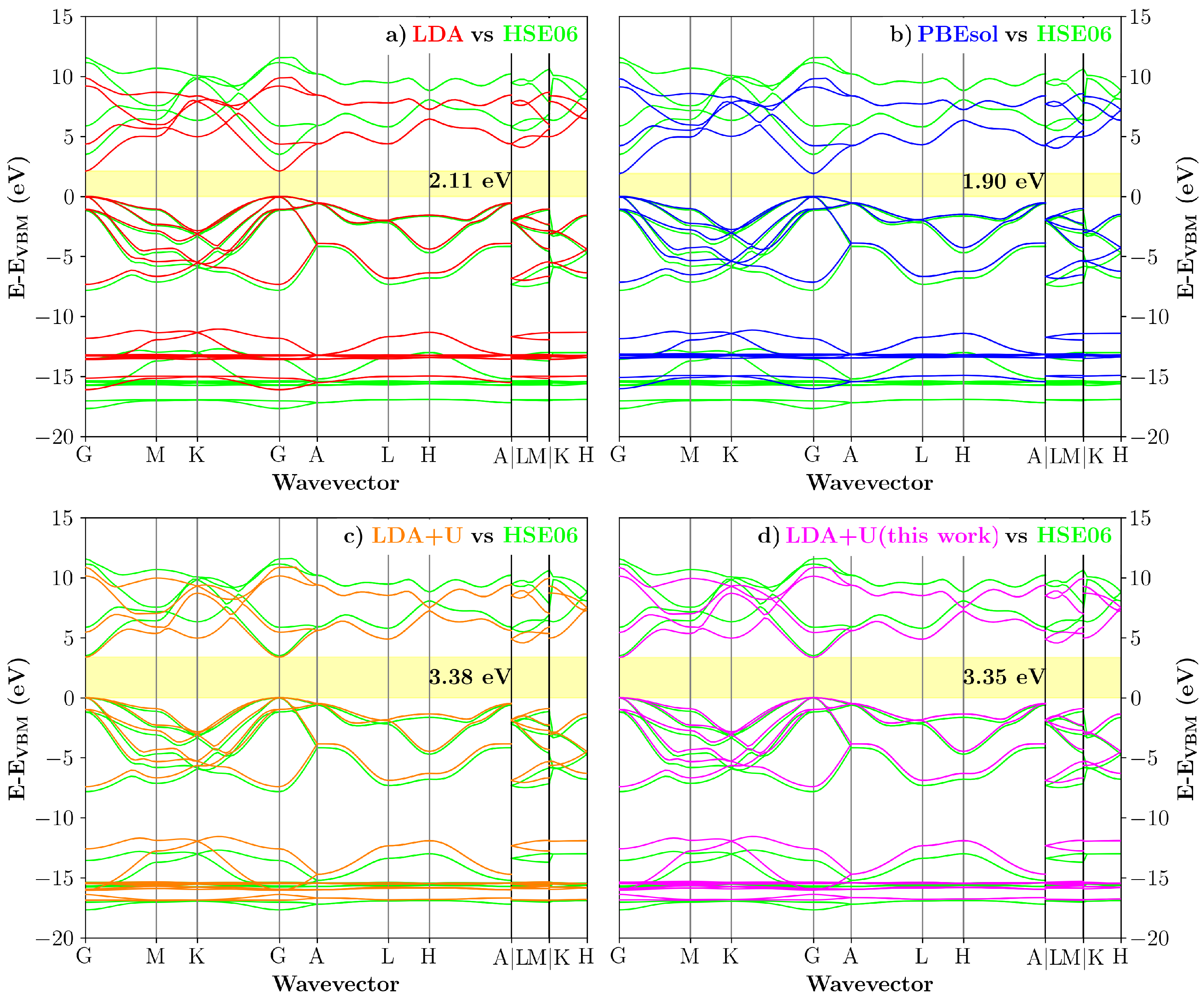
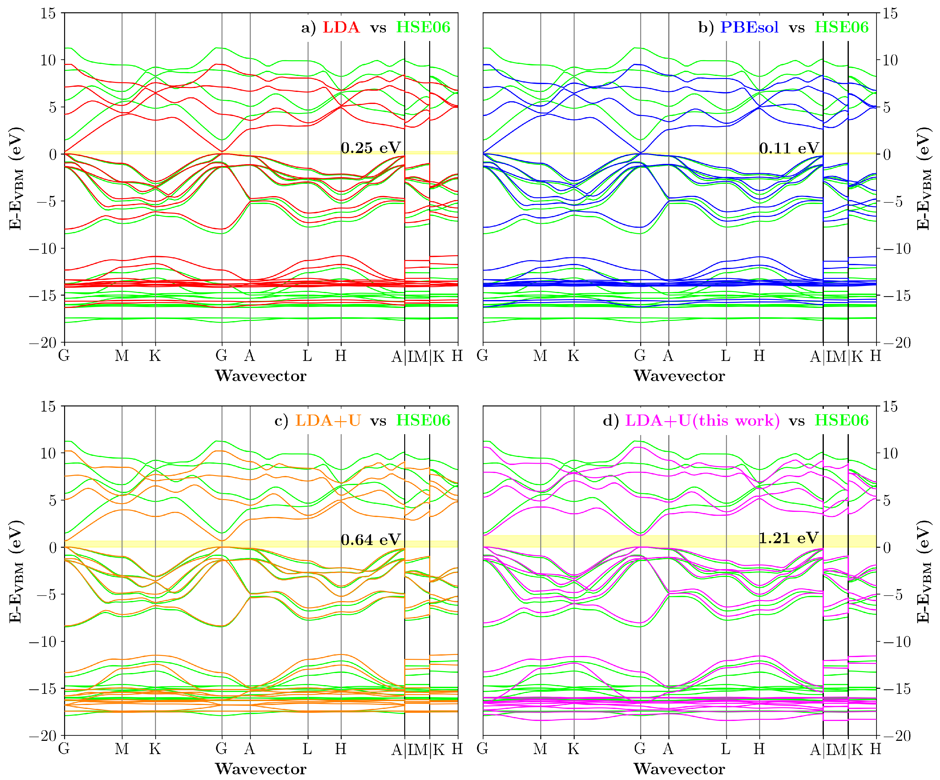
3.3. Transferability Check: 1:1 InN/GaN Superlattice
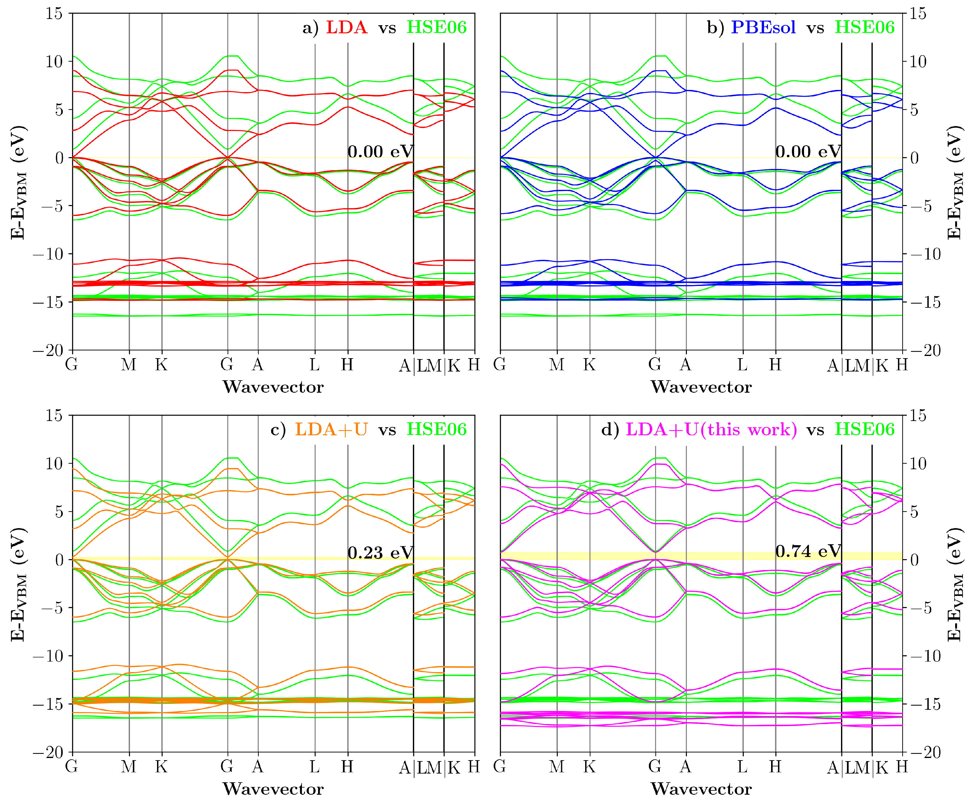
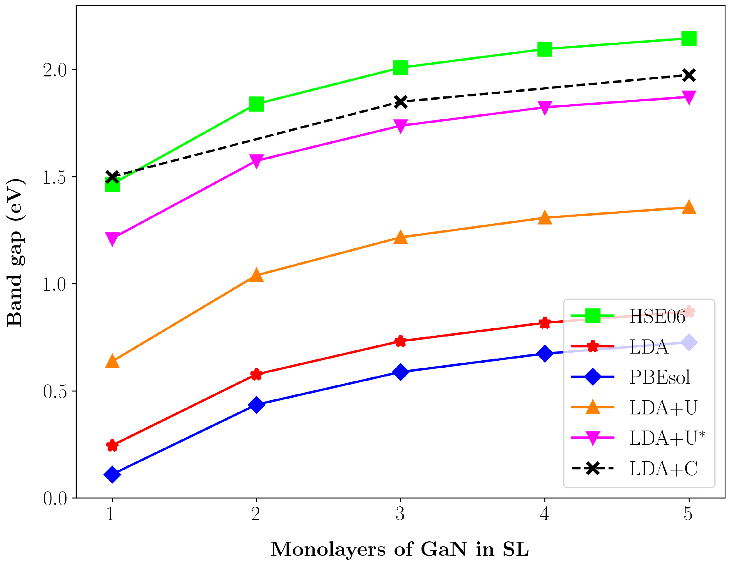
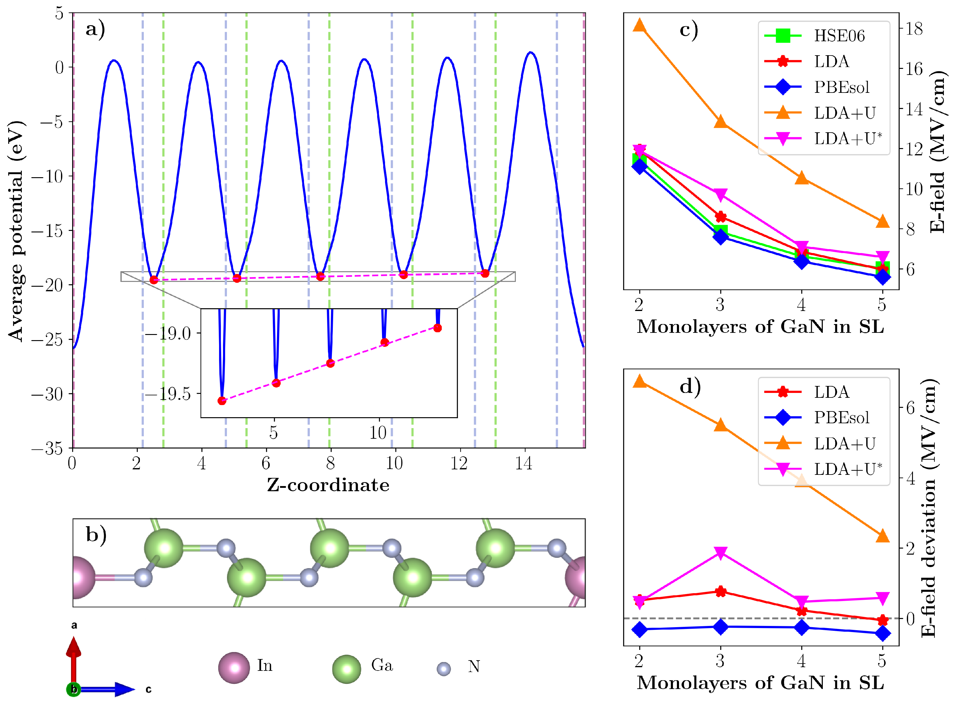
3.4. Internal Electric Fields in 1:2–5 InN/GaN Superlattices
4. Conclusions
Supplementary Materials
Author Contributions
Funding
Institutional Review Board Statement
Informed Consent Statement
Data Availability Statement
Acknowledgments
Conflicts of Interest
References
- Nakamura, S.; Senoh, M.; Nagahama, S.; Iwasa, N.; Yamada, T.; Matsushita, T.; Kiyoku, H.; Sugimoto, Y. InGaN-Based Multi-Quantum-Well-Structure Laser Diodes. Jpn. J. Appl. Phys. 1996, 35, L74–L76. [Google Scholar] [CrossRef]
- Tadatomo, K.; Okagawa, H.; Ohuchi, Y.; Tsunekawa, T.; Imada, Y.; Kato, M.; Taguchi, T. High Output Power InGaN Ultraviolet Light-Emitting Diodes Fabricated on Patterned Substrates Using Metalorganic Vapor Phase Epitaxy. Jpn. J. Appl. Phys. 2001, 40, L583–L585. [Google Scholar] [CrossRef]
- Kim, H.M.; Cho, Y.H.; Lee, H.; Kim, S.I.; Ryu, S.R.; Kim, D.Y.; Kang, T.W.; Chung, K.S. High-Brightness Light Emitting Diodes Using Dislocation-Free Indium Gallium Nitride/Gallium Nitride Multiquantum-Well Nanorod Arrays. Nano Lett. 2004, 4, 1059–1062. [Google Scholar] [CrossRef]
- Qian, F.; Li, Y.; Gradečak, S.; Park, H.G.; Dong, Y.; Ding, Y.; Wang, Z.L.; Lieber, C.M. Multi-quantum-well nanowire heterostructures for wavelength-controlled lasers. Nat. Mater. 2008, 7, 701–706. [Google Scholar] [CrossRef]
- Tan, C.K.; Tansu, N. Electrons and holes get closer. Nat. Nanotechnol. 2015, 10, 107–109. [Google Scholar] [CrossRef] [PubMed]
- Tsao, J.Y.; Crawford, M.H.; Coltrin, M.E.; Fischer, A.J.; Koleske, D.D.; Subramania, G.S.; Wang, G.T.; Wierer, J.J.; Karlicek, R.F. Toward Smart and Ultra-efficient Solid-State Lighting. Adv. Opt. Mater. 2014, 2, 809–836. [Google Scholar] [CrossRef]
- Farrell, R.M.; Young, E.C.; Wu, F.; DenBaars, S.P.; Speck, J.S. Materials and growth issues for high-performance nonpolar and semipolar light-emitting devices. Semicond. Sci. Technol. 2012, 27, 024001. [Google Scholar] [CrossRef]
- Zhao, H.; Liu, G.; Zhang, J.; Poplawsky, J.D.; Dierolf, V.; Tansu, N. Approaches for high internal quantum efficiency green InGaN light-emitting diodes with large overlap quantum wells. Opt. Express 2011, 19, A991. [Google Scholar] [CrossRef] [PubMed] [Green Version]
- Moses, P.G.; de Walle, C.G.V. Band bowing and band alignment in InGaN alloys. Appl. Phys. Lett. 2010, 96, 021908. [Google Scholar] [CrossRef]
- Miao, M.S.; Yan, Q.; Van de Walle, C.G.; Lou, W.K.; Li, L.L.; Chang, K. Polarization-Driven Topological Insulator Transition in a GaN/InN/GaN Quantum Well. Phys. Rev. Lett. 2012, 109, 186803. [Google Scholar] [CrossRef] [Green Version]
- Gorczyca, I.; Skrobas, K.; Suski, T.; Christensen, N.; Svane, A. Influence of strain and internal electric fields on band gaps in short period nitride based superlattices. Superlattices Microstruct. 2015, 82, 438–446. [Google Scholar] [CrossRef]
- Gorczyca, I.; Suski, T.; Strak, P.; Staszczak, G.; Christensen, N.E. Band gap engineering of In(Ga)N/GaN short period superlattices. Sci. Rep. 2017, 7. [Google Scholar] [CrossRef] [Green Version]
- Gorczyca, I.; Suski, T.; Christensen, N.E.; Svane, A. Theoretical study of nitride short period superlattices. J. Phys. Condens. Matter 2018, 30, 063001. [Google Scholar] [CrossRef] [Green Version]
- De Carvalho, L.C.; Schleife, A.; Furthmüller, J.; Bechstedt, F. Ab initio calculation of optical properties with excitonic effects in wurtzite InxGa1−xN and InxAl1−xN alloys. Phys. Rev. B 2013, 87, 195211. [Google Scholar] [CrossRef]
- Sun, W.; Tan, C.K.; Tansu, N. III-Nitride Digital Alloy: Electronics and Optoelectronics Properties of the InN/GaN Ultra-Short Period Superlattice Nanostructures. Sci. Rep. 2017, 7. [Google Scholar] [CrossRef] [PubMed] [Green Version]
- Pacchioni, G.; Frigoli, F.; Ricci, D.; Weil, J.A. Theoretical description of hole localization in a quartz Al center: The importance of exact electron exchange. Phys. Rev. B 2000, 63, 054102. [Google Scholar] [CrossRef]
- Hasnip, P.J.; Refson, K.; Probert, M.I.J.; Yates, J.R.; Clark, S.J.; Pickard, C.J. Density functional theory in the solid state. Philos. Trans. R. Soc. A Math. Phys. Eng. Sci. 2014, 372, 20130270. [Google Scholar] [CrossRef] [PubMed] [Green Version]
- Borlido, P.; Schmidt, J.; Huran, A.W.; Tran, F.; Marques, M.A.L.; Botti, S. Exchange-correlation functionals for band gaps of solids: Benchmark, reparametrization and machine learning. Npj Comput. Mater. 2020, 6. [Google Scholar] [CrossRef]
- Gerosa, M.; Bottani, C.E.; Valentin, C.D.; Onida, G.; Pacchioni, G. Accuracy of dielectric-dependent hybrid functionals in the prediction of optoelectronic properties of metal oxide semiconductors: A comprehensive comparison with many-bodyGWand experiments. J. Phys. Condens. Matter 2017, 30, 044003. [Google Scholar] [CrossRef] [PubMed]
- Janesko, B.G. Replacing hybrid density functional theory: Motivation and recent advances. Chem. Soc. Rev. 2021. [Google Scholar] [CrossRef]
- Christensen, N.E. Electronic structure of GaAs under strain. Phys. Rev. B 1984, 30, 5753–5765. [Google Scholar] [CrossRef]
- Anisimov, V.I.; Zaanen, J.; Andersen, O.K. Band theory and Mott insulators: Hubbard U instead of Stoner I. Phys. Rev. B 1991, 44, 943–954. [Google Scholar] [CrossRef] [Green Version]
- Dudarev, S.L.; Botton, G.A.; Savrasov, S.Y.; Humphreys, C.J.; Sutton, A.P. Electron-energy-loss spectra and the structural stability of nickel oxide: An LSDA+U study. Phys. Rev. B 1998, 57, 1505–1509. [Google Scholar] [CrossRef]
- Liechtenstein, A.I.; Anisimov, V.I.; Zaanen, J. Density-functional theory and strong interactions: Orbital ordering in Mott-Hubbard insulators. Phys. Rev. B 1995, 52, R5467–R5470. [Google Scholar] [CrossRef] [Green Version]
- Terentjevs, A.; Catellani, A.; Prendergast, D.; Cicero, G. Importance of on-site corrections to the electronic and structural properties of InN in crystalline solid, nonpolar surface, and nanowire forms. Phys. Rev. B 2010, 82, 165307. [Google Scholar] [CrossRef]
- Molina-Sánchez, A.; García-Cristóbal, A.; Cantarero, A.; Terentjevs, A.; Cicero, G. LDA+U and tight-binding electronic structure of InN nanowires. Phys. Rev. B 2010, 82, 165324. [Google Scholar] [CrossRef]
- De Carvalho, L.C.; Schleife, A.; Furthmüller, J.; Bechstedt, F. Distribution of cations in wurtzitic InxGa1−xN and InxAl1−xN alloys: Consequences for energetics and quasiparticle electronic structures. Phys. Rev. B 2012, 85, 115121. [Google Scholar] [CrossRef] [Green Version]
- Yu, M.; Yang, S.; Wu, C.; Marom, N. Machine learning the Hubbard U parameter in DFT+U using Bayesian optimization. Npj Comput. Mater. 2020, 6. [Google Scholar] [CrossRef]
- Frazier, P.I. A Tutorial on Bayesian Optimization. arXiv 2018, arXiv:1807.02811. [Google Scholar]
- Nogueira, F. Bayesian Optimization: Open Source Constrained Global Optimization Tool for Python. 2014. Available online: https://github.com/fmfn/BayesianOptimization (accessed on 2 August 2021).
- Kresse, G.; Hafner, J. Ab initio molecular dynamics for liquid metals. Phys. Rev. B 1993, 47, 558–561. [Google Scholar] [CrossRef]
- Kresse, G.; Hafner, J. Ab initio molecular-dynamics simulation of the liquid-metal–amorphous-semiconductor transition in germanium. Phys. Rev. B 1994, 49, 14251–14269. [Google Scholar] [CrossRef]
- Kresse, G.; Furthmüller, J. Efficiency of ab-initio total energy calculations for metals and semiconductors using a plane-wave basis set. Comput. Mater. Sci. 1996, 6, 15–50. [Google Scholar] [CrossRef]
- Kresse, G.; Furthmüller, J. Efficient iterative schemes for ab initio total-energy calculations using a plane-wave basis set. Phys. Rev. B 1996, 54, 11169–11186. [Google Scholar] [CrossRef] [PubMed]
- Kresse, G.; Joubert, D. From ultrasoft pseudopotentials to the projector augmented-wave method. Phys. Rev. B 1999, 59, 1758–1775. [Google Scholar] [CrossRef]
- Setyawan, W.; Curtarolo, S. High-throughput electronic band structure calculations: Challenges and tools. Comput. Mater. Sci. 2010, 49, 299–312. [Google Scholar] [CrossRef] [Green Version]
- Ceperley, D.M.; Alder, B.J. Ground State of the Electron Gas by a Stochastic Method. Phys. Rev. Lett. 1980, 45, 566–569. [Google Scholar] [CrossRef] [Green Version]
- Csonka, G.I.; Perdew, J.P.; Ruzsinszky, A.; Philipsen, P.H.T.; Lebègue, S.; Paier, J.; Vydrov, O.A.; Ángyán, J.G. Assessing the performance of recent density functionals for bulk solids. Phys. Rev. B 2009, 79, 155107. [Google Scholar] [CrossRef]
- Bengone, O.; Alouani, M.; Blöchl, P.; Hugel, J. Implementation of the projector augmented-wave LDA+U method: Application to the electronic structure of NiO. Phys. Rev. B 2000, 62, 16392–16401. [Google Scholar] [CrossRef] [Green Version]
- Rohrbach, A.; Hafner, J.; Kresse, G. Electronic correlation effects in transition-metal sulfides. J. Phys. Condens. Matter 2003, 15, 979–996. [Google Scholar] [CrossRef]
- Krukau, A.V.; Vydrov, O.A.; Izmaylov, A.F.; Scuseria, G.E. Influence of the exchange screening parameter on the performance of screened hybrid functionals. J. Chem. Phys. 2006, 125, 224106. [Google Scholar] [CrossRef] [PubMed]
- Saib, S.; Bouarissa, N. Structural phase transformations of GaN and InN under high pressure. Phys. B Condens. Matter 2007, 387, 377–382. [Google Scholar] [CrossRef]
- Dreyer, C.E.; Janotti, A.; Van de Walle, C.G.; Vanderbilt, D. Correct Implementation of Polarization Constants in Wurtzite Materials and Impact on III-Nitrides. Phys. Rev. X 2016, 6, 021038. [Google Scholar] [CrossRef]
- Lyons, J.L.; de Walle, C.G.V. Computationally predicted energies and properties of defects in GaN. Npj Comput. Mater. 2017, 3. [Google Scholar] [CrossRef]
- Kaczkowski, J. Electronic Structure of Some Wurtzite Semiconductors: Hybrid Functionals vs. Ab Initio Many Body Calculations. Acta Phys. Pol. A 2012, 121, 1142–1144. [Google Scholar] [CrossRef]
- Rasmussen, C. Gaussian Processes for Machine Learning; MIT Press: Cambridge, MA, USA, 2006. [Google Scholar]
- Vurgaftman, I.; Meyer, J.R. Band parameters for nitrogen-containing semiconductors. J. Appl. Phys. 2003, 94, 3675–3696. [Google Scholar] [CrossRef]
- Morales-García, Á.; Valero, R.; Illas, F. An Empirical, yet Practical Way To Predict the Band Gap in Solids by Using Density Functional Band Structure Calculations. J. Phys. Chem. C 2017, 121, 18862–18866. [Google Scholar] [CrossRef] [Green Version]
- Monemar, B.; Paskov, P.; Kasic, A. Optical properties of InN—The bandgap question. Superlattices Microstruct. 2005, 38, 38–56. [Google Scholar] [CrossRef]
- Eisele, H.; Schuppang, J.; Schnedler, M.; Duchamp, M.; Nenstiel, C.; Portz, V.; Kure, T.; Bügler, M.; Lenz, A.; Dähne, M.; et al. Intrinsic electronic properties of high-quality wurtzite InN. Phys. Rev. B 2016, 94, 245201. [Google Scholar] [CrossRef] [Green Version]
- Tsai, Y.C.; Bayram, C. Band Alignments of Ternary Wurtzite and Zincblende III-Nitrides Investigated by Hybrid Density Functional Theory. ACS Omega 2020, 5, 3917–3923. [Google Scholar] [CrossRef] [Green Version]
- Bi, Z.; Lenrick, F.; Colvin, J.; Gustafsson, A.; Hultin, O.; Nowzari, A.; Lu, T.; Wallenberg, R.; Timm, R.; Mikkelsen, A.; et al. InGaN Platelets: Synthesis and Applications toward Green and Red Light-Emitting Diodes. Nano Lett. 2019, 19, 2832–2839. [Google Scholar] [CrossRef]
- Gülink, J.; Bornemann, S.; Spende, H.; Maur, M.A.D.; Carlo, A.D.; Prades, J.D.; Wasisto, H.S.; Waag, A. InGaN/GaN nanoLED Arrays as a Novel Illumination Source for Biomedical Imaging and Sensing Applications. Proceedings 2018, 2, 892. [Google Scholar] [CrossRef] [Green Version]
- Liu, Y.; Hyun, B.R.; Wang, Y.; Zhang, K.; Kwok, H.S.; Liu, Z. R/G/B Micro-LEDs for In-Pixel Integrated Arrays and Temperature Sensing. ACS Appl. Electron. Mater. 2020, 3, 3–10. [Google Scholar] [CrossRef]
- Soopy, A.K.K.; Li, Z.; Tang, T.; Sun, J.; Xu, B.; Zhao, C.; Najar, A. In(Ga)N Nanostructures and Devices Grown by Molecular Beam Epitaxy and Metal-Assisted Photochemical Etching. Nanomaterials 2021, 11, 126. [Google Scholar] [CrossRef] [PubMed]
- Nötzel, R. InN/InGaN quantum dot electrochemical devices: New solutions for energy and health. Natl. Sci. Rev. 2017, 4, 184–195. [Google Scholar] [CrossRef]
- Zhang, H.; Min, J.W.; Gnanasekar, P.; Ng, T.K.; Ooi, B.S. InGaN-based nanowires development for energy harvesting and conversion applications. J. Appl. Phys. 2021, 129, 121103. [Google Scholar] [CrossRef]
- Lin, J.; Wang, W.; Li, G. Modulating Surface/Interface Structure of Emerging InGaN Nanowires for Efficient Photoelectrochemical Water Splitting. Adv. Funct. Mater. 2020, 30, 2005677. [Google Scholar] [CrossRef]
- Ganesh, V.; Pandikumar, A.; Alizadeh, M.; Kalidoss, R.; Baskar, K. Rational design and fabrication of surface tailored low dimensional Indium Gallium Nitride for photoelectrochemical water cleavage. Int. J. Hydrogen Energy 2020, 45, 8198–8222. [Google Scholar] [CrossRef]
- Chatterjee, U.; Park, J.H.; Um, D.Y.; Lee, C.R. III-nitride nanowires for solar light harvesting: A review. Renew. Sustain. Energy Rev. 2017, 79, 1002–1015. [Google Scholar] [CrossRef]


Publisher’s Note: MDPI stays neutral with regard to jurisdictional claims in published maps and institutional affiliations. |
© 2021 by the authors. Licensee MDPI, Basel, Switzerland. This article is an open access article distributed under the terms and conditions of the Creative Commons Attribution (CC BY) license (https://creativecommons.org/licenses/by/4.0/).
Share and Cite
Popov, M.N.; Spitaler, J.; Romaner, L.; Bedoya-Martínez, N.; Hammer, R. Bayesian Optimization of Hubbard U’s for Investigating InGaN Superlattices. Electron. Mater. 2021, 2, 370-381. https://doi.org/10.3390/electronicmat2030025
Popov MN, Spitaler J, Romaner L, Bedoya-Martínez N, Hammer R. Bayesian Optimization of Hubbard U’s for Investigating InGaN Superlattices. Electronic Materials. 2021; 2(3):370-381. https://doi.org/10.3390/electronicmat2030025
Chicago/Turabian StylePopov, Maxim N., Jürgen Spitaler, Lorenz Romaner, Natalia Bedoya-Martínez, and René Hammer. 2021. "Bayesian Optimization of Hubbard U’s for Investigating InGaN Superlattices" Electronic Materials 2, no. 3: 370-381. https://doi.org/10.3390/electronicmat2030025
APA StylePopov, M. N., Spitaler, J., Romaner, L., Bedoya-Martínez, N., & Hammer, R. (2021). Bayesian Optimization of Hubbard U’s for Investigating InGaN Superlattices. Electronic Materials, 2(3), 370-381. https://doi.org/10.3390/electronicmat2030025