1. Introduction
Perovskite oxide ferroelectrics are known to exhibit excellent electro-mechanical properties that makes these materials major piezoelectrics [
1,
2]. Numerous piezoelectric applications of ferroelectric ceramics and crystals are commercialized and being continuously developed. Beyond this mainstream technology, modern sustainability requirements as well as demands for micro- and nanoscale devices stimulate advancement of piezoelectric thin films, which are free of hazardous elements such as lead and niobium [
3] and only a few to less than one micron in thickness. Moreover, for many applications it is crucial that piezoelectric strain-electric field behavior is free of hysteresis. Such hysteresis is typical for ferroelectrics and originates from the presence of domains with different orientations of spontaneous polarization. A certain coercive field is required to switch polarization, that leads to polarization—electric field hysteresis. Consequently, the dielectric permittivity and piezoelectric coefficient exhibit hysteresis in their field-dependent behavior.
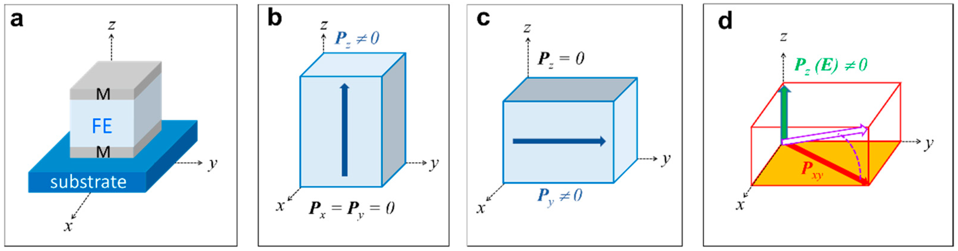
It is worth noting that compared to ceramics, domain configuration of thin films strongly depends on elastic coupling between a film and an underlying substrate. For a vertical stack of a tetragonal ferroelectric film sandwiched between electrodes (metal layers) and grown on top of a crystal substrate (
Figure 1a), there are two limiting cases of domains:
c-type domains, where polarization direction is aligned normal to the substrate surface, or in the out-of-plane direction (
Figure 1b), and
a-type domains, where polarization direction is aligned parallel to the substrate surface, or in the in-plane direction (
Figure 1c). For many ferroelectric materials, piezoelectric out-of-plane deformation is larger in the
c-type films than in the
a-type ones when electric field is applied in the out-of-plane direction (
Figure 1a). Whereas epitaxial
c-type films allow for maximizing piezoresponse magnitude, switching of the 180°
c-domains produces strong hysteresis therein. The presence of
a-type domains diminishes coercive field (voltage) at the expense of response magnitude. Therefore, engineering domain configuration is one of the tools for tailoring piezoelectric properties of thin films.
In recent decades, control of domain configuration was extensively studied in epitaxial ferroelectric films. By using a substrate, whose lattice parameters are smaller than those of a ferroelectric material, a biaxial in-plane compressive misfit strain can be imposed on the film and stimulate the formation of
c-domains therein. Correspondingly, to enforce in-plane polarization, a tensile substrate should be employed. The type, width, and spatial distribution of different domains result from a delicate interplay between misfit strain, thickness of the film, and properties of the film’s material [
4]. Practical implementation of this fascinating approach is, unfortunately, restricted by selection of appropriate substrates, which may be too expensive, difficult to synthesize, or unavailable in reality.
Here, we demonstrate that, instead of the film-substrate lattice misfit, a film-substrate mismatch in the coefficients of thermal expansion (CTE) can be effectively used to manage domains and achieve hysteresis-free piezoresponse. Synthesis of perovskite-structure ferroelectric films requires high temperatures of 800–1200 K. During cooling from the synthesis (deposition) temperature, the CTE mismatch causes a build-up of a thermal strain in the films. The linear CTE values are positive and typically (0.6–1.5) × 10
−5 K
−1 in the high-temperature cubic paraelectric phase of many ferroelectrics, about (0.7–1.3) × 10
−5 K
−1 in common oxide substrates, and as small as 0.26 × 10
−5 K
−1 at 300 K and 4.2 × 10
−5 K
−1 at 1000 K in silicon, which is the main commercial substrate material [
5,
6,
7,
8,
9,
10]. These coefficients ensure possibility for tensile thermal-mismatch strain (or thermal strain here for brevity) in ferroelectric films. Moreover, this strain can be continuously varied by altering deposition temperature [
11].
Here we focus on archetypical, environmentally friendly, biocompatible, and low-cost ferroelectric BaTiO
3 (BTO), which is a basis for sustainable piezoelectrics [
12]. To enable epitaxial growth and thermal tension, we employed research SrTiO
3 (STO) substrates. The BTO/STO compressive misfit strain is large and relaxes during deposition, whereas tensile thermal strain builds up on cooling [
13,
14]. The thermal tension produces an
r-type phase, where spontaneous polarization is in-plane and where an out-of-plane polarization can be induced by the application of out-of-plane electric field. The total polarization rotates toward the out-of-plane direction (
Figure 1d). Using this mechanism, nearly hysteresis-free polarization was previously achieved in 200–400 nm thick films [
13]. Here we report on hysteresis-free piezoresponse in the thermally strained BTO films with thickness of ~1 μm. The films possess effective piezoelectric coefficient to ~50 pm/V and exhibit linear strain-field behavior. We anticipate that the demonstrated effect can be valid also for thin films grown on commercial silicon substrates.
2. Materials and Methods
Thin films of BTO and SrRuO
3 (SRO) bottom electrode were grown by pulsed laser deposition (PLD) using a KrF excimer laser (energy density ~2 J/cm
2) at a substrate temperature of 973 K and a pressure of ambient oxygen of 20 Pa. Postdeposition cooling was conducted at a rate of 5 K/min. Epitaxially polished (001) STO substrates were purchased from MTI Corporation. The thickness of the films was controlled by number of laser pulses and measured on a KLA-Tencor Alpha-Step IQ Surface Profilometer (KLA Instruments, Milpitas, CA, USA) using a step, which was formed by shadow masking during PLD. Concurrently, the surface roughness of the films was inspected using this Profilometer. The crystal structure of the films was characterized by X-ray diffraction on D8 DISCOVER diffractometers (Bruker corporation, Berlin, Germany) using Cu Kα radiation. More details on structural and morphological characterization can be found elsewhere [
13,
14]. Cube-on-cube growth and in-plane tensile strain in BTO were confirmed by θ–2θ scans and reciprocal space mapping (
Supplementary Figure S1).
For electrical and piezoelectric characterization, capacitor stacks were formed using circular top Pt contact pads (diameter 2 mm), created by room-temperature vacuum PLD of Pt through a shadow mask. To ensure high accuracy of double beam interferometric measurements of piezoresponse, the thickness of the optically reflecting top Pt electrodes was 60 nm. Back sides of the substrates were polished, and a highly reflecting Au layer was deposited thereon by PLD and sputtering. To safeguard reliable adhesion and stability of the backside reflecting layer, a thin PLD-prepared layer of Au was introduced prior to sputtering.
The quasi-static and dynamic polarization–voltage loops, leakage current, dynamic out-of-plane elongation–voltage loops, capacitance–bias curves, and effective piezoelectric coefficient–bias curves were measured on a double beam laser interferometer DBLI (aixACCT Systems GmbH, Aachen, Germany) equipped with a TF 2000 E Analyzer (aixACCT Systems GmbH, Aachen, Germany). For the measurements of capacitance and effective piezoelectric coefficient, the biasing dc voltage was superimposed with small ac voltage and swept from zero to a maximum positive, maximum negative, and back to zero voltages. In all measurements, the electric field was applied and the responses were acquired in the out-of-plane direction.
3. Results and Discussion
It was shown before that thermal tension enforces polarization to stay in-plane (
Figure 1d) in the BTO films on STO [
13,
14]. Such a phase was predicted theoretically and is characterized by the two in-plane polarization components being non-zero [
15,
16,
17]. The out-of-plane spontaneous polarization is zero, and the out-of-plane polarization-voltage curve is expected to be linear. However, the applied electric field induces a non-zero out-plane polarization component and thus causes a transformation to another,
r-type phase, which was also predicted theoretically. The total polarization rotates out from the in-plane location under the applied field (
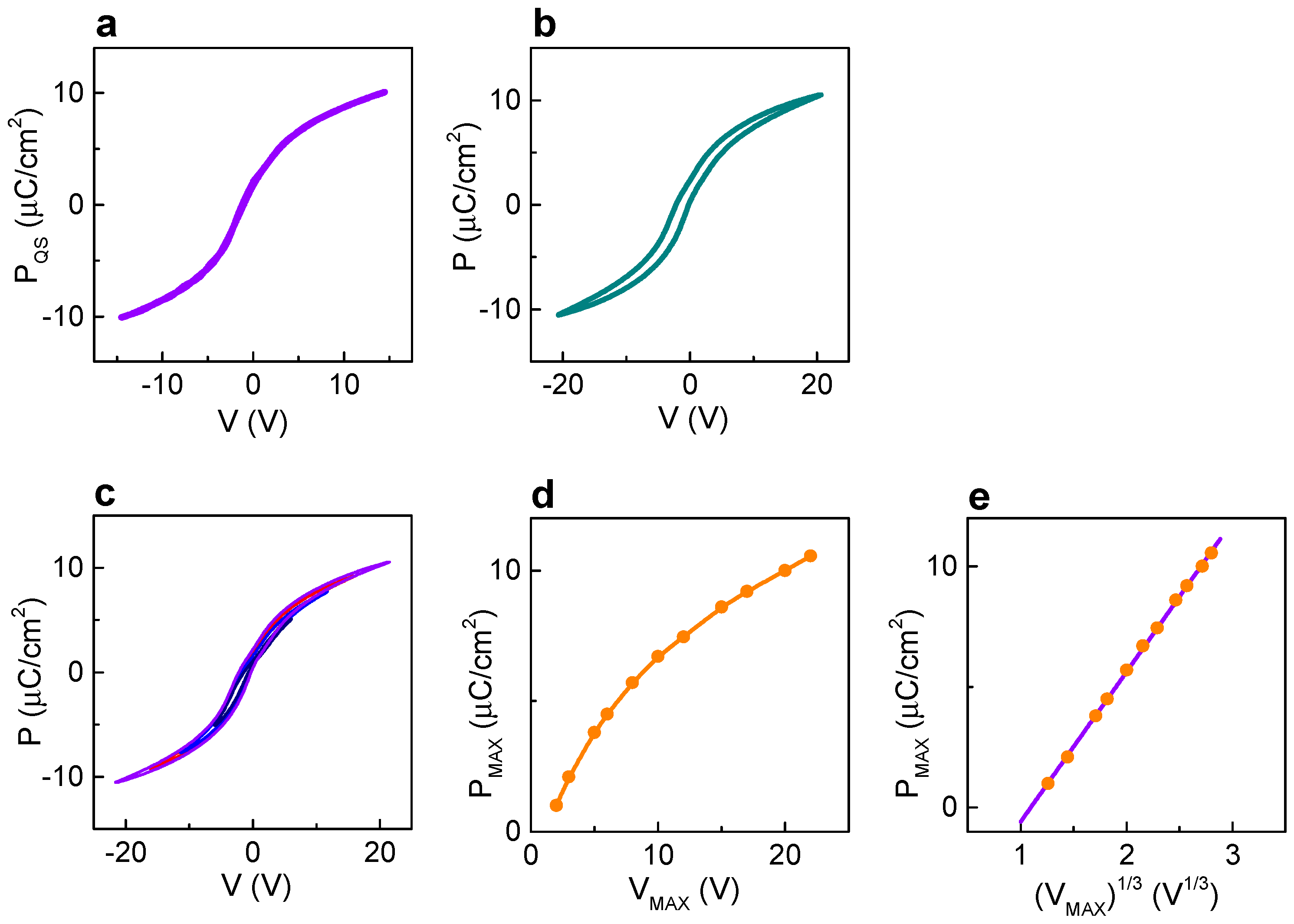
Figure 1d) and turns back when the field is switched off. Correspondingly, the measured quasi-static polarization-voltage curve is not linear. Because polarization rotations are nearly instantaneous, there is no remnant polarization. The hysteresis-free quasi-static polarization–voltage loop was obtained previously and is perfectly reproduced here (
Figure 2a).
Consistent with this behavior, also the dynamic polarization—voltage (P–V) loop is very slim and practically hysteresis-free (
Figure 2b). We note that slim P–V loops are measured at all magnitudes of maximum applied voltage V
MAX (
Figure 2c and
Supplementary Figures S2 and S3), that is in striking contrast to regular ferroelectric loops with the Rayleigh-type shape at small sub-switching voltages. The maximum polarization P
MAX increases with increasing maximum voltage V
MAX (
Figure 2c,d). The scaling behavior (P
MAX ∞ (V
MAX)
1/3) is evidenced by a good linear fit in
Figure 2e. This polarization-voltage scaling also agrees with our previous observations of polarization rotation [
13].
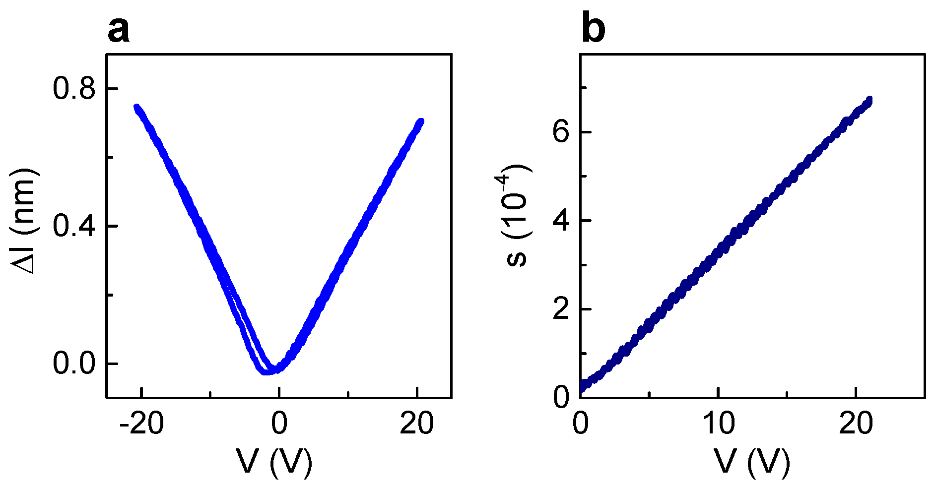
From the hysteresis-free polarization behavior (
Figure 2), it is easy to understand the lack of hysteresis in the voltage dependence of the out-of-plane elongation ∆l (
Figure 3a). Remarkably, the strain-voltage characteristic is perfectly linear (
Figure 3b), which is often desirable but seldom achievable.
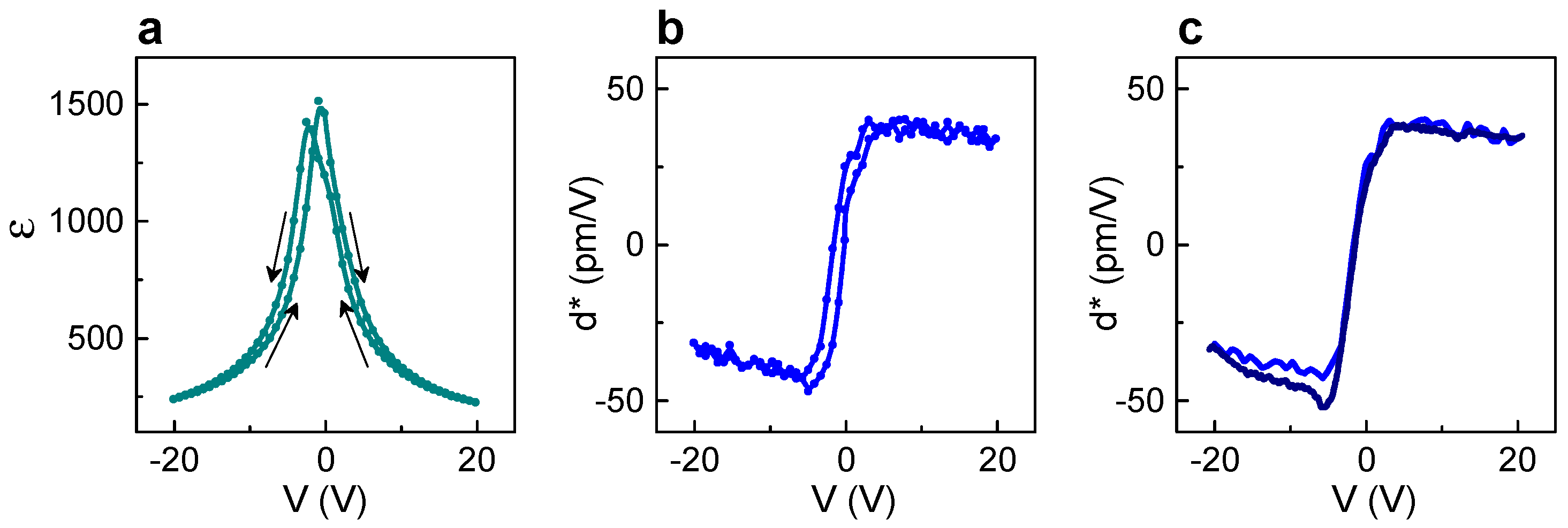
We note that dynamic characteristics (
Figure 2 and
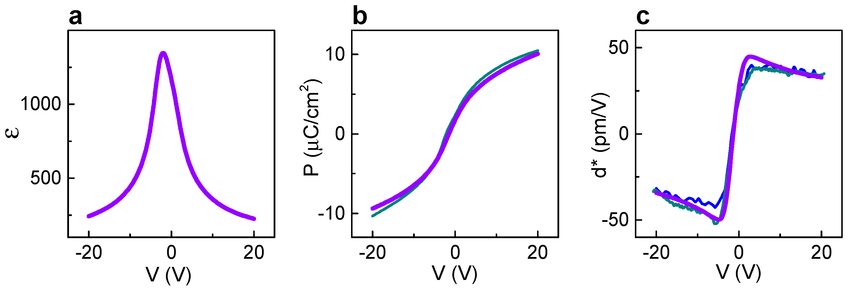
Figure 3) are measured by applying a sine voltage of a certain amplitude, which can significantly exceed coercive voltage. Such measurements are impossible for bulk samples and, strictly speaking, their results cannot be immediately apprehended from the common point of view. Another, more conventional approach is to use a small ac voltage and superimpose a biasing dc voltage. For convenience, we denote this regime as “static” here. The real part of the dielectric permittivity, ε, and the effective piezoelectric coefficient, d*, which were measured in the static regime, are presented in
Figure 4a,b, correspondingly. Only minor hysteresis is observed for different directions of the bias sweeps in the (ε–V) behavior (
Figure 4a), consistent with the slim dynamic (P–V) loops (
Figure 2b). Correspondingly, also hysteresis in the (d*–V) behavior is minute. To relate the results obtained in the two different regimes, the dynamic effective coefficient d* was extracted by differentiating the strain–voltage data (
Figure 3a). There is a perfect agreement between the extracted dynamic coefficient and the static one (
Figure 4c).
The maximum achieved magnitude of d* is 50 pm/V, which coincides with the results of the truly static measurements using x-ray diffraction analysis [
18]. It is worth emphasizing that piezoelectric coefficients reported for thin films are usually determined from dynamic responses of thin-film devices, or using piezoresponse force microscopy (PFM), or using single-beam interferometry. These methods are not free from significant uncertainties related to device modeling, PFM calibration, or substrate contribution. Here, the double-beam interferometry in combination with the specially prepared optically reflecting layers of the top surfaces of the films and on the back-side surfaces of the substrates ensured high accuracy for the effective piezoelectric coefficient.
To get a further insight into the observed nearly linear and hysteresis-free piezoelectric behavior, we calculated the polarization and the piezoelectric coefficient using the measured dielectric permittivity. For the ascending voltage branch of the (ε—V) sweep (
Figure 4a and
Figure 5a), the polarization–voltage curve was obtained by integration as
P = ε
0 ∫ ε (V)dV (
Figure 5b). Here, ε
0 is the permittivity of vacuum. The piezoelectric coefficient was then estimated as d* = 2
Q ε
0 ε
P, where
Q = 0.1 m
2/C
2 is the coefficient of electrostriction of BTO [
19]. The calculated piezoelectric coefficient is in excellent agreement with the measured ones (
Figure 5c).
The obtained direct dielectric–piezoelectric link implies a negligible, if any, role of spontaneous polarization in the out-of-plane piezoresponse. This behavior is very unusual, but comprehensible from the field-induced polarization as illustrated in
Figure 1d. We note that the
r-type phase in the film cannot be straightforwardly compared with any of the phases in bulk BTO (i.e., tetragonal, orthorhombic, and rhombohedral). Therefore, the achieved large permittivity and piezoelectric coefficient cannot be assigned and indexed in accordance with common BTO notations. An appropriate theoretical thermodynamic potential should be developed for predictive theoretical modeling of piezoelectric behavior in the
r-films. Finally, it is worth mentioning that the CTE mismatch between BTO and Si is very large. This mismatch suggests that profound thermally induced tensile strain can be created and used to tailor hysteresis-free and linear piezoresponse in BTO films on commercial substrates.
4. Conclusions
Polarization, dielectric permittivity, and piezoelectric response were experimentally investigated as a function of applied voltage under dynamic and quasi-static conditions in thin-film stack of archetypical, environmentally friendly, biocompatible, and low-cost ferroelectric BaTiO3, sandwiched between electrodes and grown on top of SrTiO3 substrate. High accuracy of piezoelectric characterization was ensured by double beam interferometric technique.
The measured out-of-plane quasi-static response functions were found to be free of hysteresis, and only a minute hysteresis was observed in the dynamic responses. The static and dynamic effective piezoelectric coefficients agreed with each other and amounted to ~50 pm/V. Concurrently, the strain-field dependence was found to be linear. A direct link between the dielectric permittivity and piezoelectric coefficient was established, discarding spontaneous polarization as contributing to the out-of-plane piezoresponse. The observations were consistent with the out-of-plane field induced polarization, whereas spontaneous polarization was in-plane due to in-plane tensile thermal strain. It was anticipated that hysteresis-free linear piezoresponse can be achieved in thin films on commercial silicon substrates, which enable large thermal strain.


