Article

Low-Cost Nanostructured Thin Films as Covert Laser Readable Security Tags for Large-Scale Productions Tracking

1
COMATEC Institute, School of Management and Engineering Vaud—HEIG-VD, HES-SO University of Applied Sciences and Arts Western Switzerland, 1401 Yverdon-les-Bains, Switzerland
2
School of Engineering—HE-Arc Ingénierie, HES-SO University of Applied Sciences Western Switzerland, 2000 Neuchâtel, Switzerland
*
Author to whom correspondence should be addressed.
Appl. Nano 2021, 2(4), 319-329; https://doi.org/10.3390/applnano2040023
Submission received: 1 August 2021 / Revised: 5 September 2021 / Accepted: 5 October 2021 / Published: 29 October 2021

Abstract

:
We report here the feasibility study of anti-counterfeiting low-cost nanostructured flexible security tags for the tracking of large-scale fabrication products, such as pharmaceuticals or original equipment manufacturers. The fabrication process makes use of the mature nanotechnology called Template Synthesis to shape thin track-etched polymer film into covert laser readable tags, combining random self-organized structures with organized patterns. Techniques are developed to drastically limit the number of fabrication steps and keep fabrication costs low, while opening to numerous adjustment parameters. A dedicated, simple optical setup is presented, to capture speckle images of such tags lightened up by light emitting diodes or laser beams. Speckle images are analyzed in terms of encoding parameters, found here quite numerous to ensure a large coding range of large-scale production batches. We particularly highlight ultra-dark areas in speckle images, where nanowire structures completely inhibit speckle patterns. This unique, high-contrast optical feature addresses these low-cost nanostructured thin films to provide a very promising solution for large-scale security tags.

1. Introduction

To combat counterfeiting, companies producing large-scale industrial products, such as pharmaceuticals or original equipment manufacturers (OEMs) [1], are in high demand for increasingly secure traceability solutions for their products. As such, logos, barcodes, certificates of authenticity, radio frequency identification (RFID) chips, quick response codes (QR-codes) are part of the classic strategies for tracking products, with varying degrees of security.
A more specific security strategy is to provide the surface of the product with specific microstructures that can be searched by simple optical reading: holograms or iridescent areas of bank cards or banknotes are common examples. However, tampering techniques already make it possible to bypass these simple security tests. To increase the degree of safety, “invisible” optical techniques are implemented: the surfaces are micro- or nano-structured and are only searchable with specific techniques such as ultra-violet lights or laser beams.
Covert laser readable (CLR) surface structures are thus in great demand, because they allow the reveal of a complex “secret” with a simple laser pointer: a coherent laser light reflected by a given surface induces specific speckle images easy to capture. Speckle features then reveal the physical structure of the surface, with the immense advantage that the lower their structural resolution, the larger the speckle’s resolution: the laser beam is thus like a microscope that easily “reads” structures at micro- to nano-metric scales.
The most current CLR structures are the “security holograms” [2,3,4], which have a repetitive surface pattern giving the laser reflection the form of images or holographic texts easily readable to the naked eye. However, these holographic CLR structures are produced by relatively expensive lithographic techniques and are mainly aimed at the traceability of small series of products with high added value, in the field of watchmaking for example.
However, there is currently no practical CLR structures available for very large series productions such as pharmaceuticals or OEM parts, since they must meet three rigorous criteria:
  • Their cost must be marginal in the price of the product;
  • Identification must be simple, fast and cheap;
  • Adjustable fabrication parameters must be fairly numerous to allow a precise coding of the different batches.
This work presents the fabrication feasibility study of a low-cost, easily readable, self-organized nanostructured CLR flexible tags (hereafter called n-CLRs) with numerous adjustable parameters, which fulfill the above criteria. The fabrication process is first detailed, which makes use of the mature, cost-effective template synthesis nanotechnology to shape a polymer thin film into n-CLRs. An optical device is then described, which captures speckles images of randomly organized n-CLR surfaces. These latter are finally analyzed in terms of adjustable parameters.
The novelty of this work is the original fabrication process, close to those used by the printed circuit board (PCB) industry, which (i) drastically limits the fabrication steps number, and thus keeps fabrication costs low; and (ii) allows a large number of adjustable parameters for coding.

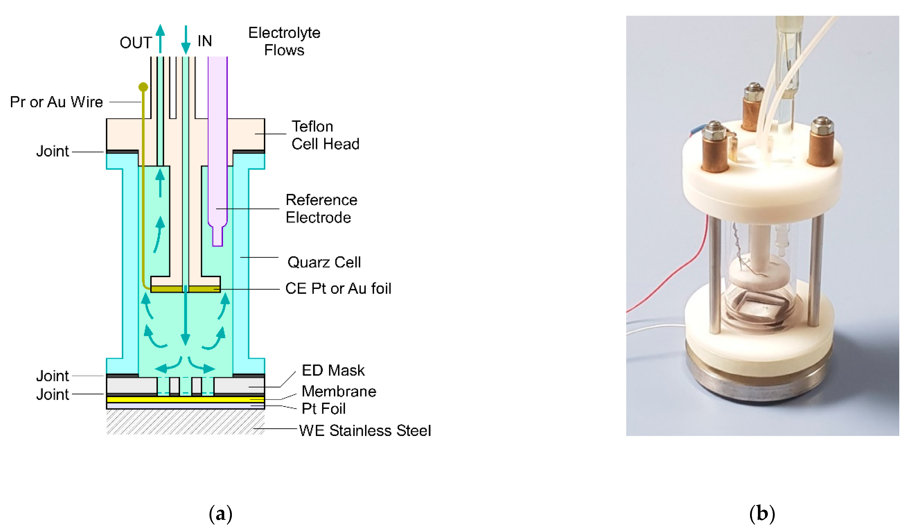
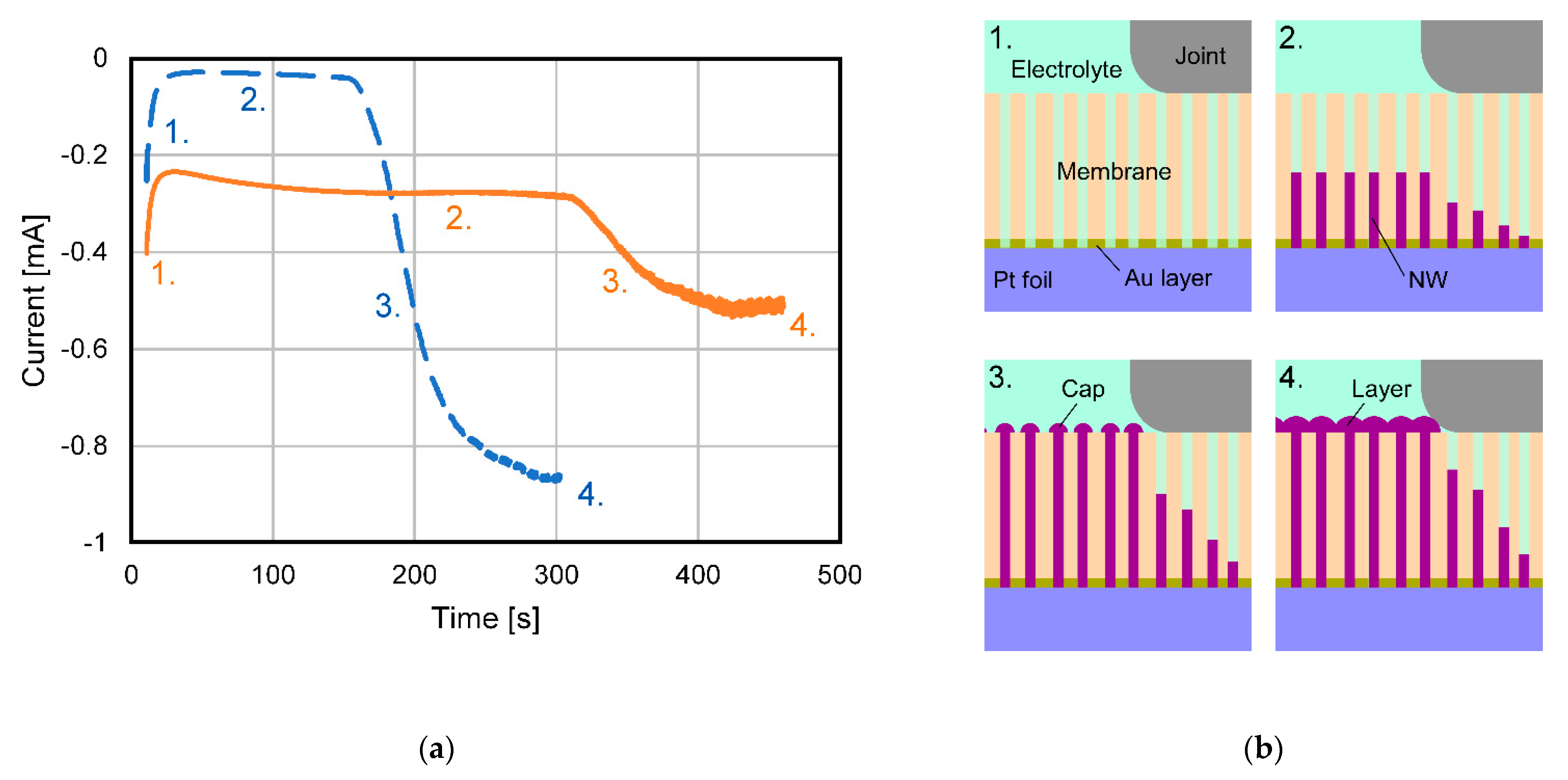
2. Materials and Methods

The starting materials for n-CLR fabrication are hydrophilic nanoporous polymer thin films, hereafter called membranes, nanostructured by the mature track-etch technology [5]. The most usual polymers for track-etched membranes are polycarbonate (PC), polyimide (PI) and polyethylene terephthalate (PET). The adjustable parameters are:
  • Polymer materials: PC, PI and PET;
  • Film thickness, ranging from 6 to 50 µm;
  • Pore diameter, down to 10 nm;
  • Pore density, from a few 109 pores/cm2 down to single pore structures [6].
The n-CLRs presented in this paper are made with the track-etched membranes detailed in Table 1, purchased from the company it4ip™ [7]. Note that commercial filter PC membranes from Millipore™ were also successfully tested for n-CLRs (not presented in this paper).
The first processing step is to sputter a gold layer of about 50 nm on one side of the membrane by the conventional physical vapor deposition (PVD) technique, under shadow masks if needed. Our sputtering device is a Leica EM SCD050. This is the only lithographic step of the process.
The second processing step is to fill up the pores by the template synthesis technique [8,9], i.e., by an electrochemical deposition of metal into the pores. A conventional Ni electrolyte solution was used to this purpose, analytically prepared at room temperature in deionized water (15.0 MΩ∙cm) by dissolution of 46.00 g/L boric acid (H3BO3—Carlo Erba, Analytics, ISO, ACS, Reag.Ph.Eur, Reag.USP), and then 256.44 g/l of nickel sulphate heptahydrate (NiSO4●7H2O—Sigma Aldrich,—purum p.a., crystalite, ≥99.0%). The Ni solution is constantly stirred under N2 bubbling in a 0.5 L tank maintained at 30.0 °C. The Ni solution was chosen for the sake of simplicity. Other materials can also be used for template synthesis of n-CLRs, like Cu or Cu-based alloys [10], in order to monitor (i) the optical reflectivity of n-CLR structures and (ii) their toxicity in terms of waste environmental impact.
The electrodeposition (ED) itself was performed in a dedicated cell presented in Figure 1. All the structure is mechanically pressed to make it water tight. A peristaltic pump forces the electrolyte to flow at about 60 mL/min from the 0.5 L tank into the cell, and back to the tank in a close loop. The gold layer sputtered on the membrane is electrically contacted to the working electrode (WE), via a platinum foil which insures the chemical passivity of the WE. The counter-electrode (CE) is a gold or platinum foil facing the membrane, with an opening in its center to let the electrolyte flow into the cell. An Ag/AgCl reference electrode (RE) is immersed in the electrolyte. The electrolyte bathes the membrane through an ED mask which patterns the aera where the ED will occur. This configuration imposes the ED of Ni to occur only through the pores uncovered by the ED mask.
ED masks are made out of polyoxymethylene (POM) 1 mm in thickness, and processed either by computer numerical control (CNC) machining or laser cut. It is patterned for this work in a 4 × 4 disks array, disks of 300 µm in diameter each, and 1 mm apart center-to-center from each other. The watertightness is insured by NBR joints. The joint in contact with the membrane is cut by laser with the same pattern than the ED mask. With this fast-prototyping technique, the average pattern resolution is about 30 µm, mainly imposed by the laser cut of the joint. Processing ED masks and nitrile rubber (NBR) joints by CNC techniques improves the resolution down to at least 5 µm. Nevertheless, the main advantage of the ED masks technique is to limit the electrochemical process at one single step, skipping conventional but expensive ultra-violet (UV) lithographic steps, such as resist coating, UV light exposure, resist development, seed layer sputtering and resist rincing [11].
The deposition of Ni is performed in potentiostatic mode with an Autolab PCSTAT204 device. Since the diameter and the length of the pores strongly limit the diffusion of Ni ions, a cyclic voltammetry has to be performed on each type of membrane to identify its working ED voltage V E D . Thus, typical ED voltages of −1.33 V and −1.25 V was set, respectively, for membranes A and B.
Examples of chronoamperometric curves are presented in Figure 2a, for membranes A (full line) and B (dotted line), both performed at V E D = 1.25 V, with the ED masks. The features of these curves are typical of such a template synthesis process: first a strong decrease in the current induced by the pores closing (Figure 2(b1,b2), then a plateau indicating that the pores are getting filled (Figure 2(b2)), until the inflexion point when the growth front reaches the surface of the membrane (Figure 2(b3)). The following current increase corresponds to the hemispherical overgrowth at the surface, until saturation when hemispheres overlap to reach a continuous growth surface (Figure 2(b4)). The pores filled with Ni are hereafter called nanowires (NWs).
To notice here the residual growth of NWs around the open ED area, due to the relatively poor tightness of the joint at its border. The electrolyte is then able to wet the membrane over an area about 100–200 µm broad below the joint. As it will be seen later in this paper, this feature is of great importance for the optical properties of n-CLRs.
The difference of pore density is depicted in Figure 2a by two main features: (i) the plateau currents which depend on the pore density, i.e., proportional to the growth front surface into the pores; and (ii) the ratio between the final saturation current and the plateau’s current, also expresses the change of the growth front surface between the pores and the overall surface.
The difference of saturation currents indicates the number of the 4 × 4 n-CLR effectively filled up with NWs: the larger it is, the more n-CLRs experienced a NWs’ growth. Therefore, Figure 2a shows that membrane A was less effective n-CLRs than membrane B.
It was observed that such an inhibition of ED occurred when air bubbles accidentally remained in the ED masks openings. This problem was solved by wetting the ED mask with deionized water before mounting the ED cell.
An easy way to access the nanometric features of n-CLRs is to illuminate it with a laser light and capture the image of their speckles, i.e., their diffractive interference pattern. This was achieved with the optical setup, presented in Figure 3, and all optical parts are listed in Table 2. The n-CLRs can be lit up either by an LED or by a laser, with respective wavelengths of 625 nm and 635 nm. A conventional telecentric lens system allows the LED to illuminate the n-CLRs in confocal mode, as well as focusing the reflected light to a charge-coupled device (CCD) camera. A polarized beam splitter coupled to a quarter waveplate suppressed the spurious reflection of the LED light on lenses 2 and 3. Focal lengths of lenses 1, 2 and 3 are respectively 10 mm, 80 mm and 16 mm. The iris diaphragm allowed the adjustment of the speckle size and number. The laser module illuminates the n-CLRs in direct mode with an incidence angle of about 45°. The n-CLRs were installed on a XYZ stage, which allowed along the Z-axe to focus n-CLR images to the camera, as well as to displace along the XY axes the membrane in order to scroll the 4 × 4 n-CLRs in the camera field.
The advantage of combining LED and laser lighting modes with a telecentric lens system is to obtain both the physical structure (shape, defects) image and the speckle patterns of n-CLRs, as detailed in Section 3.2.

3. Results

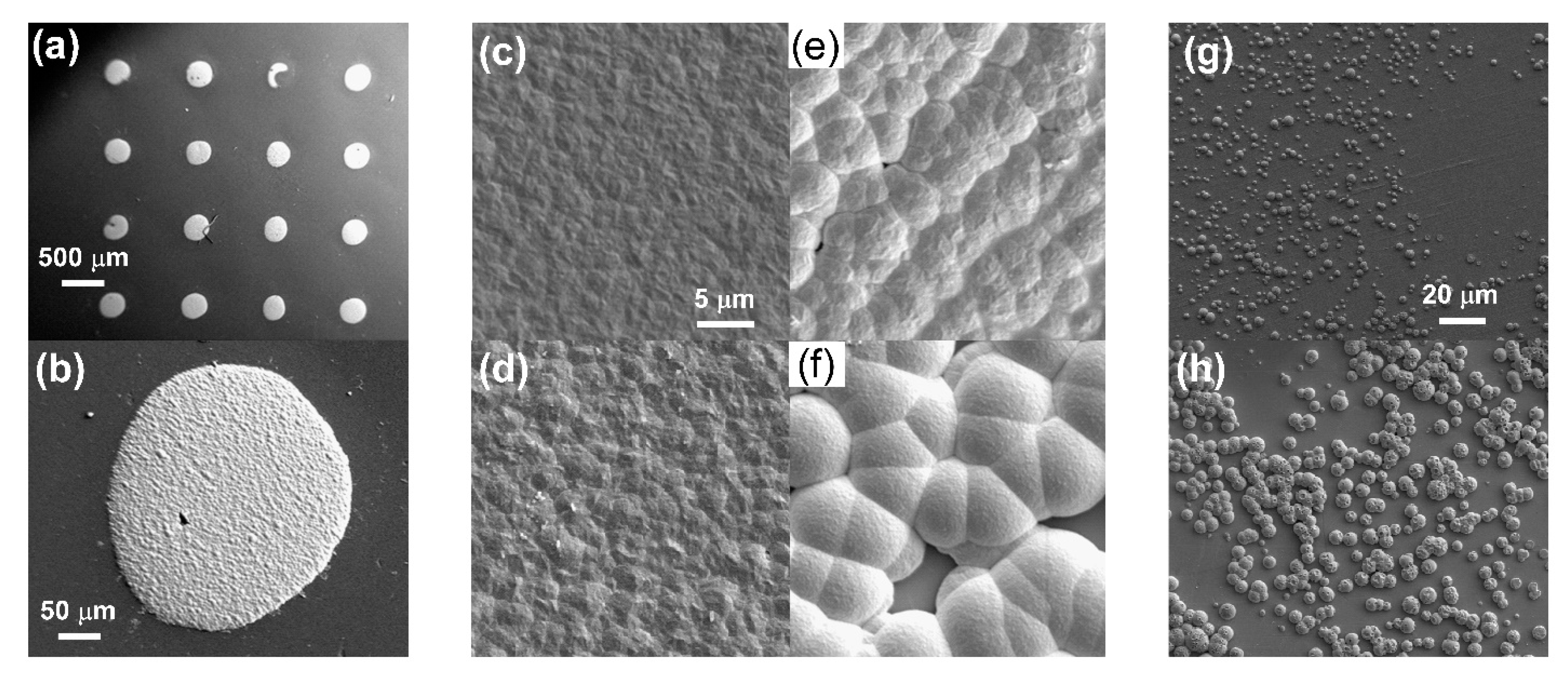
3.1. n-CLR Surface Structure Analysis

The structural features of n-CLR surfaces are characterized by pictures taken in secondary electron detection mode with a Zeiss™ EVO MA15 scanning electron microscope (SEM). SEM parameters of each picture shown in Figure 4 are detailed in Table 3.
Figure 4a shows a typical square 4 × 4 n-CLRs structure of 3.3 mm side, according to the ED mask pattern. The Figure 4b focuses to a single n-CLR exhibiting a circular continuous layer of about 300 µm in diameter, obtained by stopping ED when saturation current is reached (see Figure 2). A further magnification allows to detail the surface roughness of n-CLR surfaces made under various conditions. Figure 4c–e present for membrane A how surfaces change as a function of the ED voltage. The lowest cathodic voltage of −1.20 V induces a very smooth surface, with small crystalline structures (Figure 4c). Lowering the voltage down to 1.17 V allows to synthesize larger and sharper crystalline structures (Figure 4d). On the contrary, applying a larger voltage of −1.33 V induces rougher surfaces, made of a collection of small spheres joined together (Figure 4e). Finally, Figure 4f shows very large spheres joined together, made in a type B membrane at −1.25 V: typical of a low fluence membrane structure.
Figure 4 emphasizes that ED voltages and pore densities are adjustment parameters able to monitor the n-CLR surface textures. Other parameters like the NWs materials or pulsed ED modes, not studied yet, may also be used to tailor the surface structure of continuous layers.
In addition to continuous surface layers, granular surface structures can also be obtained by stopping the ED after the inflexion point but before reaching a continuous layer (Figure 2(b3)). This condition allows NW surface overgrowth under the shape of hemispherical grains, as presented in Figure 4g,h. The pore density sets the maximum size of the hemispheres: the lower the pore density, the more distant the pores from each other, the larger the hemispheres maximum size achievable. That is, the hemisphere diameter from about 300 nm to 30 µm for pore density ranging, respectively, from 1 × 109 cm−2 to 1 × 105 cm−2. Therefore, ED stopping time and pore density are the main adjustment parameters to tailor granular surface structures.

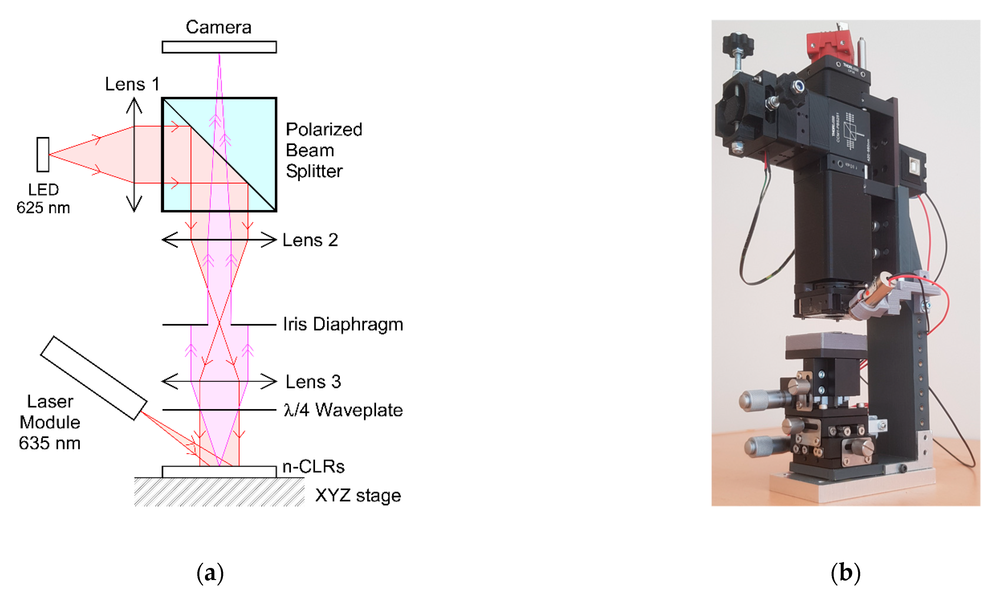
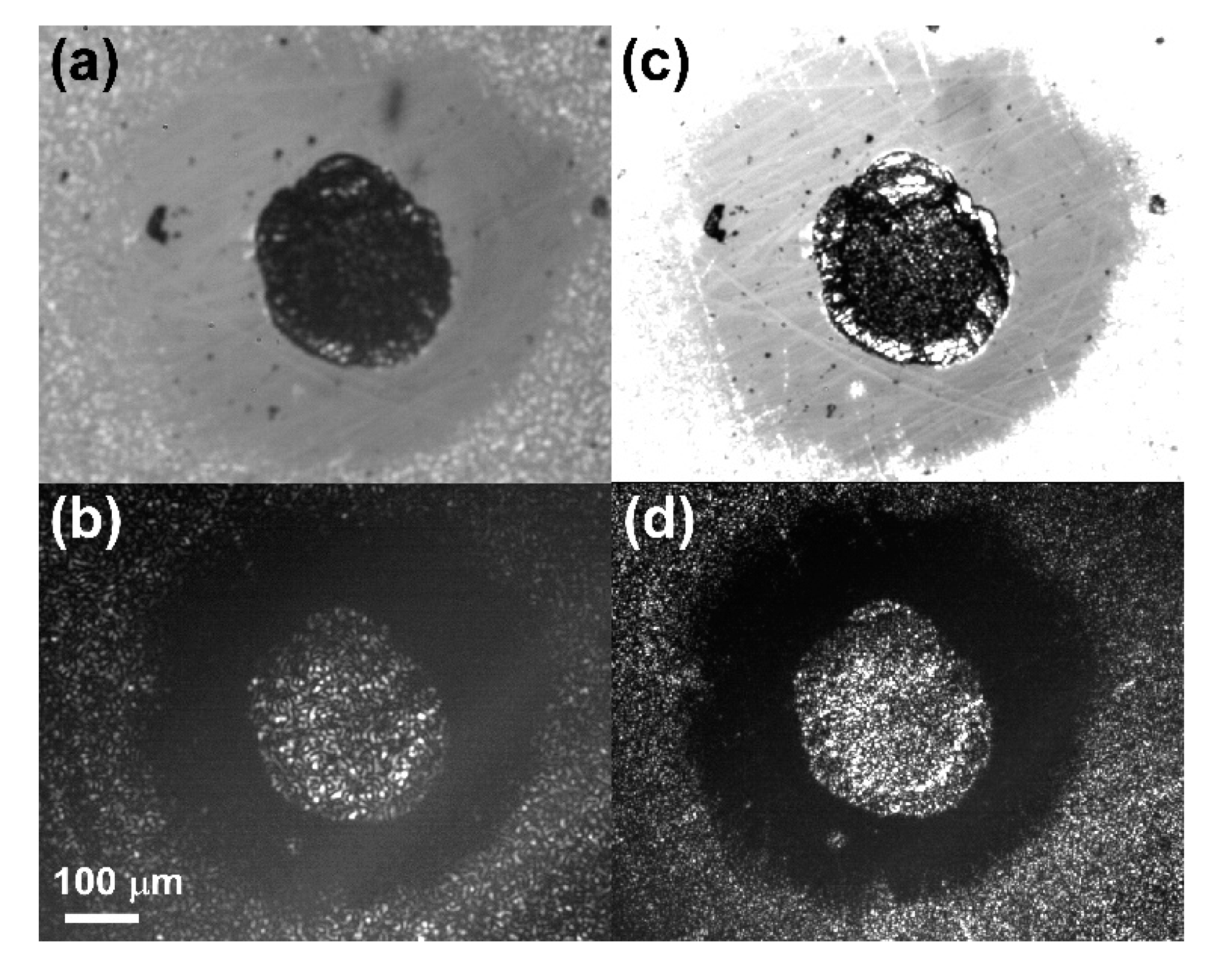
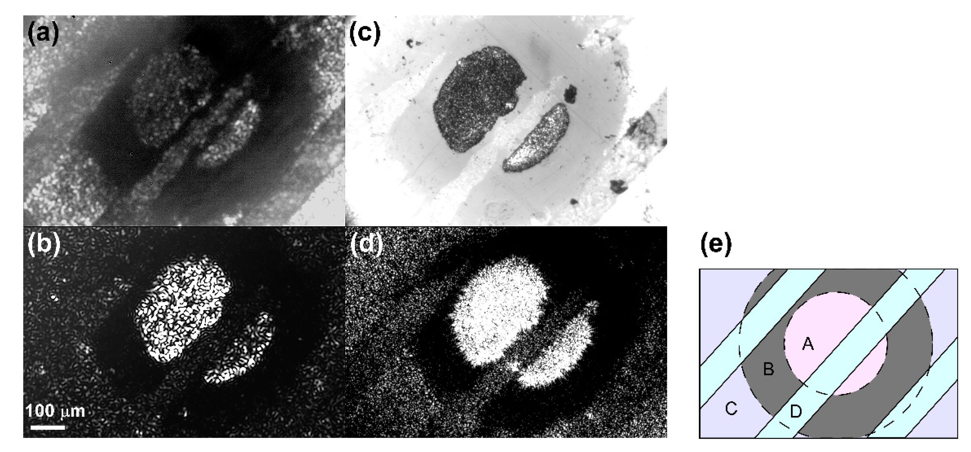
3.2. n-CLR Speckle Image Analysis

Figure 5 presents speckle images of an n-CLR, acquired with the optical setup in Figure 3. The LED light in confocal mode gives access to both real image of the sample and a speckle pattern. This lighting mode is very useful to analyze in the same image both the physical structure (shape, defects) and the speckle patterns of n-CLRs. However, the light reflection in the confocal mode strongly limits the contrast of the speckle pattern (Figure 5a,c). On the contrary, the laser light in the tilted incidence mode generates a high-contrast speckle pattern, but hides details on the n-CLR physical structure (Figure 5b,d).
The iris diaphragm diameter is an important adjustment parameter, which monitors the size and number of speckles captured by the camera: the closer the iris, the larger the speckles and the less their number, as shown for iris diaphragm diameters of 3.5 mm (Figure 5a,b) and 0.8 mm (Figure 5c,d).
Figure 5 exhibits three areas with distinct speckles patterns:
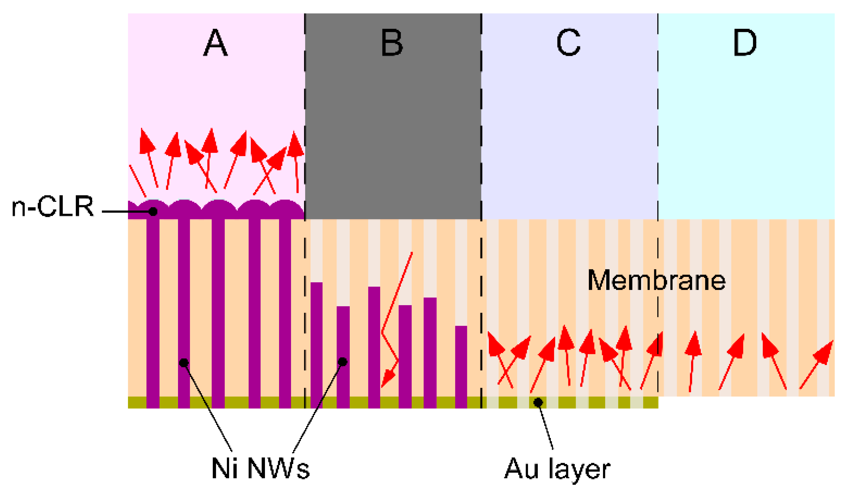
  • In the center, the n-CLR surface made by template synthesis. It appears quite dark in LED confocal illumination mode and exhibits speckles pattern. The direct laser illumination mode also exhibits speckles pattern, but brighter in contrast.
  • At the periphery of the image, the gold-coated membrane that also exhibits its own speckles pattern. It is overexposed in the LED confocal mode, since gold is more reflective than nickel, but less bright than the n-CLR in the laser illumination mode.
  • Between the two previous areas appears a “blind” area surrounding the n-CLR center, in which no speckle can be detected. This is the most interesting and unexpected feature of this work. In the in LED confocal illumination mode, the membrane top surface and its defects can then be seen in this area, which appears completely dark in the laser mode.
This “blind” area is attributed to the NWs embedded in the membrane around the n-CLR surface, due to partial ED at the edge of the NBR joint, as sketched in Figure 3. This array of vertically aligned NWs is a perfect photon trap which inhibits any light reflection. This phenomenon is reported in the literature for ultra-dark materials, as presented in [12]. This unexpected optical property sets a unique high-contrast feature in speckles images of NW-based n-CLRs.
Speckles images of granular n-CLRs are presented in Figure 6: in this case the poor contrast in the LED mode does not allow to detect the speckles but the real shape only (Figure 6a,c). On the contrary the laser mode is able to generate speckles in every grains (Figure 6b,d), providing the evidence that granular surface structures can be used for n-CLRs.

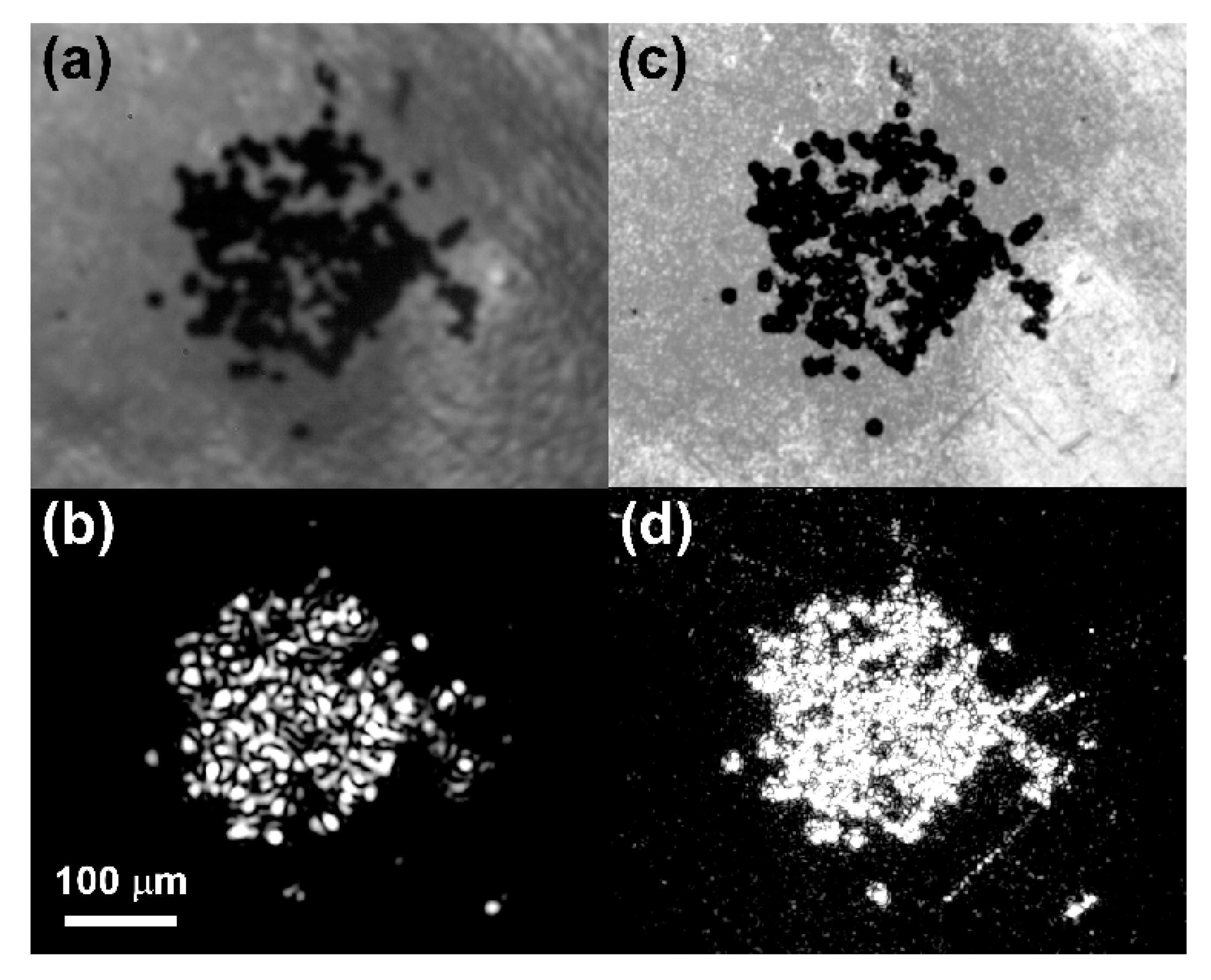
3.3. Full Patterned n-CLR Speckle Image

In order to explore the complete features of speckles images and the “blind” area, a specific n-CLR array was synthesized, by patterning under a PVD shadow mask the gold layer into 200 µm wide parallel stripes, with an interspace of 100 µm, as sketched in Figure 7e. The speckle images of such structures are presented in Figure 7a–d, in both LED and laser mode, which show four distinct speckle areas labeled in Figure 7e: (A) the n-CLR surfaces; (B) the “blind” area without speckles; (C) the gold-coated membrane and (D) the bare, uncoated membrane. Figure 8 draws the corresponding nanostructures of each area. This emphasizes the wide coding opportunities induced by crossing patterns of the gold layer and the ED mask.

4. Discussion

The numerous details shown by the speckle images in Figure 5, Figure 6 and Figure 7 propose n-CLRs as cost-effective flexible tags or barcodes, of which speckle images own numerous encoding parameters, as listed in Table 4. Most of these parameters range continuously, giving potentially an infinite number of coding levels. However, the number of levels is practically limited by the ability to distinguish the features in speckles patterns. It is also to note that this list can be furtherly enriched by any additional fabrication steps, such as membrane surface pre-treatment or any high-resolution lithographic methods.
To address this technology to large scale and low-cost production, further efforts are needed to make it completely mature, mainly in terms of (1) repeatability, (2) homogeneity, (3) surface recognition and (4) fast reading.
  • Repeatability: it is to achieve a finer control of the template synthesis NWs’ growth conditions in order to obtain the desired texture of n-CLRs in both continuous or granular surfaces. The foreseen techniques are at one hand by setting up sequenced or pulsed ED and at other hand by using other NWs’ materials, like Cu or Ni alloys.
  • Homogeneity: it is to insure equal growth conditions for each n-CLR in a single ED run. Here, current efforts are being made to switch from the actual all-purpose ED cell to a newly designed ED cell dedicated to n-CLR synthesis. The functional specifications of this new cell are of course to keep the fabrication steps number low, but also to mimic, as closely as possible, the current fabrication processes of PCB makers, to keep this technology open to cost-effective large-scale production.
  • Surface recognition: it is to bind a given random speckle pattern to a given surface texture. Ongoing works are in progress, which couple confocal microscopy images of n-CLR surfaces to speckles images numerical simulations, to be compared with real speckles images.
  • Fast reading: it is to identify a given n-CLR surface by its random speckle patterns as fast as possible [13,14]. Here, the goal is to identify the most relevant correlation parameters to be checked by existing images analysis algorithms [15]. To achieve this, a machine learning project is about to start, which aims to process the database of more than 1000 speckle images acquired during the present work. This work will address to the most effective numerical treatment of speckles images, and thus to fast n-CLR tags identification.

5. Conclusions

The present work demonstrates the feasibility of n-CLRs as low-cost nanostructured flexible tags for the tracking of large-scale fabrication products. n-CLRs fulfil the three rigorous criteria of marginal cost, simple identification and numerous adjustable parameters.
The fabrication process of n-CLRs is detailed, which combines one single lithography step of conventional metal coating to one single electrochemical step of template synthesis nanotechnology under ED masks, to produce self-organized micro- and/or nanostructured surfaces. This process uses closely PCB industry techniques, to achieve low-cost, large series productions. Nevertheless, further efforts are needed to improve the ED step in terms of repeatability and homogeneity.
A simple, fast and cheap optical reading technique is presented, that lights up n-CLRs with LED or laser beams and captures speckles diffraction images. Works are currently in progress to set a formal identification of n-CLR surfaces via their random speckle patterns. In a next step, speckle features have to be analyzed by machine learning to define a set of relevant correlation parameters, able to ensure a very fast and secure identification of n-CLRs by conventional image processing algorithms.
The adjustable fabrication parameters are listed and analyzed in terms of speckle image features. They are not only quite numerous, but also offer a wide range of levels each. The precise number of levels will depend on the fineness of the random speckle pattern analysis achievable by machine leaning. Nevertheless, n-CLRs propose a set of parameters fair enough to ensure a large coding range.
The most surprising feature is the “blind” area in which speckles are completely inhibited. This is attributed to the ultra-dark effect of arrays of vertically aligned NWs embedded into the membrane, that trap and absorb incoming photons. This unexpected phenomenon proposes a very unique, high-contrast optical parameter only achievable in n-CLR thin film structures. Future works will aim at patterning this “blind” area.

Author Contributions

Conceptualization, L.G. and Y.S.; methodology, L.G., D.P. and J.M.; validation, L.G.; investigation, D.P., J.M. and M.L.; data curation, D.P. and M.L.; writing—original draft preparation, L.G. and Y.S.; writing—review and editing, L.G.; visualization, L.G.; supervision, L.G. and Y.S.; project administration, L.G.; funding acquisition, L.G. and Y.S. All authors have read and agreed to the published version of the manuscript.

Funding

This research was funded by HES-SO//University of Applied Sciences and Arts Western Switzerland, grant number 90546.

Data Availability Statement

Data supporting reported results have not yet been deposited in a publicly available database. This will be done during review. Accession numbers will be provided prior to publication.

Acknowledgments

Authors gratefully acknowledge Pierre Burdet for the SEM pictures.

Conflicts of Interest

The authors declare no conflict of interest.

References

  1. Ren, W.; Lin, G.; Clarke, C.; Zhou, J.; Jin, D. Optical Nanomaterials and Enabling Technologies for High-Security-Level Anticounterfeiting. Adv. Mater. 2019, 32, e1901430. [Google Scholar] [CrossRef] [PubMed]
  2. Smith, A.F.; Skrabalak, S.E. Metal nanomaterials for optical anti-counterfeit labels. J. Mater. Chem. C 2017, 5, 3207–3215. [Google Scholar] [CrossRef]
  3. Blau, Y.; Bar-On, O.; Hanein, Y.; Boag, A.; Scheuer, J. Meta-hologram-based authentication scheme employing a speckle pattern fingerprint. Opt. Express 2020, 28, 8924–8936. [Google Scholar] [CrossRef] [PubMed]
  4. Tomescu, R.; Parvulescu, C.; Cristea, D.; Comanescu, B.; Pelteacu, M. Low cost technology for the fabrication of anti-counterfeiting microtaggants. J. Micromech. Microeng. 2021, 31, 035008. [Google Scholar] [CrossRef]
  5. Pérez-Mitta, G.; Toimil-Molares, M.E.; Trautmann, C.; Marmisollé, W.A.; Azzaroni, O. Molecular Design of Solid-State Nanopores: Fundamental Concepts and Applications. Adv. Mater. 2019, 31, e1901483. [Google Scholar] [CrossRef] [PubMed]
  6. Enculescu, I.; Siwy, Z.; Dobrev, D.; Trautmann, C.; Molares, M.T.; Neumann, R.; Hjort, K.; Westerberg, L.; Spohr, R. Copper nanowires electrodeposited in etched single-ion track templates. Appl. Phys. A 2003, 77, 751–755. [Google Scholar] [CrossRef]
  7. it4ip. Available online: www.it4ip.be (accessed on 31 July 2021).
  8. Lindeberg, M.; Hjort, K. A comprehensive study of ion track enabled high aspect ratio microstructures in flexible circuit boards. Microsyst. Technol. 2004, 10, 608–621. [Google Scholar] [CrossRef]
  9. Péter, L. Electrochemical Methods of Nanostructure Preparation; Springer: Cham, Switzerland, 2021. [Google Scholar] [CrossRef]
  10. Matei, E.; Enculescu, I.; Toimil-Molares, M.E.; Leca, A.; Ghica, C.; Kuncser, V. Magnetic configurations of Ni–Cu alloy nanowires obtained by the template method. J. Nanoparticle Res. 2013, 15, 1863. [Google Scholar] [CrossRef]
  11. Lindeberg, M.; Yousef, H.; Rödjegård, H.; Martin, H.; Hjort, K. A PCB-like process for vertically configured thermopiles. J. Micromech. Microeng. 2008, 18, 065021. [Google Scholar] [CrossRef] [Green Version]
  12. Jackson, J.J.; Puretzky, A.A.; More, K.L.; Rouleau, C.M.; Eres, G.; Geohegan, D.B.; Puretzky, A. Pulsed Growth of Vertically Aligned Nanotube Arrays with Variable Density. ACS Nano 2010, 4, 7573–7581. [Google Scholar] [CrossRef] [PubMed]
  13. Carnicer, A.; Javidi, B. Optical security and authentication using nanoscale and thin-film structures. Adv. Opt. Photonics 2017, 9, 218–256. [Google Scholar] [CrossRef] [Green Version]
  14. Mwema, F.M.; Akinlabi, E.T.; Oladijo, O.P.; Fatoba, O.S.; Akinlabi, S.A.; Tălu, S. Advances in manufacturing analysis: Fractal theory in modern manufacturing. In Modern Manufacturing Processes; Woodhead Publishing: Sawston, UK, 2020; pp. 13–39. [Google Scholar] [CrossRef]
  15. Gonzalez, R.C.; Woods, R.E.; Eddins, S.L. Digital Image Processing Using Matlab, 3rd ed.; Gatesmark Publishing: Knoxville, TN, USA, 2020. [Google Scholar]
Figure 1. Presentation of the ED cell: (a) descriptive scheme of its working principle; (b) picture of the ED cell, the overall height of the mechanical structure is about 17 cm.
Applnano 02 00023 g001
Figure 2. (a) Chronoamperometric curves both performed at V E D = 1.25 V. Full orange line: membrane A (high pore density). Dotted blue line: membrane B (low por density). The cathodic reduction current is presented here as negative. The slightly larger thickness of the curves at final saturation is due to oscillations in the growth rate induces by the flow pulses of the peristaltic pump. (b) Schematic cross-sectional view of the membrane during template synthesis. Pore diameters are here strongly exaggerated for the sake of clarity. (1) Before ED; (2) NWs growth; (3) inflexion point; (4) saturation. Residual NWs growth occurs at the fringe of the NBR joint.
Applnano 02 00023 g002
Figure 3. (a) Working principle of the optical setup for speckle images acquisition. Red beams indicate lights shining the n-CLR, the pink beam indicates the light emitted by the n-CLR surface and captured by the camera. Either the LED or the laser module are used as light source. All optical components are fixed, except the distance between the n-CLR and the lens 3 which can be adjusted to focus the image on the camera. (b) Picture of the optical setup. Its overall height is about 30 cm.
Applnano 02 00023 g003
Figure 4. SEM pictures of the n-CLR surfaces. (a) View of a 4 × 4 n-CLR sample just after electrodeposition; (b) zoom in on a single n-CLR, about 300 µm in diameter; (cf) details of n-CLR continuous surfaces with various textures, depending on the growth conditions; (c) membrane A, V E D = 1.20 V; (d) membrane A, V E D = 1.17 V; (e) membrane C, V E D = 1.33 V; (f) membrane D, V E D = 1.25 V; (g) granular n-CLR surface, membrane A, V E D = 1.90 V; (h) granular n-CLR surface, membrane B, V E D = 1.25 V.
Applnano 02 00023 g004
Figure 5. Representative speckle images of one n-CLR (Membrane A, V E D = 1.20 V). Light source: LED (a,c) and laser (b,d). Iris diphragm opening: 0.8 mm (a,b) and 3.5 mm (c,d).
Applnano 02 00023 g005
Figure 6. (a) Speckle images of a granular n-CLR (Membrane B, V E D = 1.25 V). Light source: LED (a,c) and laser (b,d). Iris diphragm opening: 0.8 mm (a,b) and 3.5 mm (c,d).
Applnano 02 00023 g006
Figure 7. Speckle images of one patterned n-CLR (Membrane A, V E D = 1.20 V). The gold layer is patterned in parallel stripes. Light source: LED (a,c) and laser (b,d). Iris diphragm opening: 0.8 mm (a,b) and 3.5 mm (c,d). (e) Scheme of the pattern. Area A: ED with overgrown NWs. Aera B: NWs embedded into the membrane. Area C: membrane with gold layer but without NWs. Area D: bare membrane without gold layer nor NWs.
Applnano 02 00023 g007
Figure 8. Schematic cross-section view of a patterned n-CLR. Pore diameters are here strongly exaggerated for the sake of clarity. Arrows indicates the reflexion of the incoming light giving speckle interferences, except for the area B, where the arrow skectches the multi-reflection process that traps photons. (A) ED with overgrown NWs; (B) NWs embedded into the membrane; (C) membrane with gold layer but without NWs; (D) bare membrane without gold layer nor NWs.
Applnano 02 00023 g008
Table 1. Parameters of the track-etched membranes used in this work.
MembranePore DensityPore DiameterThicknessPolymer
A 1 × 10 9 cm−250 nm25 µmPI
B 4 × 10 8 cm−2
Table 2. Part list of the optical setup.
PartProviderReference
Lens 1Thorlabs™AC080-010-A-ML
Lens 2Thorlabs™AC254-080-A-ML
Lens 3Thorlabs™AC080-016-A-ML
Polarized Beam SplitterThorlabs™CCM1-PBS251
Iris DiaphragmThorlabs™CP20S
Quarter Wave-PlateThorlabs™WPQ10M-633
LEDOSRAM™LR G6SP
Laser ModuleThorlabs™PL202
CameraAllied Vision™AV ALVIUM 1800U-500M-CH-C
Table 3. SEM parameters of pictures in Figure 4.
PictureMagnificationAcceleration Voltage [kV]Working Distance [mm]
4a5010.008.12
4b50010.008.07
4c50005.006.29
4d50005.005.48
4e50005.005.31
4f50005.005.58
4g10005.005.39
4h10005.005.62
Table 4. Adjustable physical parameters of n-CLRs, and their corresponding speckle image features available for encoding.
Physical Control ParameterSpeckle Image Features
Membrane polymerBare membrane speckles
Pore densityGranular surface speckles
Metal coating patternMetal coating speckles
ED mask patternn-CLRs surfaces speckles
ED mask pattern“Blind” dark speckleless area
Material for NWs EDn-CLR surface reflectivity
ED voltagen-CLR surface texture, roughness
ED duration timeGranular to continuous n-CLR surfaces
Iris diaphragm apertureSpeckle size and number
Publisher’s Note: MDPI stays neutral with regard to jurisdictional claims in published maps and institutional affiliations.

