Abstract
The rational synthesis of semiconducting materials with enhanced photoelectrocatalytic efficiency under visible light illumination is a long-standing issue. ZnO has been systematically explored in this field, as it offers the feasibility to grow a wide range of nanocrystal morphology; however, its wide band gap precludes visible light absorption. We report on a novel method for the controlled growth of semiconductor heterostructures and, in particular, core/sheath ZnO/MoS2 nanowire arrays and the evaluation of their photoelectrochemical efficiency in oxygen evolution reaction. ZnO nanowire arrays, with a narrow distribution of nanowire diameters, were grown on FTO substrates by chemical bath deposition. Layers of Mo metal at various thicknesses were sputtered on the nanowire surface, and the Mo layers were sulfurized at low temperature, providing in a controlled way few layers of MoS2, in the range from one to three monolayers. The heterostructures were characterized by electron microscopy (SEM, TEM) and spectroscopy (XPS, Raman, PL). The photoelectrochemical properties of the heterostructures were found to depend on the thickness of the pre-deposited Mo film, exhibiting maximum efficiency for moderate values of Mo film thickness. Long-term stability, in relation to similar heterostructures in the literature, has been observed.
1. Introduction
The quick depletion of natural resources and moderation of carbon dioxide emissions are currently pursued by developing low-cost alternatives of electricity supply using renewable energy sources, such as solar light. Photoelectrochemical (PEC) water splitting stands out as a promising way towards hydrogen production by solar energy-driven water splitting. Metal oxide semiconductors, such as TiO2 [1,2,3], ZnO [4,5,6] and WO3 [7,8], have traditionally been employed as anodes in PEC cells in view of their stability and ease of morphology manipulation, especially for ZnO [9,10]. However, the wide optical bandgaps of these materials limit their light absorption only to the UV part of the solar spectrum, which prevents the efficient exploitation of solar energy in the visible region. Hematite (α-Fe2O3), an abundant and non-toxic material, has also been intensively explored owing to its narrow bandgap (~2.1 eV) for solar water splitting [11], which is, however, bound to several limitations, such as low absorption, short exciton lifetime and low oxygen evolution reaction kinetics. An additional narrow bandgap semiconductor, i.e., BiVO4, has also been systematically investigated for potential use as a photoanode in solar water splitting, despite it suffers from very low electron-hole separation yield, leading to poor efficiency conversion [12].
Recently, hybrid core/sheath nanostructures consisting of a metal oxide semiconductor core (ZnO) covered by transition metal di-chalcogenides layers (MX2, M: Mo, W, etc., and X: Se, S2, Te) and other chalcogenides, such as ZnSe [13,14], CdS [15] and CdSe [16,17], have been explored as potential efficient PEC anode materials stimulated by visible light benefiting from a more effective separation of photo-generated charges.
Among various layered (2D) chalcogenide crystals, MoS2 is considered a promising material because of its tunable bandgap ranging from ~1.2 eV (indirect gap) for the bulk crystal to ~1.9 eV (direct gap) for the monolayer [18,19,20]. MoS2 comprises a strong in-plane covalent bonding of S–Mo–S and weak out-of-plane van der Waals interaction between S–S in neighboring layers, further exhibiting relatively high mobility [21]. According to theoretical calculations and experimental studies, MoS2 has high catalytic performance due to the S atoms situated at the edges of the plane, being more catalytically active than the S atoms of the basal sites of the layer [22,23,24] MoS2 can be synthesized by several methods, including hydrothermal [25], chemical vapor deposition [26], mechanical or chemical exfoliation [27], liquid-phase exfoliation [28], atomic layer deposition [29], and so on. Furthermore, MoS2 exhibits a variety of morphologies such as nanoparticles [30], nanotubes [31], nanosheets [32], flakes [33] and quantum dots [28,34].
There are few sporadic studies about the electrochemical behavior of MoS2 towards hydrogen evolution reaction (HER) [35]. However, the performance of the material in relation to the oxygen evolution reaction (OER) has not yet been explored systematically. Contrary to HER, the OER involves a four-electrons-step oxidation process and suffers from sluggish electrode kinetics [36]. In line with experiments and theoretical calculations, the defected edge sites and vacancies in the MoS2 can also promote the OER [34].
In this work, we attempt to investigate the OER of core/sheath ZnO/MoS2 heterostructures synthesized by a novel route. ZnO nanowire (NW) arrays prepared on FTO/glass substrates by chemical bath deposition stand as the scaffolds onto which the few-layer MoS2 thin films are grown. MoS2 sheath is prepared by low-temperature sulfurization of pre-deposited ultrathin Mo films on the ZnO surface. Controlling Mo film deposition and sulfurization conditions, heterostructures with varying thickness of MoS2 layers down to the monolayer, are prepared. Structural and morphological characterization is employed to provide information on microstructural characteristics of the heterostructures and the chemical environment of the interface between the core and sheath materials. The influence of the thickness of the sheath layer on the PEC properties of these hybrid nanostructures is explored.
2. Experimental
2.1. Growth of ZnO NW Arrays on FTO Substrates
The synthesis of ZnO NW arrays onto FTO/glass substrates has been described in detail elsewhere [37]. After the standard cleaning of the substrates, the method includes the dissolution of 0.05 M of zinc acetate dihydrate, ZnAc (Zn(CH3COO)2 ∙ 2H2O, Sigma-Aldrich ACS reagent, ≥98%) in absolute ethanol. The solution is spin-coated on the substrate and thermally decomposed to form the oriented nanocrystals of the ZnO seed layer. Subsequently, the growth of ZnO NW arrays takes place in an aqueous solution containing equimolar concentrations (0.035 M) of ZnAc and hexamethylenetetramine (HMTA, C6H12N4, Sigma-Aldrich, Louis, MI, USA, ACS reagent, ≥99.0%). The growth proceeds in a closed reactor vessel at 95 °C for 5 h. After the growth step, the NW arrays are rinsed with triple distilled water and annealed at 300 °C for 2 h.
2.2. Growth of ZnO/MoS2 Heterostructures
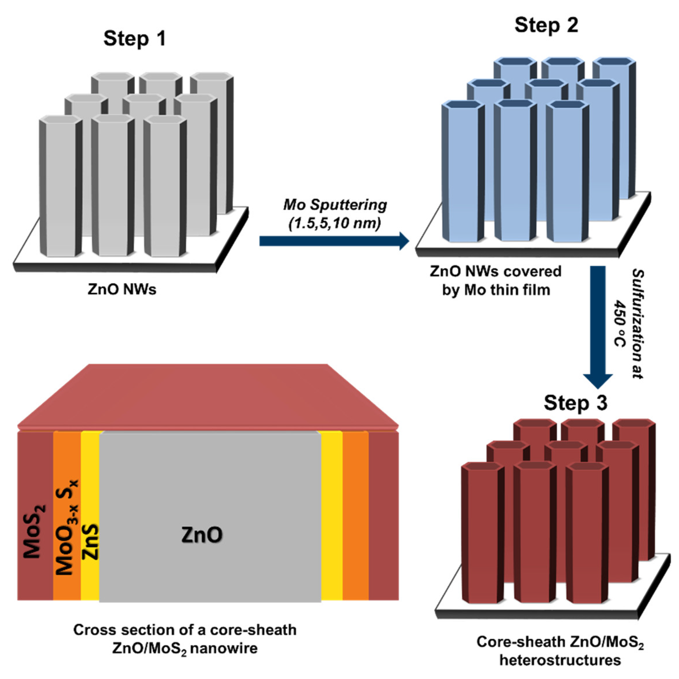
Mo ultrathin films of various nominal thicknesses ranging from 1.5 to 10 nm were deposited on the ZnO surface using sputtering at low vacuum (5 × 10⁻² mbar). For the formation of the MoS2 layer, the Mo-sputtered ZnO samples were placed into a triple temperature zone furnace to sulfurize the Mo films by exposing them to sulfur vapors. Specifically, sulfur powder (Alfa Aesar, 99.9999%) was placed in an alumina boat and positioned upstream in the quartz tube of the tube furnace, while the Mo-sputtered ZnO samples were placed downstream, a few cm away from the sulfur powder. The temperature was set at 450 °C for the Mo-covered ZnO NW arrays, while sulfur powder was heated at ~150–200 °C. Prior to increasing the temperature, Ar gas was purged into the reactor with a flow rate of 100 sccm for at least 60 min to remove the residual oxygen. The purging was kept during the heating phase, so Ar played the role of the carrier gas for the sulfur species in the gaseous phase. The nominal thickness of the sputtered Mo ultrathin film was found to control the number of MoS2 monolayers. After the heating phase (60 min), the furnace was allowed to cool down naturally until room temperature while being continuously purged by Ar gas. Scheme 1 provides a pictorial illustration of the various synthesis steps and a cross-section of the layers that comprise the final product. The MoS2/ZnO heterostructures prepared by pre-depositing 1.5, 5 and 10 nm of Mo metal are labeled hereafter as Mo-1.5, Mo-5 and Mo-10, respectively.
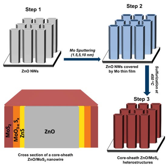
Scheme 1.
A schematic of the total synthesis procedure and an overview of the cross-section of the final product.
2.3. Characterization of Morphology, Structure and Optical Properties
The morphology of the ZnO/MoS2 heterostructures was characterized using field emission scanning electron microscopy (FE-SEM, Zeiss SUPRA, 35VP-FEG) operating at 15 keV and transmission electron microscopy (TEM, JEOL JEM-2100) operating at 200 kV. The crystal structure was verified by selected area electron diffraction (SAED). ZnO/MoS2 NWs were dispersed in alcohol and spread onto a carbon-coated copper grid (200 mesh) for the TEM analysis. The chemical composition of heterostructures and their interface were characterized with X-ray photoelectron spectroscopy (XPS) and X-ray induced Auger electron spectroscopy (XAES) in an ultrahigh vacuum chamber equipped with a SPECS Phoibos 100-1D-DLD hemispherical electron analyzer and a dual Al/Mg x-ray gun. The XP spectra were recorded with MgKa at 1253.6 eV photon energy and an analyzer pass energy of 10 eV, giving a full width at half maximum (FWHM) of 0.85 eV for the Ag3d5/2 line. The samples were mounted on a stainless-steel sample holder to avoid charging effects. The C1s position was at 285.0 eV due to carbon contamination. The crystallinity and thickness of the few-layer MoS2 were investigated via Raman spectroscopy (Jobin-Yvon, LabRam HR-800) using the excitation of 441.6 nm. A microscope objective with 50× magnification is used to focus the light onto a spot of about 3 μm in diameter. The optical properties were characterized by photoluminescence (PL) spectroscopy (Cary Eclipse Fluorescence Spectrophotometer G9800A, Agilent Technologies, Burlington, VT, USA, excitation at 500 nm) and ultraviolet-visible (UV-Vis) spectroscopy (Hitachi, U-3000).
2.4. Photoelectrochemical Measurements
The geometric area of the PEC anodes is about 2 × 2 cm2, while the electrode working area illuminated and exposed to the electrolyte was ~1 cm2. PEC characterization was performed using a three-electrode configuration and an AUTOLAB potentiostat (PGSTAT30 model). A Pt wire and a hydrogen reference electrode were used as counter and reference electrodes, respectively. The electrolyte was an aqueous solution of 0.24 M Na2S 9H2O (Sigma-Aldrich ACS reagent ≥ 98%) and 0.35 M Na2SO3 (Sigma-Aldrich ≥ 98%), pH 11.5, which was degassed by bubbling pure Ar for at least 30 min prior to the electrical measurements to remove dissolved gases. The light source (solar simulator) comprised a 150 W Xe arc lamp delivering an intensity of 100 mW cm−2. The sample was illuminated from the backside (bare glass surface). The electrochemical characterization and the evaluation of the heterostructures were observed by performing linear sweep voltammetry (LSV) and cyclic voltammetry (CV) with a scan rate of 50 mV s−1.
3. Results and Discussion
3.1. Electron Microscopy Analysis
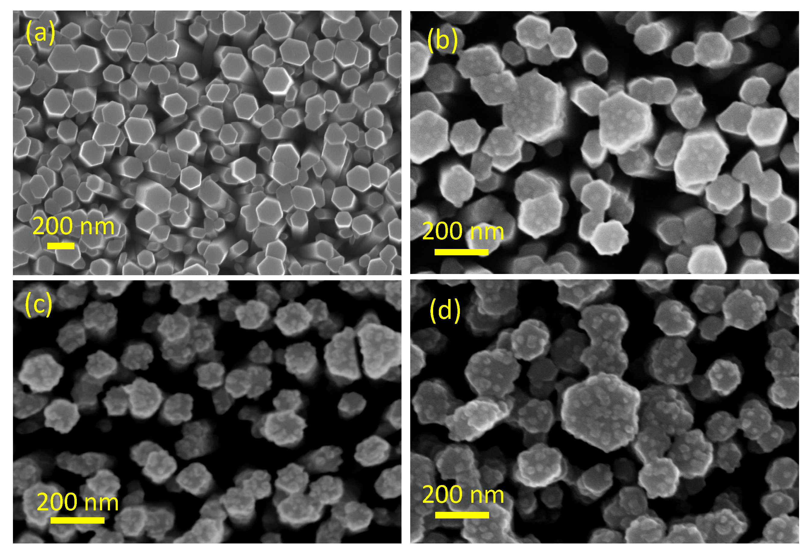
Figure 1 displays the FE-SEM images of the (a) bare ZnO NRs and (b–d) the heterostructures with a different layer thickness of MoS2 sheath; (b), (c), and (d) correspond to Μο-1.5, Μο-5 and Μο-10, respectively. The 1D rod-like ZnO structures are clearly observed in all cases. The average diameter of ZnO NWs is approximately 120 nm, while their length is ~1 μm. FE-SEM images reveal that the initially smooth surface of the ZnO NWs (a) attain a textured form due to the growth of the MoS2 sheath. The effect becomes progressively more evident as the nominal Mo thickness increases from 1.5 to 10 nm. The formation of the sheath is apparent for all thicknesses of pre-deposited Mo films. In the case of Mo-5 nm and Mo-10, FE-SEM reveals the growth of islands, especially on the top of the rods.
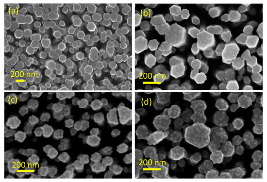
Figure 1.
SEM images of (a) bare ZnO NWs. (b–d) denote ZnO/MoS2 heterostructures with Mo nominal thickness of 1.5, 5 and 10 nm, respectively.
The morphology and the core/sheath structure of the nanorods are further investigated by TEM and high-resolution TEM (HRTEM). Figure 2a,b show low-magnification TEM micrographs of ZnO NWs and the Mo-10 ZnO/MoS2 heterostructure. The MoS2 sheath is evidenced by the semitransparent film grown around the ZnO nanowire in Figure 2b. The HRTEM image in Figure 2c illustrates the interplanar distances of (002) ZnO planes, with the corresponding lattice spacing at 0.26 nm. Additionally, Figure 2d displays the interlayer arrangement of hexagonal 2H-MoS2 with a lattice spacing of approximately 0.62 nm, corresponding to the spacing d(002) of hexagonal 2H-MoS2. In the same area, we can spot the d(100) of MoS2 estimated as ~0.27 nm.
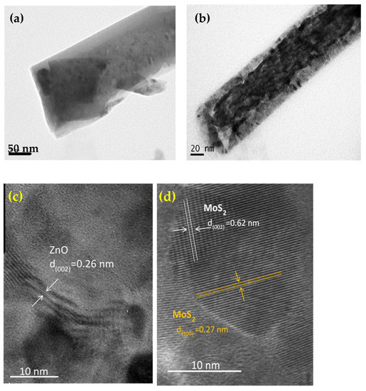
Figure 2.
TEM images (a) a ZnO NW and (b) a ZnO/MoS2 core/sheath heterostructure. HRTEM of (c) ZnO and (d) hexagonal MoS2 showing the crystal planes (002) and (100).
3.2. XPS Analysis
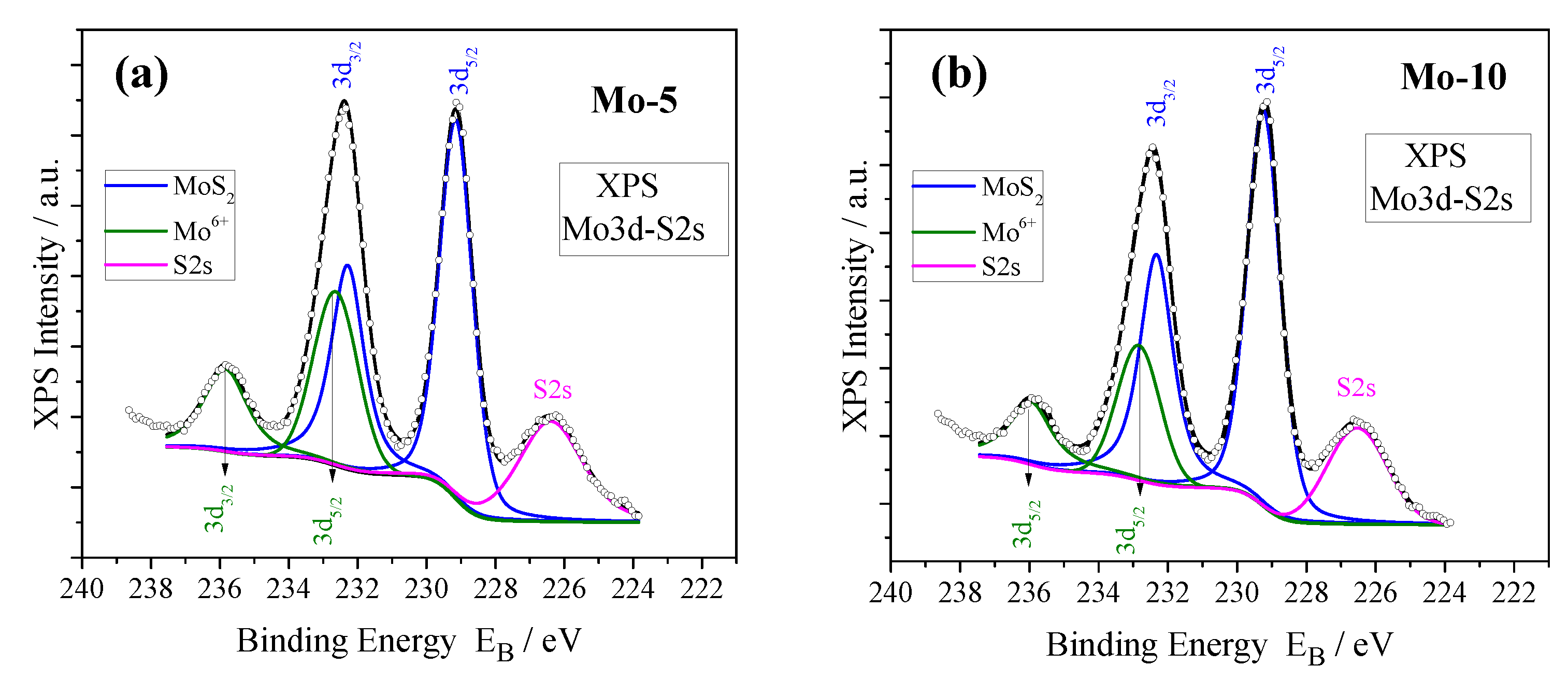
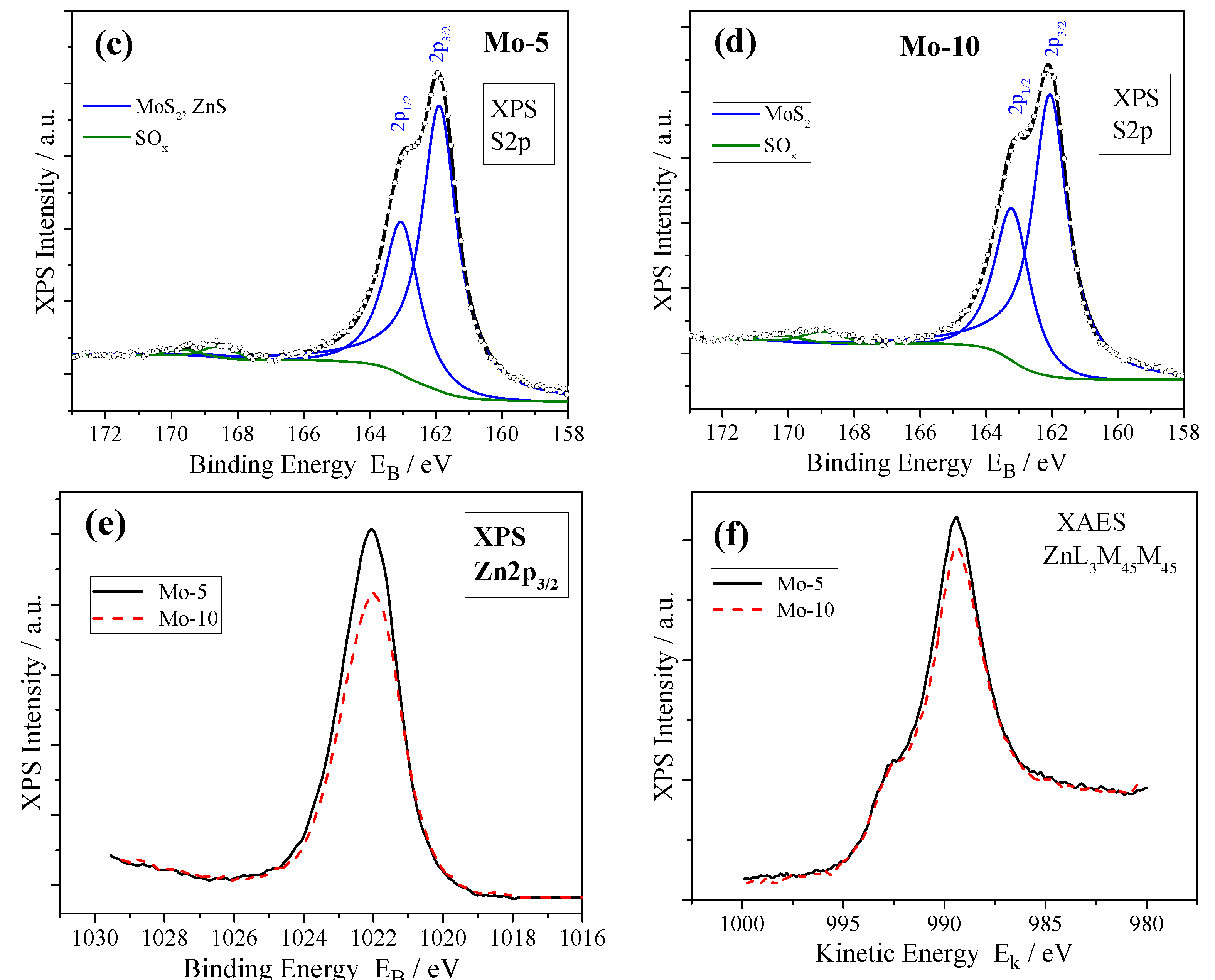
XPS survey scans, shown in Figure S1, for the heterostructures show that Zn, Mo, S, C and O elements are present. The XPS spectra of the combined Mo3d-S2s window are shown in Figure 3a,b. The Mo3d peak is analyzed into two Mo3d doublets with the spin-orbit splitting of 3.2 eV and with binding energies (BE) of Mo3d5/2 peak at 229.2 eV assigned to 2H-MoS2 [38] and at 232.5 eV assigned to Mo+6 chemical state of a mixed oxysulfide MoO3-xSx species [39]. The % concentration of the MoS2 component is ~65% and ~72% for Mo-5 and Mo-10 heterostructures, respectively. Figure 3c,d show the S2p XPS peaks, which consist of S2p doublets with the spin-orbit splitting of 1.2 eV. The BE of the S2p3/2 peak is found at 161.9 eV and can be assigned to species related to MoS2 and ZnS since the S2p3/2 peak for both components lies at nearly the same BE [38,40]. Traces of sulfur oxide are revealed by the weak peak at 168.9 eV assigned to sulphates (SO4 anions) and/or sulphite (SO3 anions) species [41] Figure 3e,f display the Zn2p3/2 spectra and the ZnLMM X-ray-induced Auger spectra, respectively. Since the literature values for the Zn 2p3/2 BEs are quite similar for ZnS and ZnO, the Auger parameter, defined as the sum of the binding energy of the Zn 2p3/2 and the kinetic energy of the Zn M3L45L45, is an accurate parameter for the chemical state identification. The obtained value 2011.5 eV is in agreement with that reported in the literature for zinc(II) sulfide [40].
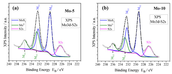
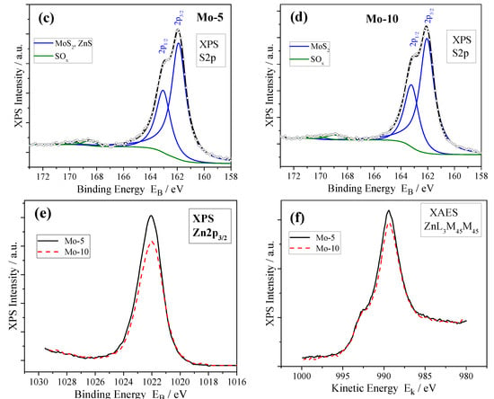
Figure 3.
(a,b) Deconvoluted Mo3d XPS peak of Mo-5 and Mo-10 heterostructures. (c,d) Deconvoluted S2p XPS peak of Mo-5 and Mo-10 heterostructures. (e,f) Zn2p3/2 spectra and ZnLMM XAES spectra of Mo-5 and Mo-10 heterostructures.
The relative atomic concentration of Mo, S and Zn have been derived using the Mo3d, S2p and Zn2p3/2 peak areas, weighted by the relative sensitivity factors and the transmission characteristics of the energy analyzer. The atomic mass ratios for the M-5 and Mo-10 heterostructures are estimated as Mo/S/Zn = 20.0/57.9/22.1 and Mo/S/Zn = 18.4/63.7/17.9, respectively. These ratios declare that the Mo/S ratio is considerably lower than the nominal value, 1/2. This finding is not unexcepted given that sulfurization not only proceeds towards complete reaction with the Mo thin film, but it further takes place at a deeper level, transforming the topmost atomic layers of ZnO to ZnS and/or ZnOyS1-y. Therefore, the chemical species information furnished by XPS indicates the lack of an abrupt interface between MoS2 and ZnO. Instead, there is a thin zone of gradual transformation between these two materials, with this zone being composed of oxy-sulfide species and possibly mixed MoO3-xSx and ZnOyS1-y species. While an abrupt interface between the two semiconductors may impose a barrier, which must be overcome by photogenerated charge carriers, the gradual variation originating from these mixed species may offer more favorable conditions for efficient charge transport and separation.
3.3. Optical Properties
3.3.1. PL Spectroscopy
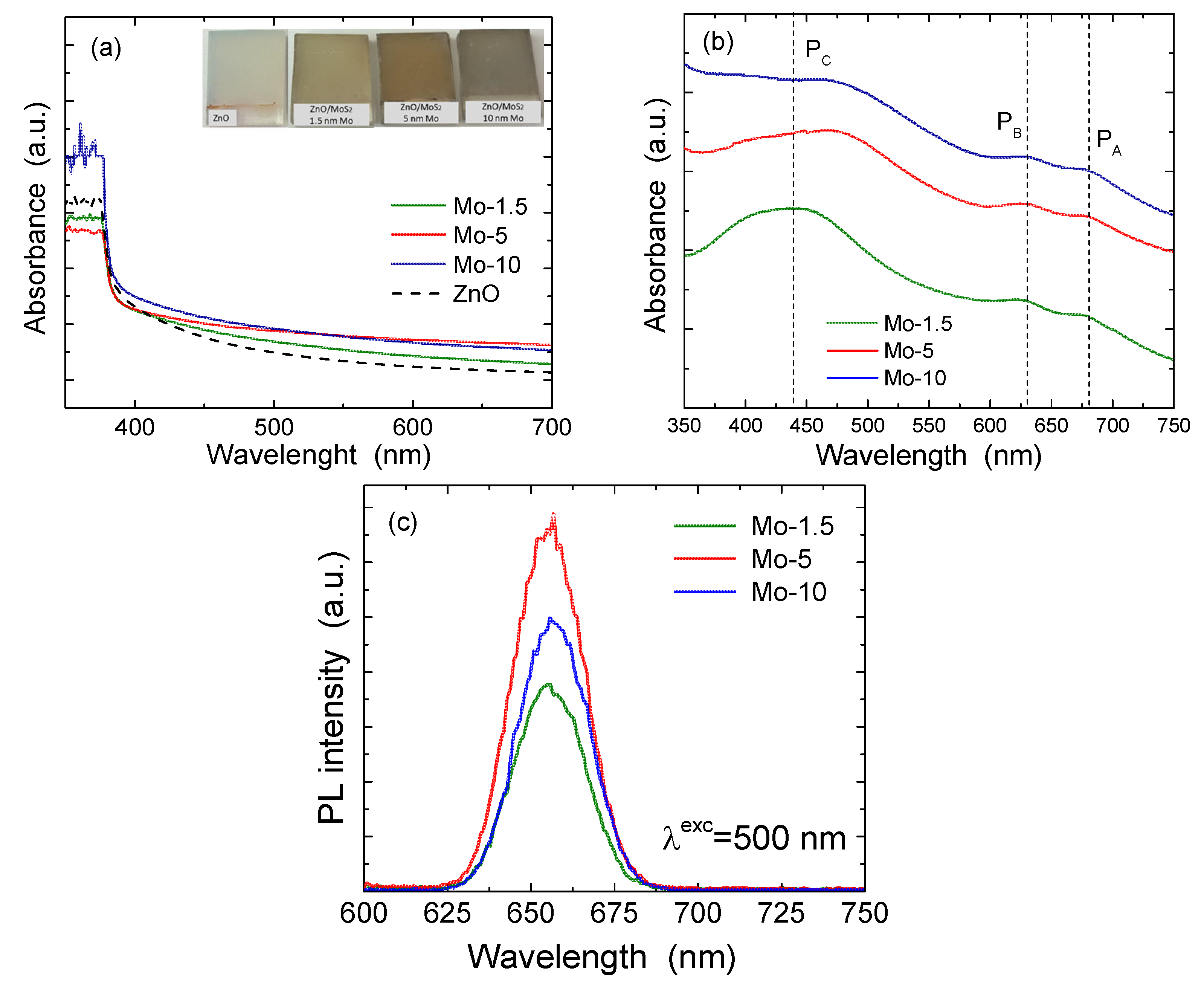
Optical properties of the ZnO/MoS2 heterostructures were investigated using UV-Vis absorption and PL spectroscopies. Figure 4a shows the UV-Vis absorption spectra of the bare ZnO nanorod array (dashed line) and the ZnO/MoS2 heterostructures. The color change from light to dark colored when the Mo film thickness increases is visible in the optical images shown in the inset. This causes a slight increase in the absorption curves at the visible wavelengths. Because the thickness of the MoS2 shell around ZnO is very low (few monolayers), only the absorption of ZnO in the UV region (~380 nm) becomes dominant. To observe the fine details of absorption peaks of MoS2 in the visible region, MoS2 films were grown on bare FTO glass substrates by sulfurizing pre-deposited Mo thin films with the same nominal thicknesses, i.e., 1.5, 5 and 10 nm. These MoS2 samples on a bare FTO exhibit two peaks (PA and PB) at 675 and 625 nm, as shown in Figure 4b. These two excitonic peaks correspond to the “A” and “B” transitions between the split maxima of the valence band and the conduction band minimum at the K point of the Brillouin zone [18]. The band near 440 nm, for the sample grown using 1.5 nm of Mo, corresponds to the transition “C” assigned to the van Hove singularities in the electronic density of states [42].
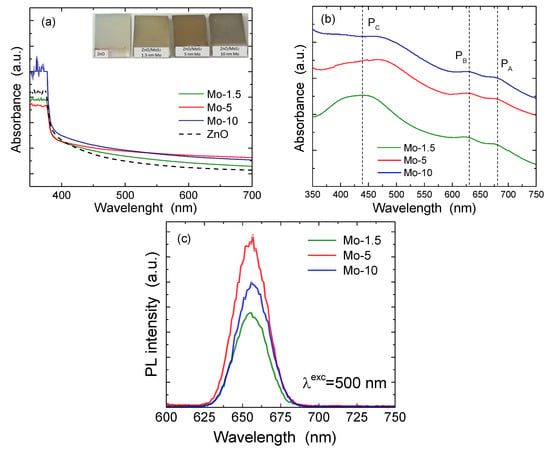
Figure 4.
(a) UV-vis absorption spectra of the bare ZnO and ZnO/MoS2 heterostructures; the inset shows optical images of the samples. (b) Absorption spectra of MoS2 films deposited on FTO glass substrate. (c) Photoluminescence spectra of ZnO/MoS2 heterostructures (excitation at 500 nm).
The PL spectra, shown in Figure 4c, were recorded with excitation energy of 500 nm. Since a conventional PL instrument was used, the PL signal arises from a very wide area of about a few mm2, hence being representative of the sample homogeneity. For all three heterostructures, the spectra consist of one emission peak at around 655 nm, which is attributed to the direct band gap transitions at the K point of the Brillouin zone. The position of the PL peaks is almost unchanged for the three different heterostructures. In addition, the PL intensity does not substantially increase with decreasing MoS2 thickness, down to the monolayer. There are two main factors that the current data cannot be directly compared to the literature data. First, as mentioned above, the PL spectra have been acquired in a way that the spot on the sample surface is several mm2 averaging a vast number of sites, while most PL data in the literature pertains to micro-PL measurements using laser beam focusing by objectives. Second, the electronic structure of MoS2 layers grown on ZnO using the current method differs considerably from that of neat MoS2 films because the ZnO-MoS2 interface introduces mixed metal oxo-sulfide species, as evidenced by the XPS analysis. Such mixed species are expected to alter the PL properties of neat MoS2.
3.3.2. Raman Spectroscopy
Raman spectroscopy was employed to study crystallinity and estimate the thickness of the MoS2 films on ZnO NWs. Representative Raman spectra are shown in Figure 5a, confirming the growth of 2H-MoS2. A representative full-range Raman spectrum is shown in Figure S2. In all cases, the Raman spectra exhibit two intense bands at ~385 and ~407 cm−1, corresponding to the out-of-plane and in-plane modes, respectively. The first mode results from vibrations of S atoms in opposite directions, while the second mode is associated with the opposite vibration of two S atoms with respect to the Mo atom [19]. Based on the proposed correlation [16,18] between the number of MoS2 monolayers and the peak frequency difference (Δω) between and modes, the thickness of the MoS2 sheath was estimated, and it is illustrated in Figure 5b. The solid squares in Figure 5b denote the points of the correlation proposed in [18]. The data of the current work revealed that the difference in Δω (= − ) increases from 19.5 to 21.6 when the Mo-sputtered film increases from 1.5 to 10 nm. These values correspond to layer thickness of MoS2 of roughly 1, 2 and (less than) 3 monolayers for the Mo films of 1.5, 5 and 10 nm, respectively. This finding dictates that the preparation method employed in this work can offer to tune the thickness of the MoS2 sheath layer with monolayer resolution. This is important considering that the optical bandgap energy of MoS2 strongly depends on the number of layers at the few monolayers limit.
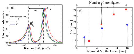
Figure 5.
(a) Raman spectra of ZnO/MoS2 heterostructures. (b) The dependence of Δω vs. the nominal Mo thickness (solid spheres). The solid squares denote the dependence of Δω against the number of MoS2 monolayers taken from Ref. [18].
4. Photoelectrochemical Measurements
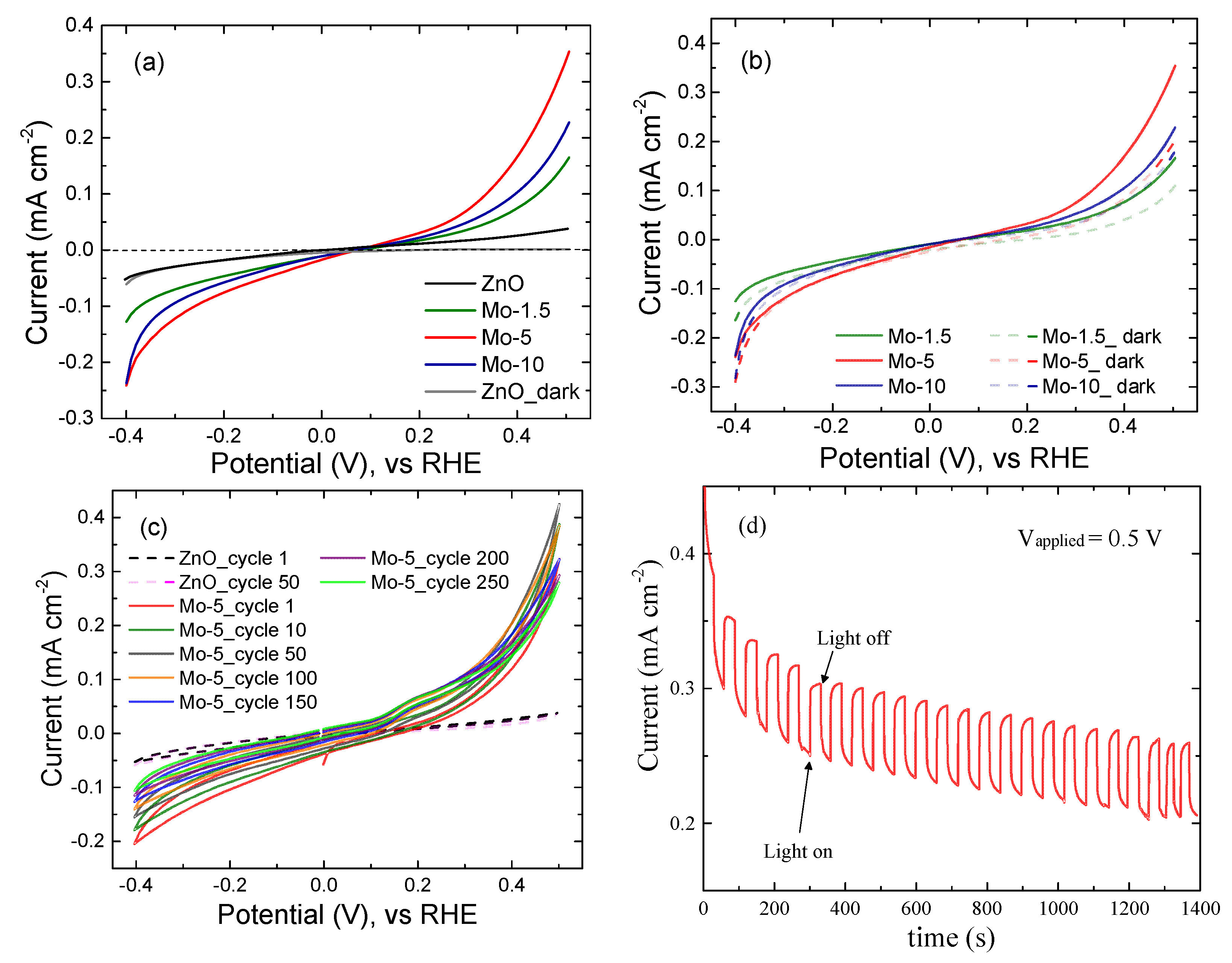
To evaluate the PEC activity of the heterostructures, linear sweep voltammetry curves (LSV) were performed both in the dark (dashed lines) and under illumination (solid lines) conditions. LSV curves of bare ZnO and ZnO/MoS2 heterostructures with a different nominal thickness of Mo are presented in Figure 6a. It is observed that the onset potential of bare ZnO under illumination is comparable with that of the ZnO/MoS2 structure (Figure 6a). The onset potential for all the ZnO/MoS2 heterostructures is approximately the same and around 0.15 V vs. RHE. Other studies such as Jian et al. [31] observed an obvious cathodic shift of the onset potential for the ZnO/MoS2 nanocables morphology in comparison with bare ZnO.
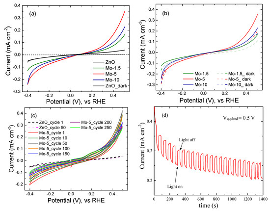
Figure 6.
(a,b) LSV curves both in the dark and under illumination of bare ZnO and ZnO/MoS2 heterostructures with different nominal Mo thicknesses (scan rate 50 mV s−1). (c) Cyclic voltammetry curves of bare ZnO NWs and ZnO/MoS2 heterostructures for the Mo-5 sample. (d) Chronoamperometric curve (J vs. t) for the Mo-5 sample at the applied potential of 0.5 V vs. RHE under chopped illumination.
The photocurrent density is improved for all the ZnO/MoS2 samples and does not seem to reach the saturation current value up to 0.5 V vs. RHE. The data reveal a non-monotonic dependence of the current vs. the pre-deposited Mo film thickness. In particular, the Mo-5 heterostructures are found to exhibit the best activity towards OER with a photocurrent value equal to 0.35 mA cm−2 at 0.5 V, which is almost 10 times higher than that of bare ZnO NWs. Further increase in the MoS2 thickness causes a decrease in the photocurrent density of about 34 % in relation to the maximum value. The layer-dependent electrocatalysis can be correlated to the hopping of electrons in the vertical direction of MoS2 layers over an interlayer potential barrier, according to Cao et al. [43], who observed that the catalytic activity of MoS2 deteriorates by a factor of ~4.5 for every additional layer of MoS2. On the other hand, Trung et al. [33] prepared ZnO/MoS2 heterostructures with two different thicknesses of Mo, 90 nm and 140 nm, to observe the catalytic dependence from the thickness of MoS2 layers. They concluded that the thicker sheath of MoS2 was catalytically more active; however, only by a few %. The non-monotonic dependence of the current density observed in the current investigation calls for a rational explanation, as it is not a trivial finding in relevant studies. Although the reason underlying this effect is still debatable, this non-monotonic behavior could potentially be accounted for in the following context. The change in the photoanode performance (i.e., current density) depends upon two competing factors. One is related to the increase in the thickness (coverage) of the MoS2 sheath, which causes an increase in the absorbed visible photons. The latter stimulate charge carrier generation and hence enhanced water splitting. On the other hand, the increase in the deposited Mo metal film indicates that a wider interfacial zone among the two semiconductors is being built up. The latter and the possible presence of traces of unreacted Mo metal at the interfacial zone could be an inhibiting factor for efficient charge separation. The two aforementioned competing factors seem to compromise each other, providing the best performance at the moderate MoS2 thickness, i.e., the Mo-5 sample.
The value of the ZnO dark current is significantly lower than the photocurrent. As shown in Figure 6a with black and grey lines, respectively. However, in the case of ZnO/MoS2 heterostructures, the dark current has a measurable value, as depicted in Figure 6b. The dark current indicates that chemical reactions can take place in the interface between the photoanode and the electrolyte in the absence of illumination. In this context, the ZnO/MoS2 heterostructures also exhibit electrocatalytic behavior. Except for electrocatalysis, the dark current may attribute to electro-corrosion of MoS2, in which active S atoms can react with redox species in the solution [31].
The stability of the bare ZnO and ZnO/MoS2 heterostructure with the best catalytic performance (Mo-5 sample) has further been examined by cyclic voltammetry (CV) measurements, as illustrated in Figure 6c. The CV curves are carried out in the range of −0.4 V to 0.5 V vs. RHE under illumination. The anode of the bare ZnO NWs is stable after 50 cycles. The ZnO/MoS2 sample shows an improved behavior after 10 cycles, while at the 50th cycle, it has its maximum photocurrent value of 0.42 mA cm−2 at 0.5 V vs. RHE. After the 50th cycle, the photocurrent starts to deteriorate until it reaches the initial value after 150 cycles.
Figure 6d displays the photocurrent response of the Mo-5 sample for several on–off cycles at an applied potential of 0.5 V vs. RHE under chopped illumination. When illumination commences, a sharp increase in the current response is increased, which is attributed to the photogeneration of charged carriers. The current response in the dark does not approach the zero values, indicating that ZnO/MoS2 heterostructures also exhibit electrocatalytic behavior in accordance with their high values of dark currents, shown in Figure 6b.
The photocurrent of the Mo-5 sample exhibits presents reliable stability up to 1400 s, presumably due to the sacrificial polysulfide electrolyte as Na2S acts as a hole scavenger. As it has already been reported elsewhere [44,45], this type of electrolyte diminishes photocorrosion of the catalyst’s surface, while aqueous electrolytes, such as KOH or Na2SO4, lead to surface dissolution. It is worth mentioning that the stability in the current study extends to much longer periods than those reported in previous PEC investigations, i.e., 600 s in [31] and 500 s in [33].
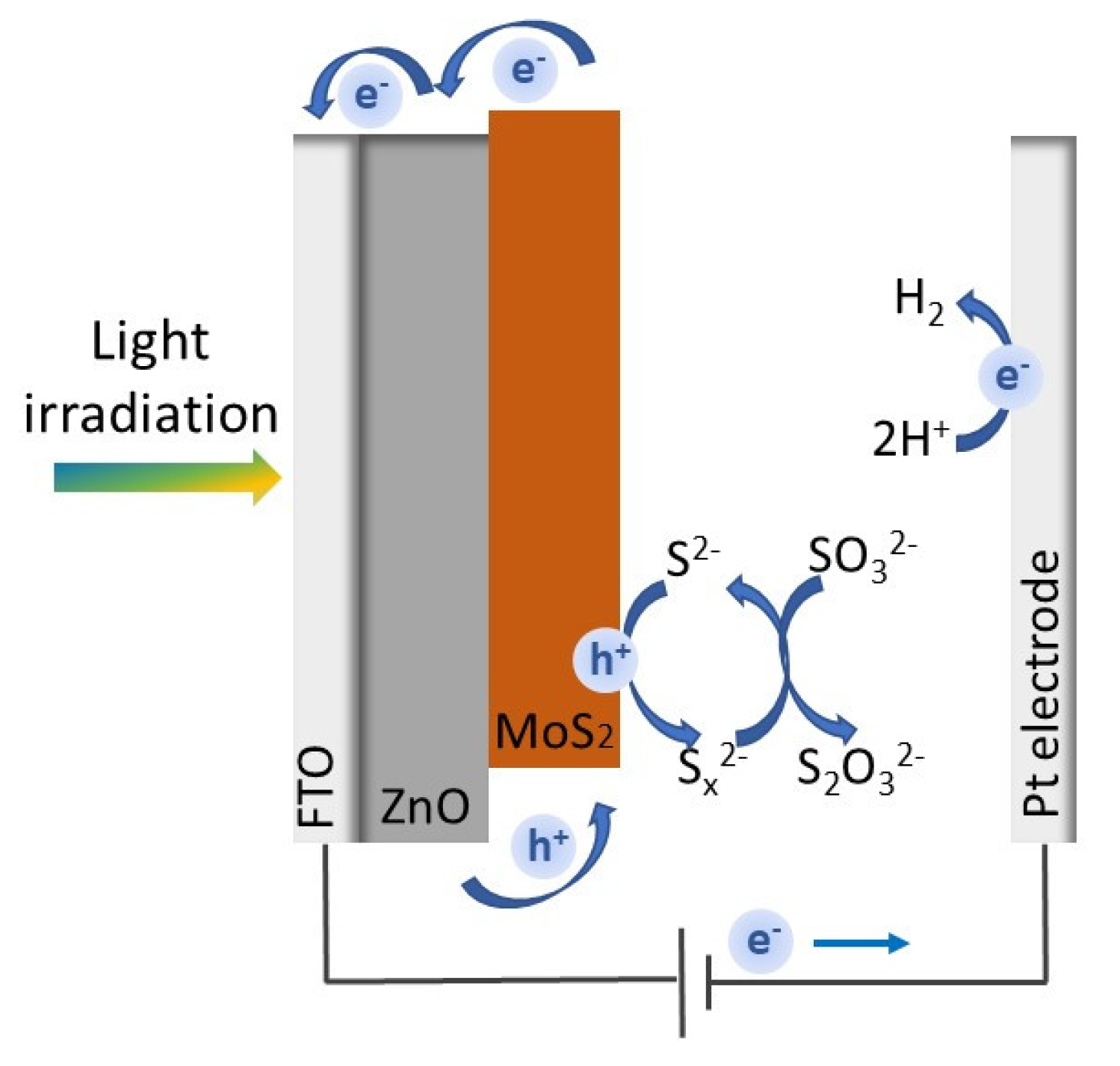
The ZnO/MoS2 heterostructure is essentially a p-n junction where energy band alignment takes place at the interface. The reactions describing the water-splitting process in the current case are depicted by the reactions (1) to (4). The absorption of photons with energy close or higher than the optical bandgap causes the creation of electron–holes pairs (reaction 1). The electrons transport through the ZnO NWs to the FTO substrate and then are transferred through the external circuit to the Pt counter electrode to induce hydrogen production. The holes travel to the semiconductor/ electrolyte interface and react with ions from the electrolyte molecules to form (reaction 2). The ions from Na2SO3 reduce to (reaction 3), and they can react with to generate (reaction 4) to prevent sulfur deposition.
Figure 7 illustrates the separation and transport processes of the photoinduced charge carriers in the photoelectrochemical water splitting process over the ZnO/MoS2 heterostructure.
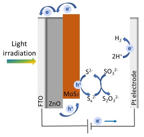
Figure 7.
A schematic of the charge carriers’ reactions in a PEC splitting cell.
5. Conclusions
In summary, well-aligned ZnO/MoS2 core/sheath heterostructures have been grown on FTO/glass substrate by a sequence of synthesis methods, comprising chemical bath deposition of the ZnO nanowire arrays and Mo sputtering followed by low-temperature sulfurization. The current approach offers control over the final thickness of the MoS2 layer grown on ZnO. Electron microscopy and spectroscopic techniques have provided information on the morphology, thickness and details of the interface between the two semiconductors, i.e., ZnO and MoS2. It has been found that the Mo thin films thickness, which is pre-deposited on ZnO NWs surface, determines the MoS2 thickness under particular growth (sulfurization) conditions. XPS measurements have revealed a variety of chemical species beyond the ZnO and MoS2. In particular, the current work provides evidence about a non-abrupt interface between the two semiconductors. The composition of the interface changes gradually from the core towards the shell in the following sequence ZnO → ZnOyS1-y and/or ZnS → MoO3-xSx → MoS2. PEC measurements have shown a clear improvement of the photocurrent for all heterostructures in comparison to the neat ZnO NW arrays and a very good long-term stability. The heterostructures prepared with sulfurization of Mo film with a nominal thickness of ca. 5 nm have shown the best photocurrent and enhanced stability.
Supplementary Materials
The following are available online at https://www.mdpi.com/article/10.3390/applnano2030012/s1, Figure S1: XPS survey scans, Figure S2: Raman spectrum.
Author Contributions
Conceptualization, S.N.Y. and S.G.N.; methodology, K.G., A.A. and L.S.; investigation, K.G., A.A. and L.S.; writing—original draft preparation, K.G., A.A., L.S., S.G.N. and S.N.Y.; writing—review and editing, K.G. and S.N.Y.; supervision, S.N.Y. and S.G.N.; funding acquisition, S.N.Y. and S.G.N.; All authors have read and agreed to the published version of the manuscript.
Funding
This research is co-financed by Greece and the European Union (European Social Fund- ESF) through the Operational Programme “Human Resources Development, Education and Lifelong Learning 2014–2020” in the context of the project Photo-electrochemical water splitting with combination of 1-D and 2-D structures” (MIS 5047755).
Institutional Review Board Statement
Not applicable.
Informed Consent Statement
Not applicable.
Data Availability Statement
Not applicable.
Acknowledgments
The authors wish to thank FORTH/ICE-HT for providing experimental facilities and Mary Kollia (Laboratory of Electron Microscopy and Microanalysis, School of Natural Sciences, University of Patras) for the TEM images.
Conflicts of Interest
The authors declare no conflict of interest.
References
- Ni, M.; Leung, M.K.H.; Leung, D.Y.C.; Sumathy, K. A review and recent developments in photocatalytic water-splitting using TiO2 for hydrogen production. Renew. Sustain. Energy Rev. 2007, 11, 401–425. [Google Scholar] [CrossRef]
- Nowotny, J.; Bak, T.; Nowotny, M.K.; Sheppard, L.R. Titanium dioxide for solar-hydrogen I. Functional properties. Int. J. Hydrogen Energy 2007, 32, 2609–2629. [Google Scholar] [CrossRef]
- Fujishima, A.; Zhang, X.; Tryk, D.A. TiO2 photocatalysis and related surface phenomena. Surf. Sci. Rep. 2008, 63, 515–582. [Google Scholar] [CrossRef]
- Wolcott, A.; Smith, W.A.; Kuykendall, T.R.; Zhao, Y.; Zhang, J.Z. Photoelectrochemical Study of Nanostructured ZnO Thin Films for Hydrogen Generation from Water Splitting. Adv. Funct. Mater. 2009, 19, 1849–1856. [Google Scholar] [CrossRef]
- Shet, S. Zinc Oxide (ZnO) Nanostructures for Photoelectrochemical Water Splitting Application. ECS Trans. 2007, 33, 15–25. [Google Scholar] [CrossRef]
- Nguyen, D.-T.; Shin, E.-C.; Cho, D.-C.; Chae, K.-W.; Lee, J.-S. Photoelectrochemical performance of ZnO thin film anodes prepared by solution method. Int. J. Hydrogen Energy 2014, 39, 20764–20770. [Google Scholar] [CrossRef]
- Santato, C.; Ulmann, M.; Augustynski, J. Enhanced Visible Light Conversion Efficiency Using Nanocrystalline WO3 Films. Adv. Mater. 2001, 13, 511–514. [Google Scholar] [CrossRef]
- Seabold, J.A.; Choi, K.S. Effect of a cobalt-based oxygen evolution catalyst on the stability and the selectivity of photo-oxidation reactions of a WO3 photoanode. Chem. Mater. 2011, 23, 1105–1112. [Google Scholar] [CrossRef]
- Wang, Z.L. ZnO nanowire and nanobelt platform for nanotechnology. Mater. Sci. Eng. R Rep. 2009, 64, 33–71. [Google Scholar] [CrossRef]
- Wang, Z.L. Zinc oxide nanostructures: Growth, properties and applications. J. Phys. Condens. Matter 2004, 16, R829–R858. [Google Scholar] [CrossRef]
- Tamirat, A.G.; Rick, J.; Dubale, A.A.; Su, W.-N.; Hwang, B.-J. Using hematite for photoelectrochemical water splitting: A review of current progress and challenges. Nanoscale Horiz. 2016, 1, 243–267. [Google Scholar] [CrossRef]
- Kim, T.W.; Choi, K.-S. Nanoporous BiVO4 Photoanodes with Dual-Layer Oxygen Evolution Catalysts for Solar Water Splitting. Science 2014, 343, 990–994. [Google Scholar] [CrossRef]
- Wang, L.; Tian, G.; Chen, Y.; Xiao, Y.; Fu, H. In situ formation of a ZnO/ZnSe nanonail array as a photoelectrode for enhanced photoelectrochemical water oxidation performance. Nanoscale 2016. [Google Scholar] [CrossRef] [PubMed]
- Cho, S.; Jang, J.-W.; Lim, S.-H.; Kang, H.J.; Rhee, S.-W.; Lee, J.S.; Lee, K.-H. Solution-based fabrication of ZnO/ZnSe heterostructure nanowire arrays for solar energy conversion. J. Mater. Chem. 2011, 21, 17816. [Google Scholar] [CrossRef] [Green Version]
- Xu, H.; Mo, R.; Cheng, C.; Ai, G.; Chen, Q.; Yang, S.; Li, H.; Zhong, J. ZnSe/CdS/CdSe triple-sensitized ZnO nanowire arrays for multi-bandgap photoelectrochemical hydrogen generation. RSC Adv. 2014, 4, 47429–47435. [Google Scholar] [CrossRef]
- Ouyang, W.X.; Yu, Y.X.; Zhang, W. De High and stable photoelectrochemical activity of ZnO/ZnSe/CdSe/CuxS core-shell nanowire arrays: Nanoporous surface with CuxS as a hole mediator. Phys. Chem. Chem. Phys. 2015, 17, 14827–14835. [Google Scholar] [CrossRef]
- Chen, Y.; Wang, L.; Wang, W.; Cao, M. Enhanced photoelectrochemical properties of ZnO/ZnSe/CdSe/Cu2-xSe core–shell nanowire arrays fabricated by ion-replacement method. Appl. Catal. B Environ. 2017, 209, 110–117. [Google Scholar] [CrossRef]
- Lee, C.; Yan, H.; Brus, L.E.; Heinz, T.F.; Hone, Ќ.J.; Ryu, S. Anomalous Lattice Vibrations of Single and Few-Layer MoS2. ACS Nano 2010, 4, 2695–2700. [Google Scholar] [CrossRef] [Green Version]
- Li, H.; Zhang, Q.; Yap, C.C.R.; Tay, B.K.; Edwin, T.H.T.; Olivier, A.; Baillargeat, D. From Bulk to Monolayer MoS2: Evolution of Raman Scattering. Adv. Funct. Mater. 2012, 22, 1385–1390. [Google Scholar] [CrossRef]
- Mak, K.F.; Lee, C.; Hone, J.; Shan, J.; Heinz, T.F. Atomically thin MoS2: A new direct-gap semiconductor. Phys. Rev. Lett. 2010, 105, 2–5. [Google Scholar] [CrossRef] [PubMed] [Green Version]
- Kang, K.; Xie, S.; Huang, L.; Han, Y.; Huang, P.Y.; Mak, K.F.; Kim, C.-J.; Muller, D.; Park, J. High-mobility three-atom-thick semiconducting films with wafer-scale homogeneity. Nature 2015, 520, 656–660. [Google Scholar] [CrossRef] [PubMed]
- Salmeron, M.; Somorjai, G.A.; Wold, A.; Chianelli, R.; Liang, K.S. The adsorption and binding of thiophene, butene and H2S on the basal plane of MoS2 single crystals. Chem. Phys. Lett. 1982, 90, 105–107. [Google Scholar] [CrossRef]
- Helveg, S.; Lauritsen, J.V.; Lægsgaard, E.; Stensgaard, I.; Nørskov, J.K.; Clausen, B.S.; Topsøe, H.; Besenbacher, F. Atomic-Scale Structure of Single-Layer MoS2 Nanoclusters. Phys. Rev. Lett. 2000, 84, 951–954. [Google Scholar] [CrossRef] [Green Version]
- Jaramillo, T.F.; Jorgensen, K.P.; Bonde, J.; Nielsen, J.H.; Horch, S.; Chorkendorff, I. Identification of Active Edge Sites for Electrochemical H2 Evolution from MoS2 Nanocatalysts. Science 2007, 317, 100–102. [Google Scholar] [CrossRef] [PubMed] [Green Version]
- Yuan, Y.-J.; Wang, F.; Hu, B.; Lu, H.-W.; Yu, Z.-T.; Zou, Z.-G. Significant enhancement in photocatalytic hydrogen evolution from water using a MoS2 nanosheet-coated ZnO heterostructure photocatalyst. Dalton Trans. 2015, 44, 10997–11003. [Google Scholar] [CrossRef]
- Lee, Y.H.; Zhang, X.Q.; Zhang, W.; Chang, M.T.; Lin, C.T.; Di Chang, K.; Yu, Y.C.; Wang, J.T.W.; Chang, C.S.; Li, L.J.; et al. Synthesis of large-area MoS2 atomic layers with chemical vapor deposition. Adv. Mater. 2012, 24, 2320–2325. [Google Scholar] [CrossRef] [Green Version]
- Chhowalla, M.; Shin, H.S.; Eda, G.; Li, L.-J.; Loh, K.P.; Zhang, H. The chemistry of two-dimensional layered transition metal dichalcogenide nanosheets. Nat. Chem. 2013, 5, 263–275. [Google Scholar] [CrossRef]
- Zhan, G.; Zhang, J.; Wang, Y.; Yu, C.; Wu, J.; Cui, J.; Shu, X.; Qin, Y.; Zheng, H.; Sun, J.; et al. MoS2 quantum dots decorated ultrathin NiO nanosheets for overall water splitting. J. Colloid Interface Sci. 2020, 566, 411–418. [Google Scholar] [CrossRef] [PubMed]
- Xiong, D.; Zhang, Q.; Li, W.; Li, J.; Fu, X.; Cerqueira, M.F.; Alpuim, P.; Liu, L. Atomic-layer-deposited ultrafine MoS2 nanocrystals on cobalt foam for efficient and stable electrochemical oxygen evolution. Nanoscale 2017, 9, 2711–2717. [Google Scholar] [CrossRef] [Green Version]
- Li, Y.; Wang, H.; Xie, L.; Liang, Y.; Hong, G.; Dai, H. MoS2 Nanoparticles Grown on Graphene: An Advanced Catalyst for the Hydrogen Evolution Reaction. J. Am. Chem. Soc. 2011, 133, 7296–7299. [Google Scholar] [CrossRef] [Green Version]
- Jian, W.; Cheng, X.; Huang, Y.; You, Y.; Zhou, R.; Sun, T.; Xu, J. Arrays of ZnO/MoS2 nanocables and MoS2 nanotubes with phase engineering for bifunctional photoelectrochemical and electrochemical water splitting. Chem. Eng. J. 2017, 328, 474–483. [Google Scholar] [CrossRef]
- Kwon, I.S.; Debela, T.T.; Kwak, I.H.; Park, Y.C.; Seo, J.; Shim, J.Y.; Yoo, S.J.; Kim, J.G.; Park, J.; Kang, H.S. Ruthenium Nanoparticles on Cobalt-Doped 1T′ Phase MoS2 Nanosheets for Overall Water Splitting. Small 2020, 16, 1–10. [Google Scholar] [CrossRef] [PubMed]
- Trung, T.N.; Seo, D.B.; Quang, N.D.; Kim, D.; Kim, E.T. Enhanced photoelectrochemical activity in the heterostructure of vertically aligned few-layer MoS2 flakes on ZnO. Electrochim. Acta 2018, 260, 150–156. [Google Scholar] [CrossRef]
- Mohanty, B.; Ghorbani-Asl, M.; Kretschmer, S.; Ghosh, A.; Guha, P.; Panda, S.K.; Jena, B.; Krasheninnikov, A.V.; Jena, B.K. MoS2 Quantum Dots as Efficient Catalyst Materials for the Oxygen Evolution Reaction. ACS Catal. 2018, 8, 1683–1689. [Google Scholar] [CrossRef]
- Laursen, A.B.; Kegnæs, S.; Dahl, S.; Chorkendorff, I. Molybdenum sulfides—Efficient and viable materials for electro - and photoelectrocatalytic hydrogen evolution. Energy Environ. Sci. 2012, 5, 5577. [Google Scholar] [CrossRef]
- Koper, M.T.M. Thermodynamic theory of multi-electron transfer reactions: Implications for electrocatalysis. J. Electroanal. Chem. 2011, 660, 254–260. [Google Scholar] [CrossRef]
- Govatsi, K.; Seferlis, A.; Neophytides, S.G.; Yannopoulos, S.N. Influence of the morphology of ZnO nanowires on the photoelectrochemical water splitting efficiency. Int. J. Hydrogen Energy 2018, 43, 4866–4879. [Google Scholar] [CrossRef]
- Sygellou, L. An in-situ photoelectron spectroscopy study of the thermal processing of ammonium tetrathiomolybdate, (NH4)2MoS4, precursor. Appl. Surf. Sci. 2019, 476, 1079–1085. [Google Scholar] [CrossRef]
- Wang, H.; Lu, Z.; Kong, D.; Sun, J.; Hymel, T.M.; Cui, Y. Electrochemical Tuning of MoS2 Nanoparticles on Three-Dimensional Substrate for Efficient Hydrogen Evolution. ACS Nano 2014, 8, 4940–4947. [Google Scholar] [CrossRef]
- Barreca, D.; Gasparotto, A.; Maragno, C.; Tondello, E.; Spalding, T.R. Analysis of Nanocrystalline ZnS Thin Films by XPS. Surf. Sci. Spectra 2002, 9, 54–61. [Google Scholar] [CrossRef]
- Siow, K.S.; Britcher, L.; Kumar, S.; Griesser, H.J. Sulfonated Surfaces by Sulfur Dioxide Plasma Surface Treatment of Plasma Polymer Films. Plasma Process. Polym. 2009, 6, 583–592. [Google Scholar] [CrossRef]
- Britnell, L.; Ribeiro, R.M.; Eckmann, A.; Jalil, R.; Belle, B.D.; Mishchenko, A.; Kim, Y.-J.; Gorbachev, R.V.; Georgiou, T.; Morozov, S.V.; et al. Strong Light-Matter Interactions in Heterostructures of Atomically Thin Films. Science 2013, 340, 1311–1314. [Google Scholar] [CrossRef] [PubMed] [Green Version]
- Cao, L.; Yu, Y.; Huang, S.; Li, Y.; Steinmann, S.N.; Yang, W. Layer-dependent Electrocatalysis of MoS2 for Hydrogen Evolution. Nano Lett. 2014, 14, 553–558. [Google Scholar]
- Sánchez-Tovar, R.; Fernández-Domene, R.M.; Montañés, M.T.; Sanz-Marco, A.; Garcia-Antón, J. ZnO/ZnS heterostructures for hydrogen production by photoelectrochemical water splitting. RSC Adv. 2016, 6, 30425–30435. [Google Scholar] [CrossRef]
- Kushwaha, A.; Aslam, M. ZnS shielded ZnO nanowire photoanodes for efficient water splitting. Electrochim. Acta 2014, 130, 222–231. [Google Scholar] [CrossRef]
Publisher’s Note: MDPI stays neutral with regard to jurisdictional claims in published maps and institutional affiliations. |
© 2021 by the authors. Licensee MDPI, Basel, Switzerland. This article is an open access article distributed under the terms and conditions of the Creative Commons Attribution (CC BY) license (https://creativecommons.org/licenses/by/4.0/).

