Article

Controlled Detection for Micro- and Nanoplastic Spectroscopy/Photometry Integration Using Infrared Radiation

Department of Electrical and Electronic Engineering Science, Faculty of Engineering and the Built Environment, University of Johannesburg, P.O. Box 524, Johannesburg 2006, South Africa
*
Author to whom correspondence should be addressed.
These authors contributed equally to this work.
Optics 2025, 6(3), 30; https://doi.org/10.3390/opt6030030
Submission received: 24 May 2025 / Revised: 28 June 2025 / Accepted: 1 July 2025 / Published: 14 July 2025

Abstract

This paper suggests a perspective-controlled solution for an integrated Infrared micro-/nanoplastic spectroscopy/photometry-based detection, from the diffraction up to the geometry etendue, with the aim of yielding a universal spectrometer/photometer. Spectrophotometry, unlike spectroscopy that shows the interaction between matter and radiated energy, is a specific form of photometry that measures light parameters in a particular range as a function of wavelength. The solution, meant for diffraction grating and geometry etendue of the display unit, is provided by a controller that tunes the grating pitch to accommodate any emitted/transmitted wavelength from a sample made of microplastics, their degraded forms and their potential retention, and ensures that all the diffracted wavelengths are concentrated on the required etendue. The purpose is not only to go below the current Infrared limit of 20 μ m microplastic size, or to suggest an Infrared spectrophotometry geometry capable of detecting micro- and nanoplastics in the range of ( 1 nm 20 μ m ) for integrated nano- and micro-scales, but also to transform most of the pivotal components to be directly wavelength-independent. The related controlled geometry solutions, from the controlled grating slit-width up to the controlled display unit etendue functions, are suggested for a wider generic range integration. The results from image-size characterization show that the following charge-coupled devices, nanopixel CCDs, and/or micropixel CCDs of less than 100 nm are required on the display unit, justifying the Infrared micro- and nanoplastic-integrated spectrophotometry, and the investigation conducted with other electromagnetic spectrum ranges that suggests a possible universal spectrometer/photometer.

1. Introduction

Over years, the detection of light and its devices have been confined to a specific range, narrow or broad. Furthermore, unlike microplastics, the detection of nanoplastics via spectroscopy particularly is quasi non-existent, and the detection of nanoparticles in spectroscopy or similar applications is scarce in general, most studies focusing on the development or synthesis of nanoparticles [1,2]. Already, in [3], chemical functionalization changes of surface state and structure of platinum nanoparticles are investigated using Fourier Transform Infrared (FTIR) and X-ray photoelectron spectroscopy (XPS). However, the method uses a combination of four techniques: Transmission Electron Microscope (TEM) for observation, higher energy X-Ray Diffraction (XRD) for high flux of synchrotron, while radiation X-rays are used to evaluate the quite diffuse XRD pattern of Pt nanoparticles. These methods, particularly the FTIR-XPS-TEM-XRD combination, though efficient at this stage for nanoplatinum, seems expensive and uncertain for plastics in general. Several other methods have been suggested for nanoparticle detection and have been added to the Raman technique for phase identification and size determination, such as Ultraviolet–Visible Light (UV-VL) spectroscopy that exploits the localized surface plasmon resonance (LSPR) of noble metal nanoparticles [4], as well as methods for nanoplastic detection such as Raman spectroscopy related to nanoplastic detection, known as Surface-Enhanced Raman Spectroscopy (SERS), while Infrared (IR) spectroscopy is still lagging though Fourier Transform Infrared (FTIR) spectroscopy has been used, but often is integrated with microscopy for enhanced analysis [5]. These enhanced analyses and space resolutions do not exploit grating dynamism, but lean on a combination of techniques, which are always costly. In this paper, we propose a cost-efficient method, a controlled micro/nano IR detection solution, based on the controlled spectrophotometry geometry from the diffraction grating up to the display unit that accommodates any given wavelength emitted or transmitted from micro/nanoplastics of the sample in hands.
For that purpose, this paper proposes a controlled detection that is most needed for micro- and nanoplastic detection, from the controlled gratings to the controlled etendue geometry of the display unit, making most of the components not to be directly wavelength-dependent. This comes from the fact that most of the components in the spectroscope currently operate within a particular wavelength range, and to achieve a universal spectroscope with a wide wavelength range capability, it requires, at each component level, several types of components with different wavelength ranges, which, not only is costly, but requires a bigger space. It is worth mentioning that universality refers to spectroscopy/photometry diversity in technique (Raman, IR, …), several applications (micro- and nanoplastics and particles, pathogens…), spectroscopy principles (scattering, emission, transmission), and acquisition and sharing techniques: hence, a suggestion of an automation solution through control of pivotal components is presented in this paper. The role of controlling grating pattern is to enhance a multi-wavelength capability of the slit-width of the diffraction grating through a dynamic diffraction grating; and of the geometric etendue. Dynamic diffraction gratings are gratings where one or two optical or geometrical properties can be actively controlled to accommodate the incoming light beam. This is achieved by integrating Micro-Electromechanics System (MEMS) technology with diffraction grating, which provides not only an efficient way to build truly miniaturized optical systems, but also a possibility to achieve a dynamic system. Dynamic grating is achieved through the tunability of the grating system that varies its pitch and slit geometric values. MEMS actuators are employed to achieve tunable gratings, to dynamically change the diffraction properties to yield wavelength sensitivity. Different MEMS approaches to tuning gratings have been constructed by means of grating light valve [6], microfluidic actuation [7], piezoelectric actuation [8], electrostatic actuation [9], and thermal actuation [10]. Recently [11] developed a water-based thermal actuation, which provides us with arguments to lean on such an actuation in the future. Without going through the discussion or analysis of one or another MEMS technology, this paper provides the displacement Δ d of the actuator making up the MEMS, and the generic operability condition of the controlled function that must be satisfied for the grating tunability and adaptation of the geometry etendue on the display unit. That is, tunability of grating means tunability also of the geometry etendue.
Contrary to [12], who directed spectrophotometry to calorimetric analysis, or [13], who suggested nanoimaging and nano-spectroscopy that analyzes phase change material, we propose here a flexible spectrophotometry that is capable of detecting microplastics and nanoplastics on a single platform, hence the tunability of the geometric etendue imaging based, since it is proven that spectroscopy and imaging provide more accurate results. The geometric etendue is the extent of the display unit able of receiving and producing images. Furthermore, in [14], it is found that the width, intensity, and area of bands in the attenuated total reflection FTIR (ATR FT-IR) spectra of minerals have explicit dependence on the particle size. In this paper, we investigate the effects of particles on diffraction with the aim of sizing up particles using the new system. This investigation intends to verify if the following holds: as particle size increases, the intensity and area of IR bands usually decreases while the width of bands increases, and the band positions usually shift to higher wavenumbers with decreasing particle size. It is worth noting that what is considered in the radiating sample and the resulting detection of the sample reaction are similar for spectroscopy and spectrophotometry.
Therefore, the contribution of this paper is to suggest a controlled IR spectroscopy/photometry geometry that allows for the detection on the same platform of micro- and nanoplastics as well as other electromagnetic spectra. The controller, which is the only real wavelength-dependent component, drives the tuning capability of the grating; and adjusts accordingly the geometric etendue for its optimization.
This paper is therefore structured as follows: Section 2 provides the background, Section 3 discusses the diffraction grating transmission’s effects and its controlled consequences, particularly the intensity on the screen, as well as other parameters required for nanoparticles; Section 4 provides the results, their simulation and discussion, as well as the system performance, while Section 5 concludes the paper.

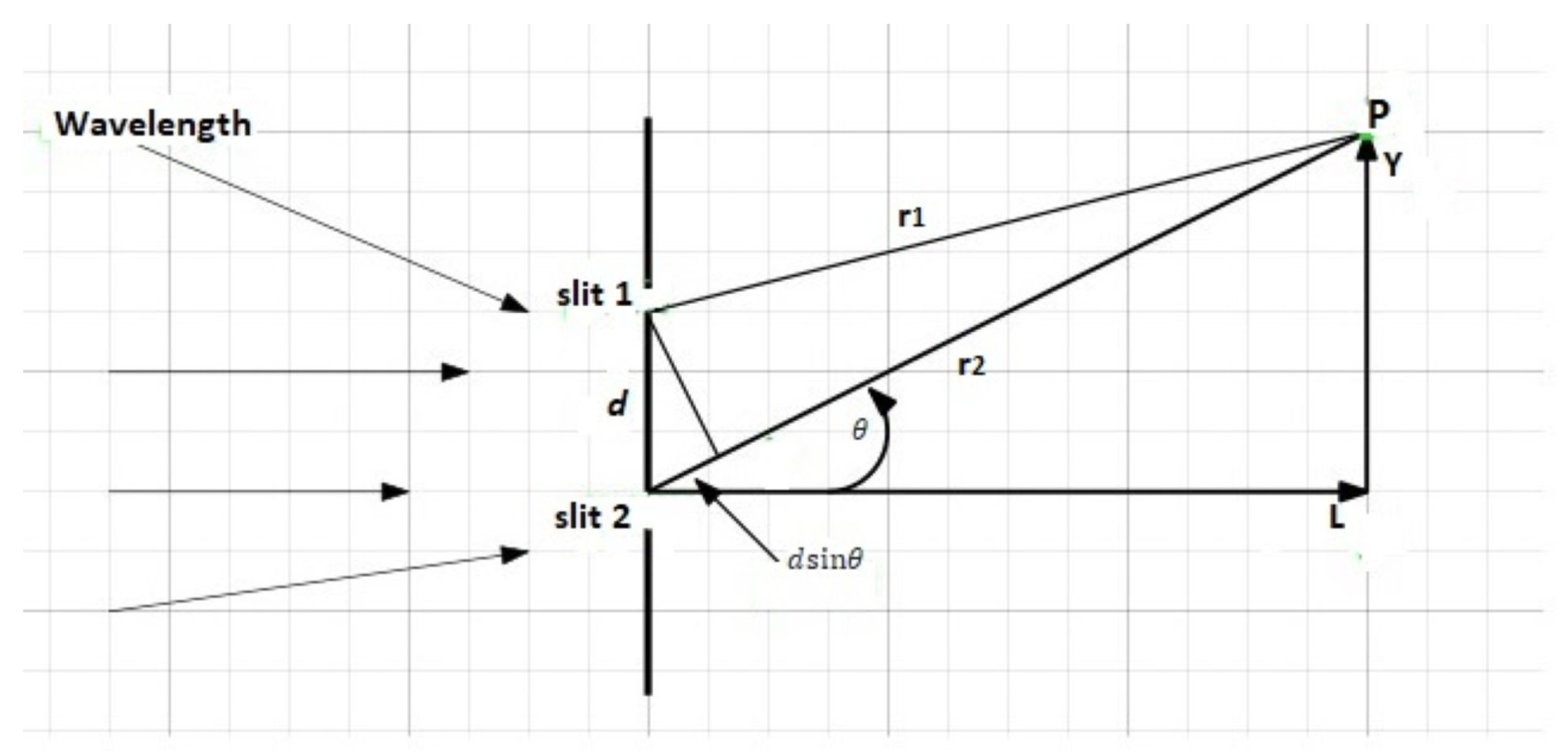
2. Diffraction Grating Theory

Diffraction grating is presented in Figure 1, where incidence and diffraction angles are measured from the grating normal to the beam; this paper keeps that principle. The sign convention for angles is shown by the plus and minus symbols located on either side of the grating normal for either reflection or transmission gratings.

2.1. Diffraction Grating Principle

A generic diffraction grating is a geometrical arrangement of reflecting or transmitting elements separated by a distance d that is related to the wavelength of light. These diffracting elements can be a pattern of transparent slits or apertures in an opaque surface, or a collection of reflecting grooves on a substrate. This paper focuses on the transmission grating due to aperture conditions. When monochromatic light is incident on a grating surface, it is diffracted into discrete directions. It is therefore normal to have a controlled diffraction that adjusts its pitch d in accordance with the incoming wavelength. A pitch d is the distance between adjacent regularly spaced grooves on a substrate a diffraction grating is made of [15]. Each grating groove can be viewed as an extremely small, slit-shaped source of diffracted light. For that purpose, we consider these slits, which are made of entrance and exit, as sources of the same characteristics in accord with the Huygens principle [16], without having a concern of a type of pattern, nor the incident signal. In analyzing the geometry of the photometer in this paper as in the literature, we make use of wavefront of the diffraction grating, considering it emanates from a surface of constant phase (Figure 1). The resulting grating equation governing the angles of diffraction from a grating of groove spacing d is given by [17]
m λ = d ( sin α + sin β ) ,
where m is an integer called the diffraction order, also known as spectral order, which, for a given wavelength λ , takes the values imposed by the constraint m λ d < 2 , corresponding to the feasible diffraction orders. The goal of the diffraction grating is to separate light beams within the available space into their wavelength components and direction. A measure of these wavelengths’ separation is known as dispersion, which can be spatial or angular.
The angular dispersion D expressed per unit angle can be written as [18]
D = δ β δ λ = m d cos β = sin α + sin β λ cos β ,
expressing the angular diffracted angle deviation of order m between λ + Δ λ and λ .
The linear dispersion L D , expressed per unit length, can be obtained by multiplying the angular dispersion and the focal distance f [19]:
L D = f D = f m d cos β .
To avoid dispersion, which is disturbing, the grating must be able to separate adjacent spectral lines of average wavelength λ ; this ability is known as spectral resolving power. The resolving power R is given by [18]
R = λ Δ λ ,
where Δ λ represents the limit of resolution, which is the difference in wavelength between two spectral lines of equal intensity that can be differentiated.
This expression in a planar diffraction grating with N grooves is written as R = m N , while the ruled width a of the grating is given by a = N d . Substituting yields [18]
R = a ( sin α + sin β ) λ .
The ability to resolve two wavelengths λ 1 and λ 2 = λ 1 + Δ λ depends not only on the grating, but on the dimensions and locations of the image plane and detector elements; the deformation and magnification of images are defined as resolution, noted Δ λ (nm). The resolution or the ability of a grating system to resolve nearby wavelengths is without a doubt more relevant than the resolving power, considering that it determines the image effects of the system, hence the bandpass of the signal importance. Bandpass B of a spectroscope is the wavelength interval of the light that passes through the exit slit or falls onto a detector element [18].
In the intensity graph against wavelength, the bandpass is empirically defined as the difference in wavelengths between the upper and lower frequencies in a continuous band of wavelength, an important estimate this paper intends to make use of in view of determining the geometry and evaluating the performance of our spectrophotometry. Mathematically, B is the product of the exit slit-width w and the reciprocal linear dispersion L D :
B = 1 L D w = w d cos β m f .
A spectroscope with a small bandpass can resolve wavelengths that are closer together than the one with a larger bandpass. The bandpass is made small by decreasing the width of the exit slit w, but at the expense of decreasing light intensity. In this paper, we suggest an intensity magnification and display unit optimization that achieve small bandpass and resolve images from microlevel down to nanolevel. The constraints intensity–slit-width are managed by an adapter that amplifies intensity and finds the required position of the display unit. For the display unit to exhibit nano- or micro-measurements, such charge-coupled devices (CCDs) are required. Recent studies have showed the possibility of nano-pixel measurements [19]. This paper anticipates on these measurements by suggesting such display unit elements.
Therefore, in this paper, we suggest the wave-front characteristics, from its emission by the exit slits of the diffraction grating, up to its presentation by the display unit, which are the spatial and bandpass dimensions meant for a spectrophotometry capable of detecting nanoplastics.

2.2. Generic Optical Field on the Display Unit
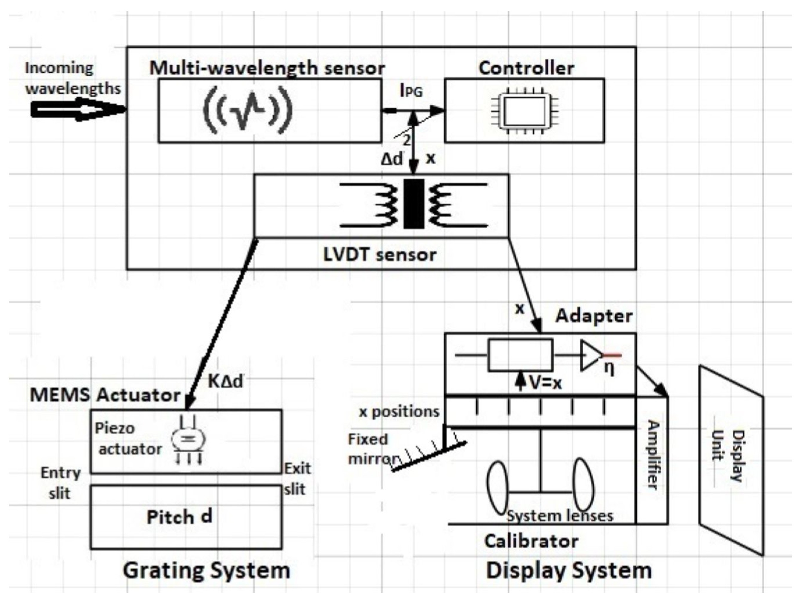
Let us consider an optical field A, its expression at r as shown in Figure 2 is given by
A = R e ( A 0 e x p ( i ( ω t k r ) ) ) ,
where k = 2 π λ , λ is the wavelength, which corresponds to the intensity I = 1 2 ε 0 ( R e ( A ) ) 2 which can be normalized without loss of generalities, with R e being the real part. Intensity becomes important when more optical fields are superimposed. Let us consider for simplicity two superimposed optical fields; the time-averaged intensity does not depend on the phases separately, but on their amplitudes and phase difference. This is shown in [18], where it was found that what makes the separate phases drop out is that the sum of two waves always has an overall, average phase, and a phase difference. The average phase combines with the time oscillation to cancel out each other, but the phase difference does not. Thus, in the following, we will focus on phase differences among sets of waves ni accordance with Figure 2.
Let d be the distance between any two slits of the grating surface, also known as pitch; λ is the wavelength. Since d is uniformed, the waves will be entirely in phase everywhere.
Let r 1 and r 2 be the distances from S 1 and S 2 to the point P of height y on a screen placed at L from the gratings with diffraction angle θ , as shown in Figure 2 and Figure 3. For a uniform separation d between slit S 1 and S 2 , the generic optical field at any distant point P on the screen is expressed as the sum of the fields produced from the two slits by linearity:
A p = A 1 + A 2 = A 0 e i ω t ( e i k r 1 + e i k r 2 ) .
The difference in path between both slits at P is given by Δ r = r 2 r 1 = d sin θ , which corresponds to a difference in phase of Δ ϕ = 2 π λ d sin θ , considering m = 1 . This phase has an impact over the intensity particularly over the point of the measure of that intensity P. To optimize the intensity on the display unit, this paper suggests the following controller.

3. Controller Unit

We consider a more elaborate arrangement of dynamic gratings separated from one another of distance d that is variable, as well as variable wavelengths emitted or transmitted from molecules and particles in a sample, and we analyze how to improve the image in terms of intensity at a certain point r from the slit. We suppose the orthogonality of the beam between any two slits, we evaluate the optical field on the screen with m = 1 , and assess the impact of the controller on that field. The controller exerts several functions after sensing the emitted/transmitted wavelength λ . To determine these functions, the focus of this paper, we make use of the system given in Figure 3.
Our aim is that any emitted or transmitted wavelength characterizing a sample must be detected by the proposed system. This requires most components not to be wavelength-bound, or better wavelength-dependent. Such a system is made of the following:
  • A dynamic grating actuated by a MEMS piezoelectric actuator, which, through instruction from the control unit, allocates the required slit-width by varying the pitch with a displacement Δ d that is meant for a specific incoming wavelength. That incoming wavelength is diffracted with an angle θ and refracted towards the display unit.
  • A display unit, which, under instruction from the control unit, positions the mirror in accordance with the specifications from the controller, such that the diffracted wavelength undergoes a reflection that concentrates the maximum signal in a required geometric etendue to the screen.
  • A controller that controls the whole system. The aim is to discard wavelength-dependent devices, and to optimize the intensity on the display unit for a better and accurate imaging, while minimizing the negative impacts from the diffraction grating up to the display unit.
In the following, we describe the functions of each component and give the mathematical expressions of those control functions. The principles of the required devices as well as the deployment of our system are given in Section 4.

3.1. Controller Devices and Functions

We give in this section the description of the necessary devices that execute the controller’s functions with wavelength-wise flexibility, or not. More details regarding these devices’ principles are given in Section 4.
The signal from the sample to the display unit is managed by a multi-sensor controller system which executes them through the adapter–calibrator on one hand, and on the other hand, via an MEMS.
The multi-sensor controller is a compound sensor made of a multi-wavelength sensor capable of sensing Ultraviolet (UV), Visible Light (VL), and Infrared (IR) radiation. The multi-wavelength sensor carries out its actions through a secondary sensor that transforms the wavelength sensed into an electrical signal meant for the adapter and the MEMS. More details on these devices are given in Section 4.
The adapter, not directly wavelength-dependent, transforms this electrical signal into a position x that is automatically switchable, and assigns through a controlled switching in accordance with the Look Up Table (LTU) of the sensor processor the amplification required η to the diffracted signal. The adapter carries out its actions automatically and or through a calibrator as provisions for image improvements, since provisions are made for adjustments through the calibrator. This adapter is detailed in Section 4.
The calibrator is made of a reflective fixed mirror with reflection angle r directing the beam with angle r r e f that aims to concentrate the signal on a required portion of the screen. It is worth mentioning that the mirror moves horizontally in accordance with the switch’s predetermined position x on top of which it is fixed. The position x that is meant for the incoming and then diffracted wavelength, allows the mirror to maximize the signal’s geometric etendue on the screen. Contrary to the fixed mirror that interacts with the incoming diffracted wavelength radiation with the aim to concentrate the signal on the smallest etendue possible, the system lens, instead, is a necessary option for the human naked eyes’ visual aid during the reading out from the display unit, and to mitigate dispersions through the focal distance in accordance with Equations (2) and (3).
The switch associated with the calibrator operates automatically in accordance with the adapter’s potential values translated into spatial positions, and can also be adjusted by the calibrator leveler. The switch is a spatial switch that takes on the set of values x as per adapter-given parameters. More on it is given in Section 4.
After reflecting on the mirror and prior to reaching the display unit, the signal is magnified by an amplifier according to the values of η and the LTU-associated reading from the adapter, that finds the proper signal level required to increase the number of electron extraction on the etendue of the display unit. Therefore, the function of the adapter is defined by l = f ( x , η ) , with x the optimal position determined by the calibrator, η the optimal intensity gain, and l the manipulable leveler belonging to the calibrator.
The display unit, which is wavelength-dependent, is an image sensor represented by an array of photosensitive pixels. Each pixel is made of photodiode and a potential well capacitor, whereby the first, upon the amplification of the refracted signal by a Semiconductor Optical Amplifier, generates the flow of photoelectrons that are collected by the potential well, where a single image will be formed when the required number of photoelectrons is reached. The representation of the entire array creates a sequence of images that are red out by a charge-coupled device (CCD). A CCD image consists of a small rectangle of arrays of cells known as pixels. To each pixel is assigned a number called Analog-to-Digital count (ADU-count) which is proportional to the brightness of the image at the location. It is worth reminding that in terms of dimensions, 1 cm corresponds to 37.8 pixels, and that as the technology evolves, nanopixels are acquiring momentum. A pixel size of 1.2 μ m has been also reported as well as nanopixel size. One (1) nanopixel corresponds to 300 nm× 300 nm of size [20].
The MEMS is on the diffraction grating side and not directly wavelength-dependent. However, through it, the controller ensures that an incoming wavelength λ emitted or transmitted from the sample is accommodated by triggering the actuation that causes the pitch tunability conferred to the grating by the MEMS. In fact, the MEMS yields the required slit-width by modifying the pitch in accordance with the MEMS function f ( λ , Δ d ) , with Δ d being the added to or subtracted from d (this analysis adds) as per controller instruction. The MEMS does so through its piezo-actuation capability. More details on these devices are given further in Section 4.
Therefore, the objective of determining the controller’s functions f ( x , η , Δ d ) is to optimize the intensity for a given number of slits that improves clarity, brightness, sharpness, and accuracy on the display unit. This is achieved by transforming most of wavelength-dependent devices into wavelength-independent ones, and by concentrating the maximum of light in the required radius called etendue. Making that etendue as small as possible to achieve a smallest pixel radius increases the sharpness and accuracy necessary to detect nanoparticles, Hence the following function characterization.

3.2. Characterization of the Controller Functions

The role of the controller is to detect through sensor any wavelength emitted or transmitted by the sample, to provide adjustment means that optimize the position and the signal on the display unit through the adapter, and to adjust the grating pitch tunability to accommodate the sensed wavelength through the MEMS actuator.
Assume a point at a distance r from the grating slit, r is adjustable for an average wavelength-maximum intensity such that the adjusted point on the display unit becomes r = r ¯ + l , l being the adapter function that optimizes the intensity and the display unit position, r ¯ the actual average ( r ¯ = r 1 + r 2 2 ) when compared to r 1 and r 2 , which are the distances from both sources, the calibrator function l = x ± i η k a complex number made of the position x that adapts the display unit etendue to each incoming wavelength, and the gain component (according to the sign (±)) that amplifies or attenuates the intensity. In the following, we will only amplify the signal. Therefore, the optical field is given by
A p = A 0 e i ω t ( e i k ( l r Δ r 2 ) + e i k ( l r Δ r 2 ) ) A p = A 0 e i ω t e i k r e η e i k x cos ( Δ r 2 ) A p = 2 A 0 e i ω t e i k r e η e i k x cos ( k Δ r 2 ) .

3.2.1. Adapter Intensity of the Field on the Display Unit

In the following, since we focus on the exit slit of the gratings and for simplicity, we omit α in Figure 3, hence the results given as functions of the entrance slit of the gratings, with the aim to accommodate in the future the sample’s reaction that can be transmission, refraction, scattering, or absorption.
From Equation (9), let I 0 = ( A 0 e i ω t e i k r ) 2 be the intensity at the diffraction grating output slit; the intensity of the field at P as shown in Figure 3 is given by
I p = 4 I 0 ( e η cos ( k Δ r 2 ) ) 2 = 4 I 0 ( e η cos ( k x ) cos ( π d λ d sin θ ) ) 2 .
From Equation (10), the condition of coherence imposes λ d . If this condition seems possible, it is difficult to realize it in an actual system. It requires that we proceed with another approximation to reach this quasi-coherence while magnifying the intensity, bearing in mind that Δ ϕ 0 as θ 0 . The intensity at P becomes
I p = 4 I 0 e η cos ( k x ) cos ( Δ ϕ 2 ) 2 .
Imposing as the number of slits becomes large the difference of phase condition Δ ϕ 0 and considering the power resolution of the diffraction grating a = N d , where N is the number of slits d distant between one another, the superposition of the N slits, and exploiting the expansion series of cos ( Δ ϕ ) when Δ ϕ 0 on the optical field, this intensity becomes
I p = 4 I 0 e 2 η cos ( k x ) sin ( N Δ ϕ 4 ) 2 sin ( Δ ϕ 4 ) 2 .
The coherence in Equation (12) can be obtained if according to Figure 3, y L sin θ , and Δ ϕ 0 when y 0 , then the 1 4 normalized intensity can be as follows:
I p = I 0 e 2 η cos ( k x ) N 2 .
More explanation about y is given further in Section 4; however, we would like to outline here that there could be a problem when N . In that case, the system is not able to achieve an allowable range for the display unit. This justifies the role of the adapter in preventing this situation from occurring, as long as cos ( k x ) < 1 . The advantage is that, instead of limiting the number of slits, it is better to optimize them, as we will see in the performance (Section 4), which allows for the improvement of the image.

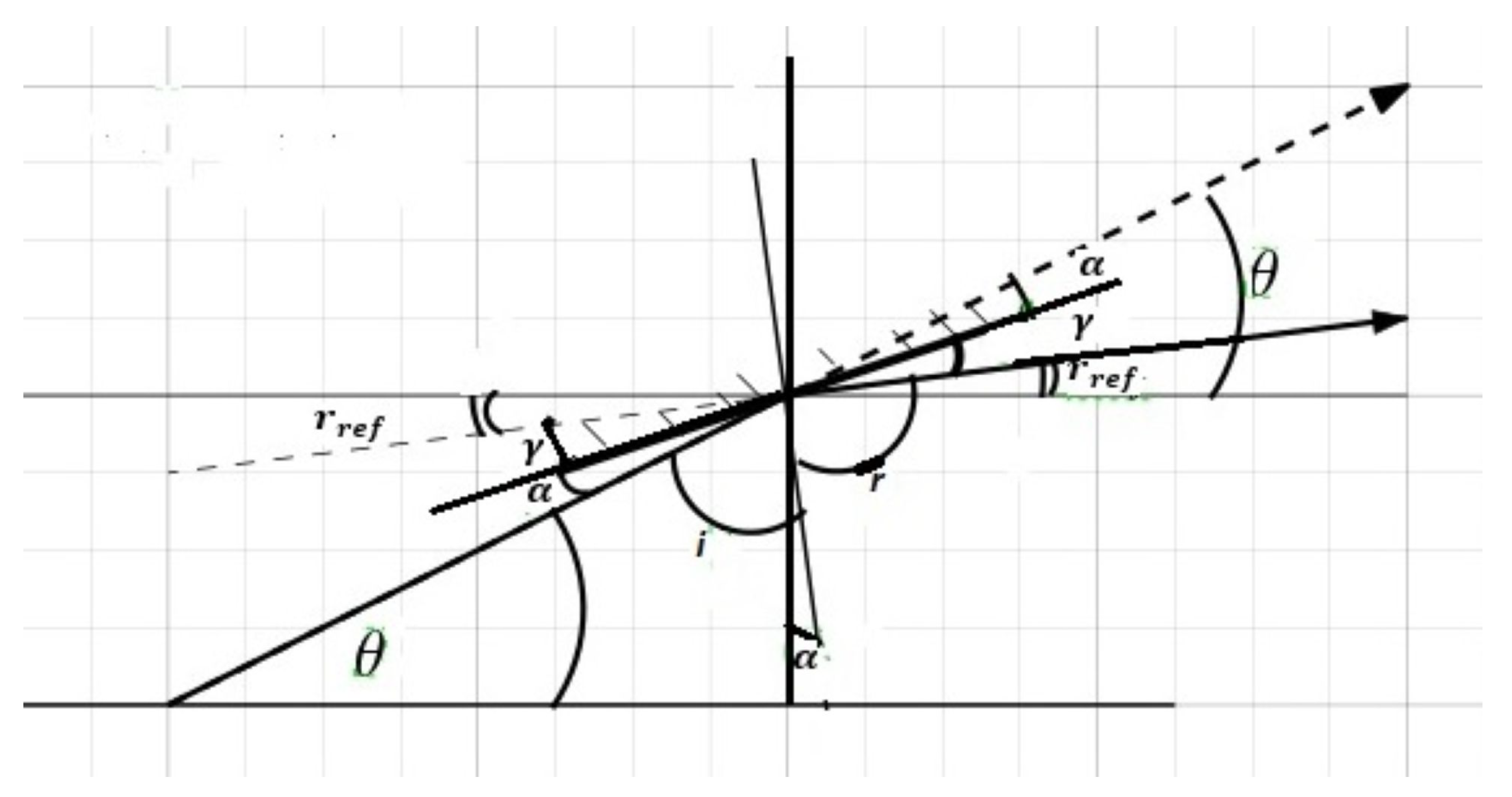
3.2.2. Calibrator Mirror Characteristics

The adapter through the calibrator makes sure through the reflection on the mirror angle that all the optical signal falls within the geometric etendue of the screen, the screen being positioned according to the measure x. If we consider that the surface seen from the solid angle is approximated to the etendue G, and the reflection angle is the angle of the summit of a cone where the entire etendue is seen, the angle of refraction is given by
r r e f = c o s 1 ( 1 G 2 π x 2 ) ,
x being the calibrator adjustable distance of the display unit, with r r e f being the reflection angle formed by the reflected signal taken from the horizontal axis.
The mirror is characterized by an incident angle i, the reflected angle r, and assuming that the system is in the vacuum, the mirror is inclined from the horizontal axis by an angle r r e f + γ , which, according to Figure 4, is such that
i = r ; r r e f + γ + α = θ ; i + α = π 2 ; r + γ = π 2 ; r r e f + γ = i + θ π 2 ; θ + ( i α ) = π 2
Consequently, these angles nullify the scattering angle, allowing the remapping of images on the charge-coupled devices (CCDs). Such provisions in the calibrator allow an increase in accuracy and sharpness on the display unit, since each CCD involved will convert more photons into electrons and remap the entire signal in a small number of CCDs.
From Equation (12), by considering Δ ϕ small, we can write
I p = 2 I 0 e 2 η sin ( k x N k Δ ϕ 4 ) + sin ( k x + N k Δ ϕ 4 ) Δ ϕ 4 2 .

3.2.3. Display Unit Etendue Optimization

The optimization of Equation (15) is achieved if the following condition holds:
sin ( k x N Δ ϕ 4 ) + sin ( k x + N Δ ϕ 4 ) = | 2 | .
A solution for the condition above to hold requires that
k x N Δ ϕ 4 = ( 2 n + 1 ) π 2 k x + N Δ ϕ 4 = ( 2 n + 1 ) π 2 .
The solutions of this system of Equation (16) are such that x = ( n + n + 1 ) λ 4 or x = 0 as long as N Δ ϕ 4 = ± ( 2 n + 1 ) π 2 , and the ( n , n ) combinations allowed in n + n + 1 yield the following values of x:
x = 0 , ± λ 4 , ± λ 2 , ± 3 λ 4 , ± 5 λ 4 , ± 3 λ 2 , ± 7 λ 4 , ± 9 λ 4 , .
This set represents mathematically the different positions of the adapter handled by the calibrator that optimize the etendue on the display unit as well as the pitch variation on the gratings. It is therefore important to determine accordingly the diameter D e of that etendue and to characterize f ( λ , Δ d ) .
Furthermore, from Figure 3, let D e be the diameter of the etendue and y the height from the center of the etendue such that D = 2 y .
tan θ = y 2 x = y L yields the following adjustable position once the controller senses λ :
L = 2 x = ( n + n + 1 ) λ 2 x = ( n + n + 1 ) λ 4 .
Furthermore, tan r r e f = y x . For small angles, tan θ = θ = sin θ ; similarly, tan r r e f = r r e f = sin r r e f and any other angle. This allows us to write accordingly the characteristics of the mirror: r r e f = 2 i + θ π . For a fixed mirror angle r r e f + γ = Θ , the relation incidence angle i and the diffracted angle θ are such that i = π 2 + Θ θ , leading to r r e f = 2 Θ θ = tan r r e f = tan 2 Θ tan θ .
Furthermore, through geometry, tan θ = y 2 x = y L and tan r r e f = y x . This leads to 2 Θ y x = θ = y 2 x or y = 2 x ( tan Θ tan θ 2 ) . It comes that the diameter of the etendue, which is the circle impacting the etendue, as defined by x, is given by
D e = ( n + n + 1 ) λ 2 ( tan Θ tan θ 2 ) .

3.3. Grating Pitch Variation Evaluation

Equation (18), or the diameter of the etendue D e , gives us the maximum size of the image on the display unit. It is therefore important also to maximize the intensity of the signal, and this is accomplished if the controller imposes a limit in positioning the mirror and the system lenses via the adapter–calibrator when N is large. This implies then the following cases to x:
x = lim 0 , ± λ 4 , ± λ 2 , ± 3 λ 4 , ± 5 λ 4 , ± 3 λ 2 , , N small x = lim Sup / Inf 0 , ± λ 4 , ± λ 2 , ± 3 λ 4 , ± 5 λ 4 , , N .
Furthermore, from the system of Equation (16), one finds that
N d λ sin θ = n n , n n ,
and when comparing Equations (17) and (20), we get the following equation characteristic of the grating pitch function S = f ( λ , Δ d ) :
N d 4 sin θ + x = ( 2 n + 1 ) λ 4 .
Once the controller senses the emitted/transmitted wavelength λ and reads x from the adapter, it switches the necessary current that circulates in the MEMS to create a force that causes the pitch to vary from d to d + Δ d . This yields a displacement Δ d expressed as
Δ d = 4 x ( 2 n + 1 ) λ N sin θ d , Δ d w 2 .
The design and choice of the type of MEMS must meet the requirement of producing a force F such that Δ d = F K , with K being a spring constant. The force F must be applied in respect with the slit-width w such that Δ d w 2 . This suggests also a multi-level of energy source for F, which is not the focus of this paper. One can find the multi-level source treatment in [21].

Derivation of the Classical Spectrophotometer

The flexibility of the system can be achieved by considering the first minimum of Equation (25) is at N π d y 2 λ L = π and x = 0 .
Since x = 0 reverts to the classical solution, it is important to provide the etendue using that solution for comparison purpose. The width of the maximum image on the display unit is given by
Δ y = Y m a x Y m i n = 2 λ L N d .
Furthermore, the positioning distance of the display unit from the slits is at L = N Δ y 2 ( d λ ) .
Since θ is small, we can approximate L to the focal distance f; that is, f L .
Furthermore, the linear dispersion is combined with the diffraction grating to resolve details of the spectra without ambiguity; therefore, it can be written as
L D = 10 6 c o s β m N L B .
This gives us the geometric etendue G of the display unit, which characterizes the display unit ability to accommodate the signal. The etendue is given by
G = m G A N B 10 6 L B .
where G A is the geometric etendue at the entrance slit in mm 2 , B is the bandpass in mm, L B is the focal distance in mm, m is the mode or order of gratings. Clearly, the etendue on the display unit classically designed depends mostly on the bandwidth and the entrance slit etendue G A .
This etendue G is managed differently by the adapter, which is determined in accordance with the image size defined by Equation (18).

4. System, Results, and Simulation

4.1. System Implementation

For the system to operate, it requires a source that excites the molecules in a sample, and these molecules and particles emit or transmit wavelengths which interact with the detection system. Though we focus on Infrared (IR) radiation, the universality and multi-scale require a range of sample wavelengths to span from Ultraviolet, up to IR through Visible Light (VL). It is therefore necessary to bring light on such a range.

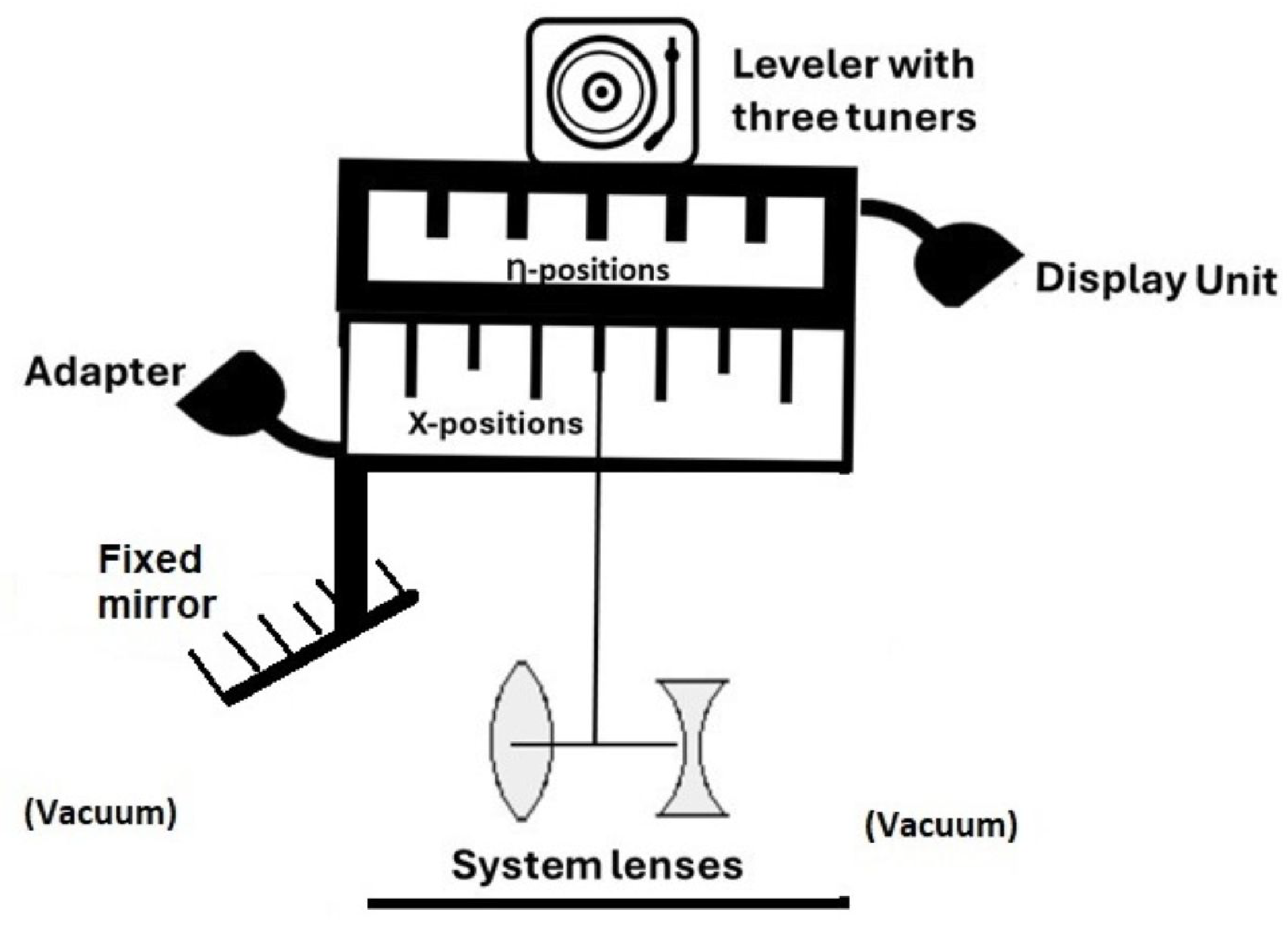
4.1.1. Source and Sample Characteristics

Mentioning the sample, it must be able to support Raman/fluorescence, Photoluminescence, and IR spectroscopy operations, scattering, emitting, or transmitting a variety of radiation ranging from UV through VL, up to IR radiation, as per universal spectroscopy and multi-scale conditions. This wide range comes from several assumptions: the sample is assumed to have microplastics, their degraded forms into nanoplastics, and their probable retentions of nanoparticles and pathogens. Pathogens with capability of penetrating biological tissues are characterized by 20 nm wavelength energy, hence a [20–110] nm range suggestion. Furthermore, when IR radiation excites molecules in a sample, they can undergo Stokes shift, which results in longer wavelengths, or Anti-Stokes shift that yields shorter wavelengths, hence a [700–1700] nm wavelength suggestion. Furthermore, we have assumed that other particles in the sample react to UV-VL from the sun or other environmental emissions reaching the sample, but are likely to undergo the same Stokes shift dynamism, which results into [120–650] nm, hence a universal spectrometer/photometer capable of detecting these ranges of wavelengths, from vibrational with absorption or scattering.
These wavelengths emitted or transmitted by the sample require the source energy with radiation λ to excite the molecules in the sample. These excited molecules can further experience Stokes shift to produce longer wavelengths such as 1700 nm; or Anti-Stokes shift with the introduction of the phonon thermal conductivity, for instance, which can provoke the emission of 20 nm (see [21]). Furthermore, we can also choose the source to provide multi-level radiation. In that case, the source must be able to trigger multiple-level emission or transmission from the sample. However, it is also important to mention that the sample emission is totally independent of the source radiation; that is, unlike during a dynamic Stokes Shift described above that allowed for a [20–1700] nm emission, the source multi-level radiation having nothing to do with the molecules’ emissions. Hence, we propose a dynamic laser source for such a source.
A dynamic laser is a laser whose wavelength of operation can be altered in a controlled manner to meet the needs of different applications. Furthermore, known as tunable lasers, we propose diode lasers for our application. It is worth mentioning that among the laser’s tunability schemes, we propose the mechanically tunable lasers, since they provide greater flexibility for applications requiring precise control over the wavelength, such as spectroscopy with multi-level energy. More details on tunable diode lasers for spectroscopy can be found in [22], but we suggest a laser operating up to extreme UV, as the one proposed by [23], that allows us to operate within our target range [200–1550] nm. To achieve this wavelength range, frequency conversion, as proposed by [24], which aligns with “The Harmonic Generation Technique” that doubles, triples, or quadruples frequency, is used in combination with the technique of tunable diode laser. Besides the Harmonic Generation Technique combination of diode lasers, the combination of different diodes can also be used.
In addition to the sample manipulations above that yielding [20–1700] nm from a [200–1550] nm source, it may happen that the radiated laser energy is high and damaging to the sample’s particles or molecules; in such a case, the flux of the emitted source radiation may be reduced via an N-power splitter, as in the multimode photonics presented in [21,25].
One of the source characteristics above is then chosen to excite the sample, which emits or transmits wavelengths that need to be detected by our system.

4.1.2. System Description

The system proposed must be able to align with the new generation of universal spectro-/photometers. Therefore, the components described are all taken from the current ongoing developments and improvements in micro-/nanotechnology. The system is set up such that pivotal components are not directly wavelength-dependent due to the universality system condition, which consequently makes sure of the quasi wavelength-independence of all other components involved, while ensuring that the proper wavelength reaches the display unit, in accordance with Figure 5.
The system is made of a grating system and a display system, both managed by a multi-wavelength sensor generally known as multi-sensor or compounded sensor system.
The multi-wavelength sensor system is made of a first sensor which is of light sensor type or of multi-wavelength optical sensor type, sometimes referred to as a wavelength test sensor, and it is directly wavelength-dependent. For universality and multi-scale purposes, it must be sensitive to each vibration, emission, and transmission coming from a sample in hands, which is supposed to be of [20–1700] nm wavelength signals. It does that by measuring the potential depth of each incoming transmission or emission as well as any vibration from the sample, exploiting a spark timer principle. The multi-wavelength sensor system was already mentioned based on its potential depth importance in [26]. More details on the wavelength range and both techniques are given in Section 4.1.2.
This multi-wavelength sensor outputs an electrical current function of the wavelength and the potential well characterizing the sensor. This current is processed by a microprocessor of the controller, which determines the pitch variation Δ d (22), and a variation of position x (17), outputting therefore two different positions ( x , Δ d ) as secondary physical properties meant for a passive sensor known as Linear Variable Differential Transformer (LVDT), which is a sensor of position type.
The LVDT is a passive sensor that measures position and produces electric energy. It is worth noting that there are two secondary LVDTs, the first passive LVDT sensor; each, through inductance variation, produces a voltage, on one hand, that is proportional to Δ d ( U Δ d ) for the MEMS actuator on the grating side, and on the other hand, a voltage that is proportional to x ( V x ) meant for the adapter on the display unit side.
The grating system side is made of a MEMS actuator, which is quasi wavelength-independent, as it is fed by the secondary LVDT sensor. Our MEMS actuator’s type is a piezoelectric actuator that converts the electrical signal from the LVDT into a precisely controlled physical displacement Δ d , conversion made possible by the transducer that converts electrical energy into mechanical displacement based on the piezoelectric effect that characterizes its mechanism; that is, to transform the voltage into a displacement materialized by U Δ d or function f ( Δ d , U ) , that also modifies the slit-width and, consequently, the bandpass.
The display system is also fed by the secondary LVDT sensor, which is sensitive to the variation of the position x and passes its output to the adapter. The quasi-wavelength-independent adapter, instead, is made of a potentiometer that takes on the LVDT output, the divided voltage V x passed on to the calibrator, and an amplifier whose output e x p ( 2 η ) is the product modulated with the incoming wavelength intensity towards the screen.
The calibrator, which is alternatively a hand tool, is automatically connected to the adapter. It is made of a leveler through which it finds the proper coefficient of proportionality emanating from the voltage divider ( V x ), a mirror that is fixed at its edge, and a system of mobiles lenses suspended at the end of a thin insulation and transparent-like material, all enclosed and freed of any external radiation, namely, in a vacuum. The thin material is in turn supported by a switch that takes on adjusted x positions from where the system lenses can be positioned accordingly to optimize the image for the naked eye. More details are given in the next section; that is, the details of the setup given in Figure 5 in terms of principle and implementation of its components are given in the following section.

4.1.3. System Component Principles and Implementations

A. 
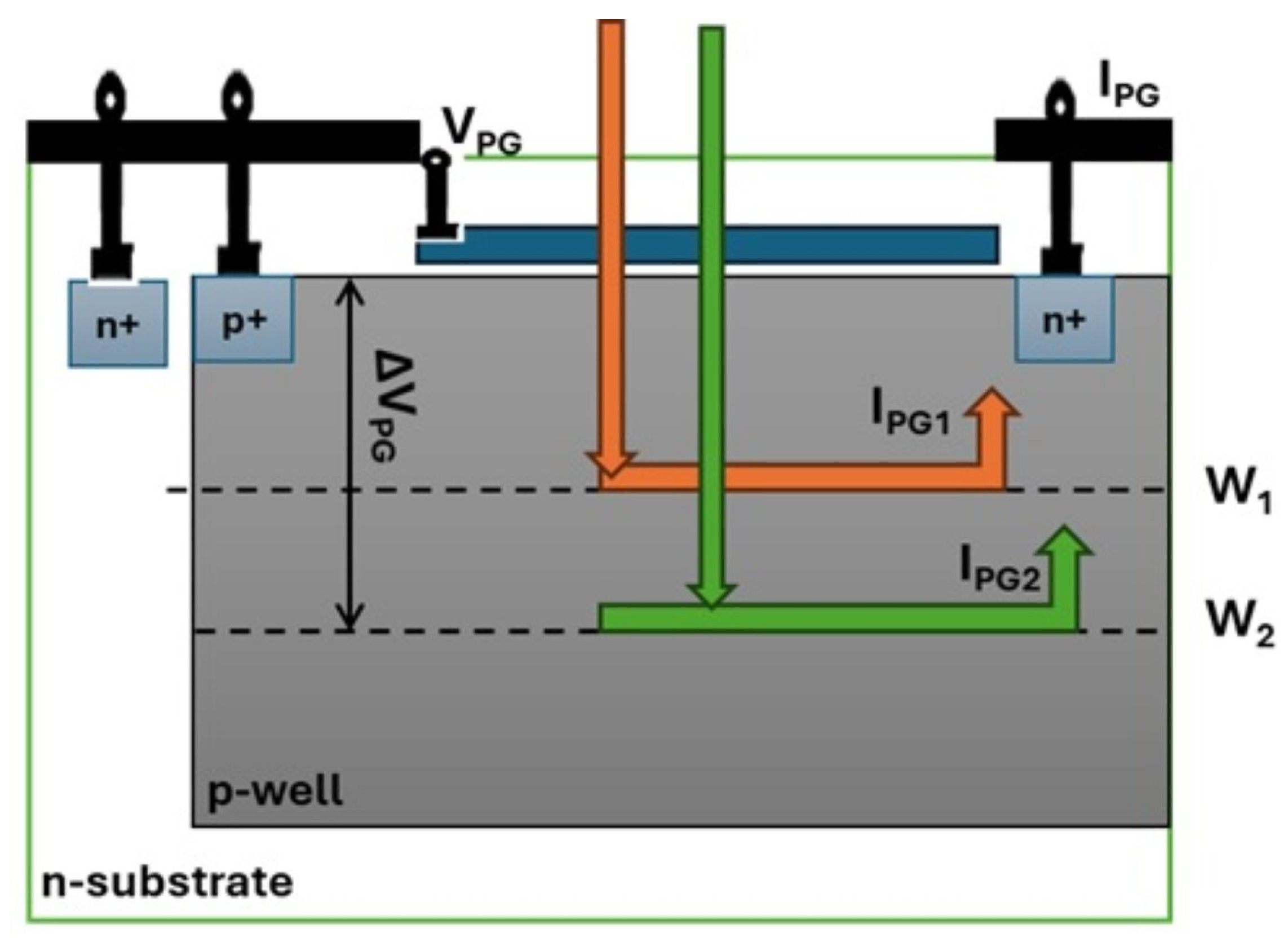
Multi-wavelength Sensor
The primary sensor is a multi-wavelength sensor that reacts to the vibration of particles and the incoming wavelengths. It is a filter-free sensor on n-type silicon (Si) substrate with a p-well layer formed on the silicon substrate similar to the one reported in [27], but with modifications regarding the impurities and signal conditioning. Instead of modifying the sensor, like achieved in [28], due to the characteristics of the peripheral circuit potential issues owing to the voltage changes that are applied to the n-substrate, we proceed with signal conditioning by making sure that the voltage falls within the appropriate wavelength range that the peripheral circuit can cope with. In that way, each individual wavelength produces the intensity I = f ( λ ) for each incoming wavelength. A technique of n or p-wells on the silicon-based impurities substrate is applied to ensure that I = f ( λ i ) I = f ( λ j ) for any i j leaning on a potential depth W of a single well, which is achieved by the photogate technique, as in [27,28], hence covering the broad range of [ 20 1700 ] nm radiation capability.
The photogate technique is based on a spark timer principle that detects with high accuracy a position, velocity, acceleration, or vibration by collecting information exactly at the time a specific event occurs; that is, time t i . The photogate therefore captures multiple wavelengths, leaning on the photogate spark timer mode t i = λ i c and the intensity of each incoming wavelength. The light irradiated on the silicon surface is absorbed inside the silicon to generate electron–hole pairs. Our multi-wavelength sensor being a single-well structure on an n-type silicon substrate, it adjusts the potential depth W by controlling the photogate voltage ( V P G ) based on each incoming wavelength. Essentially, each incoming wavelength influences the current produced, and current is then processed by a separate circuit that adjusts the photogate voltage output accordingly. The photoelectrons that are generated on the surface side of potential depth W were collected by the n + diffusion layer as an electric current from the readout electrode to yield the photogate intensity I P G . Figure 6 shows two wavelengths separated by the multi-wavelength sensor, each one with its own photogate intensity I P G 1 and I P G 2 and wells, respectively.
The current generated is given by
I P G = I 0 n e S λ h c P g ( W ) ,
where I 0 is the light intensity reaching the sensor surface S, P g ( W ) = 1 e x p ( α W ) is the characteristic of the substrate and α the substrate (silicon here) absorption coefficient, I P G is the current towards the secondary sensor.
To implement such a multi-wavelength sensor, we suggest the same filterless wavelength sensor of n-type silicon substrate to which are added Germanium impurities with the aim to accommodate the wavelength range [20–1700] nm, since it is shown that silicon-based photodiodes with specific impurities enhance its wavelength sensitiveness from UV to IR [29]. Germanium (Ge) is able to detect all compounds that interact with the UV and VL spectra, and as an impurity, it brings that edge to our silicon. The technique takes advantage of the thin thickness of the Si and the wavelength-dependent absorption coefficients of both Si and Ge. When put together, both photodetectors yield a sharp contrast in photon-generation rate to each radiated wavelength, resulting subsequently to a different photocurrent. To determine the broad range from deep Ultraviolet (265 nm) to near-Infrared light (1550 nm) the one-to-one ratio of wavelength–photocurrent expressed through monotonic function was used by [29], range measured from applying the stacking of two photodetectors technique. As the changes in voltage can affect the peripheral circuits, to make sure that the changes in voltage do not disturb the operation of the peripheral circuit, provisions like noise mitigation can be be adopted, but this paper proposes the photogate voltage V P G range predetermined to accommodate all possible voltages, and the output channel is treated like in [30].
To make sure that wavelengths from the sample reach the multi-wavelength sensor as emitted or transmitted, we suggest to use the media of the optical rectangular waveguides with low-refractive-index contrast in accordance with the number of wavelengths that can be detected. For example, we can make use of two ranges: the range [265–1550] nm of [29] for emissions and transmissions, and { 30 , 50 , 70 , 90 , } nm of [31] for vibrations in the range [20–110] nm, while keeping the principle of a multi-wavelength sensor generating a current I = f ( λ ) from any λ , as described.
B. 
Controller
The sensor’s controller is a microprocessor made of specialized software and hardware to acquire, process, and analyze spectral data. The hardware is based on a FPGA chip with the sampling device and the LTU working under the synchronized clock at the frequency determined by the spark timer. This control system allows the spectrophotometer and the spectrometer to work in conjunction. The qualitative analysis is carried out by the spectrometer, while the quantitative analysis is executed by the spectrophotometer. This data analysis is carried out by software packages that are designed for acquiring, processing, and analyzing data from the multi-wavelength sensor. Among them, one can cite the customized software packages such as the Pulse Multi-LED absorbance detector to allow even the processing of deep UV radiation, or any data acquisition software, such as SoftMax® Pro 7.3. These software packages operate under a management software suite platform that has a friendly user interface, assuming good memory and processing capability of supporting conventional machine languages (C++ or Python) for prediction using machine learning.
The main operation of data acquisition from the controller is to extract λ from I P G according to
λ = h c I P G I 0 q S P g ( W ) ,
where q = n e , allowing through computation to calculate the changes in x and in Δ d as indicated in Equations (17) and (22), and to determine the potential depth associated with the number of electrons displaced through the 2 W = q ε 0 . The calculated values are passed on to the respective ports i feeding the secondary sensors.
To each controlled circuit i leading to the secondary sensor is associated a delay element T i which is measured from the previous signal λ i 1 . That is, T i = i λ i 1 c to allow the secondary sensor to process the sensed λ i wavelengths. For N grating slits, there are N + 1 delay elements, N + 1 indexed lines towards the LVDT of the grating towards the MEMS (two MEMS for one slit), and N indexed lines towards the LVDT for the adapter–calibrator, while the amplifier will be having N + 1 to indicate one control channel feeding the display unit. All theses N + 1 index lines are managed through the Look Up Table (LTU) within the controller for a better controlled system.
C. 
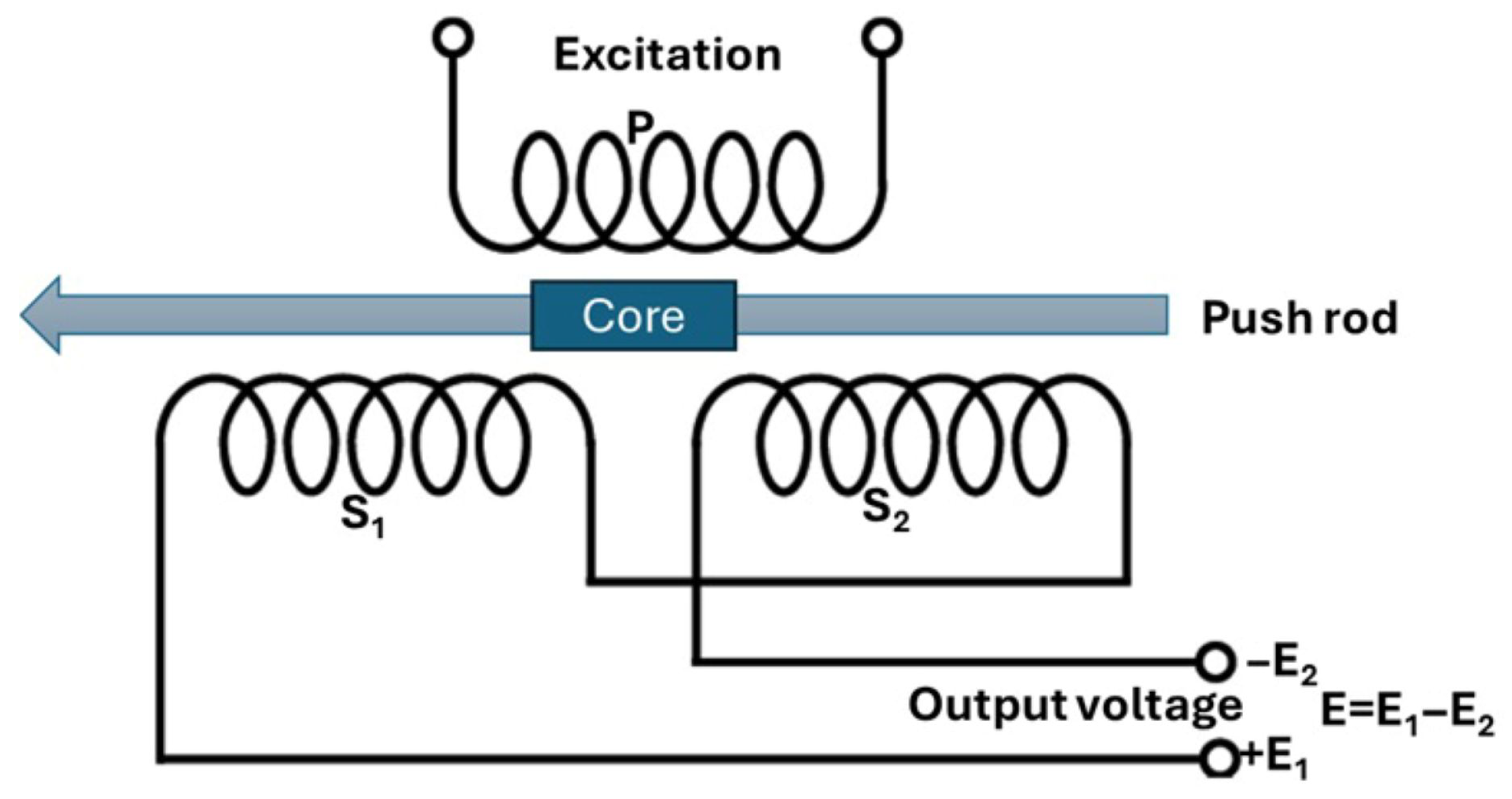
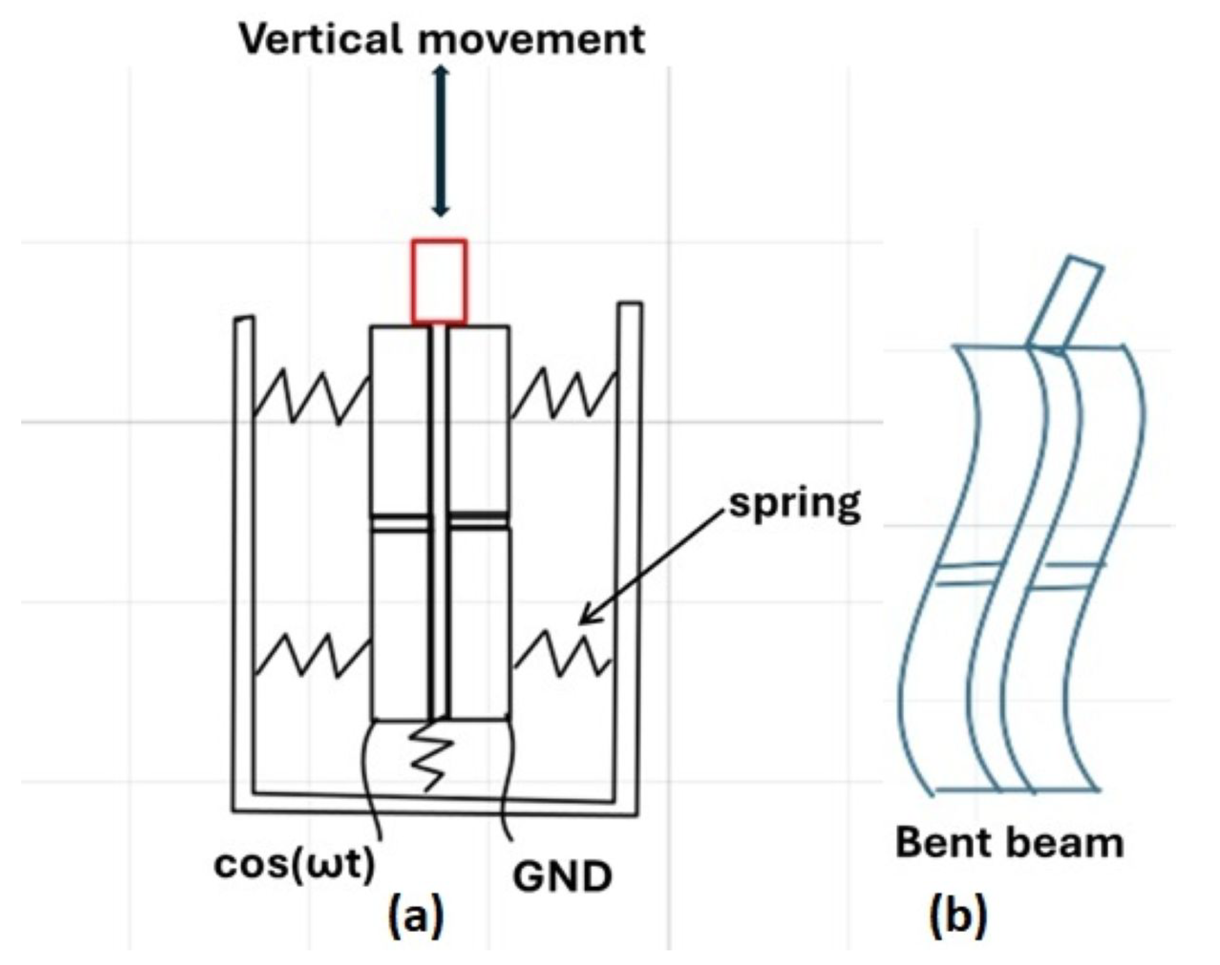
Linear Variable Differential Transformer Sensor
A Linear Variable Differential Transformer, or LVDT sensor, is a passive sensor which is sensitive to the variation of the positions (position type) x and Δ d determined by processor from the primary sensor. The LVDT sensor leans on Faraday’s law of electromagnetic induction that states that the electrical power in the network induction circuit is proportional to the rate of change of magnetic flux in the circuit.
In principle, the primary winding P of LVDT is connected to the AC power supply, The alternating magnetic field is produced in the primary winding, which results in the induced EMF of both secondary windings S 1 and S 2 . To translate the displacement into the voltage between S 1 and S 2 , there is a push rod supporting a ferro-magnetic core that, as it moves off-center of both secondary windings due to the displacement of the rod, generates a difference E 1 E 2 that is proportional to the displacement of the rod (see Figure 7). To displace the rod, the port connecting the rod ensures its vibration through the extracted λ signal expressed as s ( t ) = c o s ( 2 π f ( t x c ) ) . The related LVDT outputs accordingly V x .
The same principle exists for the signal toward the LVDT linked to the MEMS actuator, but with the difference that the extracted λ signal is expressed as s ( t ) = c o s ( 2 π f ( t K Δ d c ) , and the sensed position is multiplied and modulated by K, such as the voltage at the input of U K Δ d .
To implement these LVDTs, two secondary LVDTs are required (though only one is represented with two ports), each one of them being a simple transducer as simulated in [32], but due to the sensitivity to the variation of wavelengths as well as the ambient temperature which can generate heat, disturbing electronics, we are suggesting a similar implementation, as presented in [24], due to its resilience to the variations of excitation (inputs) signals and harsh environment as well as its high sensitiveness to ensure consistent and accurate measurement of linear displacement like the one in [33]. The output of one LVDT is connected to the MEMS actuator, and the other one to the adapter; both are controlled, in accordance with the controller’s LTU.
D. 
MEMS Actuator
MEMS grating’s typical structure consists of an array of parallel reflective grating grooves suspended by spring flexures, and implemented on a piezoelectric membrane that deforms when a voltage is applied on it. It is not triggered by the wavelength, but the voltage. The source voltage is connected in parallel to those parallel MEMSs such that each one actuates its own pitch. The applied voltage allows the grating array to evenly spread out and consequently change the grating pitch. Provisions must be made to differentiate the actuation level through voltage drop to produce different pitch variations if necessary; however, we consider it to be uniform in this setup.
The system is approximated to a spring and a mass of constant K, such that the potential U Δ d is transformed into displacement Δ d = F / K , from the produced mechanic force F U . The force F = K Δ d reduces or expands the slit-width, which becomes d ± Δ d , depending on the point of F application and direction. Note also that the slit-width determines the bandpass of sensed wavelength, and provides the required bandpass for that wavelength and the tuning of the diffraction angle, regardless of the electromagnetic range mentioned above. If the pitch d is non-uniform, then different bandpasses are provided to the simultaneous wavelengths. However, if d is uniform, then a single bandpass is provided to all the detected wavelengths and only those on that range can be diffracted. This type or principle of diffraction is called diffraction with tunable pitch, and it is presented in Figure 8.
To implement or deploy the MEMS actuator in a way that avoid the use of several structures, which is integrated in the grating structure, we suggest a uniform displacement of MEMS actuators, which means that they are all connected in parallel with the voltage source, all producing the same bandpass. Delay elements are associated with each MEMS circuit, allowing it to complete its operation during the allocated response time before taking the next wavelengths. Under these provisions, we suggest a piezo-actuator with sufficient displacement, allowing the diffraction grating to accommodate 20 nm as well as 1700 nm. It is structured in a multi-layer actuator consisting of ceramic layers of 20 to 100 μ m thickness, turning it into a low-voltage actuator, operating up to 130 V. We suggest the use of elevated temperature polycrystalline piezoelectric material to avoid heating, protecting therefore the electronics of the system as proposed in [34]. The actuator as implemented is able to cause a displacement of 100 μ m with an extreme accuracy required for the nanometer measurements, which is similar to the implementation suggested in [35,36], with the difference of heat being mitigated. We can therefore deploy an MEMS actuator by connecting the device in Figure 8 to the output that is meant for Figure 7, taking into account the following conditions.
The N + 1 array of parallel MEMS are connected in parallel with the common source voltage to allow, during a period τ , the actuator to displace uniformly the pitch of the grating. To achieve that, that is, to ensure the accurate operation of the MEMS, the electric voltage is key to supplying the proper driving intensity. Taking into account Figure 8 and the sinusoidal supply of frequency f and maximum voltage U m , the following are required:
  • The driving power being P = π C f U p 2 , U p = 2 U m , since Δ d w 2 in (22), the required power must satisfy:
    P 2 π C f K 2 w 2 2 ,
    U p being the peak-to-peak voltage, C the capacitance of the piezoelectric element, w is the slit-width, U m F .
  • The response time is also very crucial given that P π C f U p 2 = 2 π C f U m 2 ; that is, P 2 π C f K 2 w 2 2 = 2 π f C K 1 2 K w 2 , which leads to P = 2 π f C K E m , where E m = 1 2 K w 2 is the maximal mechanical energy driving the actuator.
    The piezo-actuator must be set up such that C K = 1 . P = 2 π f E m = E m 2 τ , with τ = 1 π f being the rising time or to fall, which is also the time taken by the actuator to expand or compress up to w 2 or revert to the equilibrium.
    The response time is therefore t = 2 τ .
  • The capacitance C also varies according to the displacement. Assume that C 0 = ϵ A d 0 , the initial capacitance characterizing the piezo-material d 0 is the initial distance between the two plates, and A the area. When the distance between plates varies, the corresponding capacitance is C = C 0 d 0 d 0 Δ d . Since the displacement of the plates is proportional to the displacement of the actuation Δ d , the required capacity, which is C = C 0 ( d 0 d 0 ± Δ d ) , must satisfy C 0 2 d 0 2 d 0 + w C C 0 2 d 0 2 d 0 w .
This type of MEMS is directly wavelength-independent, and depends on its mechanical capability, making it a universal MEMS. Several MEMSs have the mechanical characteristics required, like the one developed by [37]. However, we suggest its construction to be made of a single type of actuation made of materials like aluminum nitride (AlN), as proposed by [38]. They show significant second-order non-linear effects compared to the insignificant second order of the silicon. AIN-based materials have a better bandgap and broad transparency wavelength window than the silicon-based material, and exhibit piezoelectric. These advantages and others that can be found in [38] compared to the silicon and its wide transparency window covering from Ultraviolet (UV) to mid-Infrared (MIR) enable the AlN-based actuator devices to work in UV, visible, near-Infrared (NIR), and up to the MIR wavelength regime. This upper hand on the silicon material’s few limitations make the aluminum nitride (AlN) our main choice to upgrade the MEMS actuator materials. Furthermore, it is advised to make sure the system reacts only to the voltage by using the technique of suppression like the one proposed in [39]. The advantage of AIN-based photonics is that it is sensitive to the entire UV spectrum up to IR for both, as photodetector and as piezo-actuator [38]; it allows us to operate in combination with other piezo-components like Scandium and Gallium to increase its piezo-coefficient. Therefore, a co doped Ti-Mg with AIN increases the system response by 30% [40] to cover the entire [20–1700] nm wavelength, based on the voltage generated that frees the actuation from direct wavelength.
E. 
Adapter
The adapter has two functions executed by a potentiometer connected to the LVDT and the amplifier, connected to the photogate and the LVDT.
The potentiometer is a three-terminal measuring device used to measure the unknown electromagnetic force (EMF) of a source (such as a cell) by comparing it with a known EMF. The potentiometer function divides the output voltage through a variable resistance in accordance with V o u t of the LVDT output voltage it is connected to.
The amplifier is connected to the potentiometer output to ensure amplification at the x position, and to the output of the photogate current through a product modulation that multiplies the diffracted wavelength intensity with the amplifying factor e x p ( 2 η ) in accordance with the conditions determined by the controller’s LTU given in the further paragraph. Note that the amplifier is not directly impacted by the wavelength as it is controlled via the LTU and the current from the photogate.
To implement or deploy the adapter, it is worthy to notice that the choice of potentiometer comes from the fact that we need to recover the eventual losses the direct reading could have generated and to associate the output with an amplification circuit. This implementation is given in Figure 9. The adapter is connected to its LVDT and is prolonged by the calibrator in view to avoid any error that may occur in dividing the voltage; and it is associated with the amplifier through the x position where it connects the display unit to amplify the image on the etendue. The range of amplification values η = 1 , 2 , , as indicated here for simplicity, are actually prescribed by the controller via LTU’s line intensity I λ , x , which is prolonged to the display unit with the aim to optimize the intensity of the image on the display unit through optimization of the number of photons, and consequently, the number of electrons.
F. 
Calibrator
Calibrator introduction in the system is to provide the image within the required geometric etendue at an acceptable accuracy and sharpness, by eliminating, minimizing, and adjusting factors that may hinder such an achievement. It is a switching system made of a range of x positions that are switchable as per the adapter’s output. The switch is also made of a mirror fixed on the switch’s frame, that can move horizontally as per switch movement, to accommodate the diffraction angle as per Equation (14), and to optimize the etendue and the focal distance necessary to minimize dispersions. It is therefore a sliding switch.
There is an optional system of lenses that is mobile vertically, horizontally, and rotatively to optimize the position of the image on the screen during observations by finding the proper focal distance which reduces dispersions.
It might happen that during read out, image adjustments are required. In that case, the system lenses are appropriate. This system must hang through a thin insulating material on top of the x-switch values in Figure 10. The mobility and flexibility of the thin material confer to the lenses the necessary position and orientation to obtain the best measure of the image, and to mitigate dispersions by adjusting the focal distance.
To deploy the calibrator, we automatically connect it to the adapter output for the x values. To manipulate the calibrator, it is provided with a leveler that has three tuners for the x values; the second and third tuners ensure the lens’ rotation and the vertical translation. All together, they allow us to conduct the required adjustments for a better quality, accuracy, sharpness, and brightness of the image.
Note that the principle and deployment of the display unit have been used in the build-up of Equation (15).
G. 
Switch
The switch presented here is of a spatial switch with a mechanical working principle that connects in response to a change of an electric signal V x , ensuring, through a sliding mechanism along these potential values, the positioning of the mirror and the system lenses that are attached to the potentiometer indicator. Therefore, the switch is normally of sliding type, using smart circuit breakers or automation systems. Since adjustments may be required, provisions are put in place such that each position can be associated with a toggle switch single-pole double-throw type, for accuracy when manipulation is required through the plug-and-play capability associated with the calibrator.
Such a deployment can be a slide switch with toggle capability. Slide switches are mechanical switches that use a sliding mechanism to connect or break a circuit, while toggle switches are mechanical switches with a leveler operation. A switch from [41] that has voltage selection capability can be modified accordingly by adding a leveler with the toggling functionality which holds the thin transparent material, support to lenses.
H. 
Amplifier
The amplifier is a type of Semiconductor Optical Amplifier (SOA), using a semiconductor gain medium. In this paper, we suggest a special new type of SOA known as Booster Optical Amplifier (BOA) due to its high saturation output power and high bandwidth that is very important for dispersion mitigation.
To deploy such an amplifier, there is a requirement to amplify the N-slit signals in accordance with the high bandwidth available. This is achieved by assuming the control model proposed by [42]. According to Figure 9, the controller of the multi-wavelength sensor controls the SOA through an LUT, where the N-slit grating outputs are managed by indexing their intensity I ( λ i , 0 ) at the input of the amplifier (after the mirror of the calibrator). Accordingly, the SOA is an N-input/output system that amplifies N intensities from the grating labeled as lightwave channels I ( λ i , 0 ) / I ( λ i , x ) , their corresponding photogate drive current, I P G i (see Figure 5), and one optical data and control input/output channel I ( 0 , 0 ) / I ( 0 , x ) that associates at x the system output intensity I ( λ i , x ) to its photogate current I P G i (see Figure 11), making the amplification system directly wavelength-independent. The horizontal lines are diffraction grating intensities in accordance with the slit-width, while the vertical lines are the photogate currents for the specific wavelengths. In Figure 11, for example, the slit-width diffracted the wavelength λ 2 that had generated a current I P G 2 , and they are both identified on LTU’s switching node by the controller.
According to [42], the relation input/output of data channels is such that I ( λ i , x ) = I ( λ i , 0 ) e x p ( 2 η x ) . For simplicity, in this paper, we chose η x = 0 , 1 , 2 , and I ( λ i , 0 = 1 . However, in reality, η is linked to the quantum of the system, which, as [42] showed, is given by η = g i ( ρ , t ) α i , where g i ( ρ , t ) = m c Δ g ( ρ ( t ) ρ 0 ) , g i is the gain for each channel, α i are the total optical losses, ρ is the charge carrier density at x, ρ 0 is transparency carrier density, Δ g is the differential gain, m c is the modal confinement factor.
In reality also, there are non-linear effects that can be mitigated by thoroughly separating the wavelength centre λ i , considering the bandwidth provisions of the BOA we have proposed in this paper.
Before proceeding with the investigations, it is important to enumerate the objectives of the system, which are the number of advantages sought behind such a design in comparison with the existing grating rotation and other existing monochromator technologies.
  • First, the dimension scale of the geometric etendue: The system is intended to produce images of scale less than 20 μ m , something not yet observed in the existing technologies.
  • Simultaneous multi-wavelength capability: The system offers a multi-wavelength capability like the grating rotation, but with the difference that the system adds simultaneity. Simultaneous multi-wavelength scanning is very important in future detection of pathogens retained by some particles, or in determining the correlational during simultaneous emissions in general.
  • Range of scanning: Previous scanning technologies are limited to a particular range of the electromagnetic spectrum, which does not encourage the universality of spectroscopy. With our approach, doors are opened for a universal spectroscopy/photometry—that is, spectroscopy/photometry techniques: Raman, fluorescence, Photoluminescence, and Infrared; and spectroscopy/photometry applications: chemical analysis, environmental monitoring, material characterization, forensic analysis, medical diagnostics, and astronomical studies.
  • The universality is feasible only if some pivotal devices are not directly wavelength-dependent
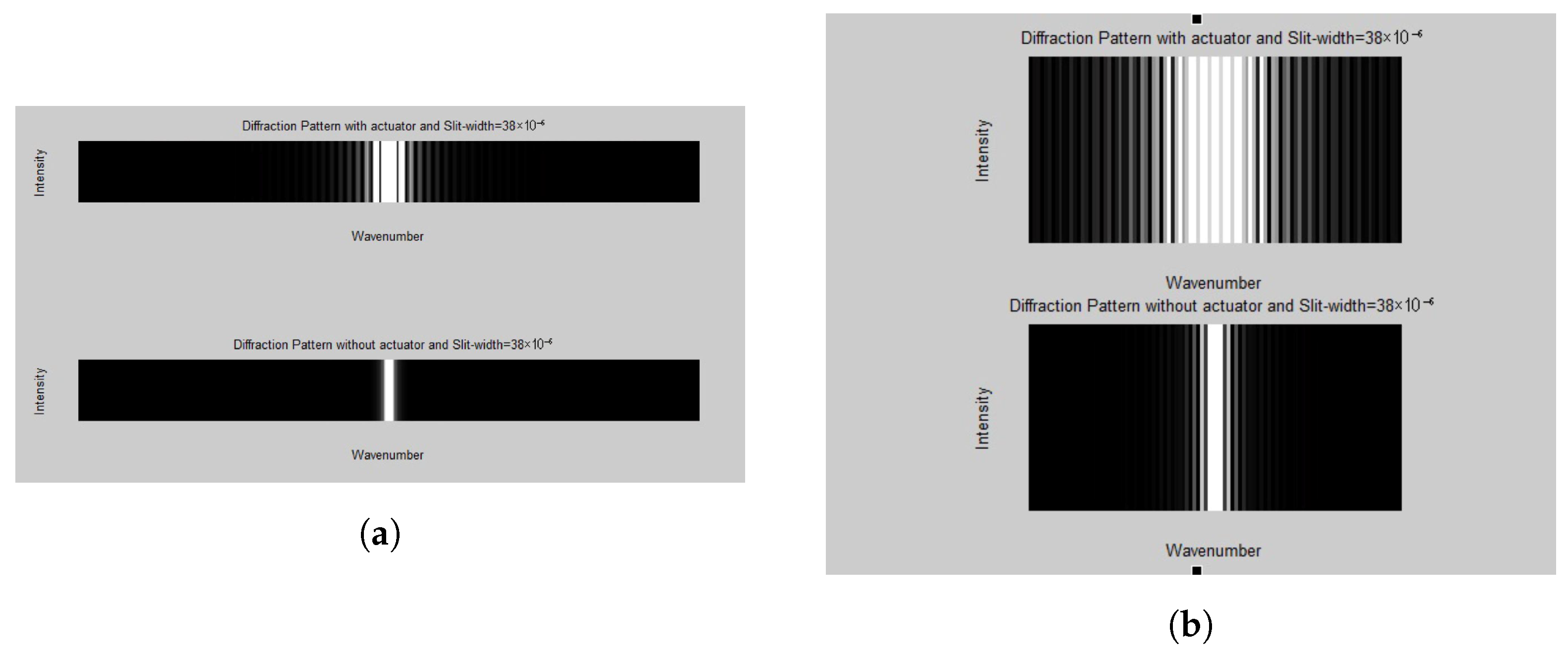
  • All the previous grating systems could automatically reach the level of resolution required, relying on the miniaturization of technology for that purpose. However, the current systems experience destructive interferences when the number of slits becomes large. This new system prevents that situation, allowing it to offer a better resolution.
Having assumed a perfect operation of the system above, we conduct a computer MATLAB investigation based on the analytical function dependence of parameters x , Δ , η , θ , D e in accordance with Figure 3, as follows.

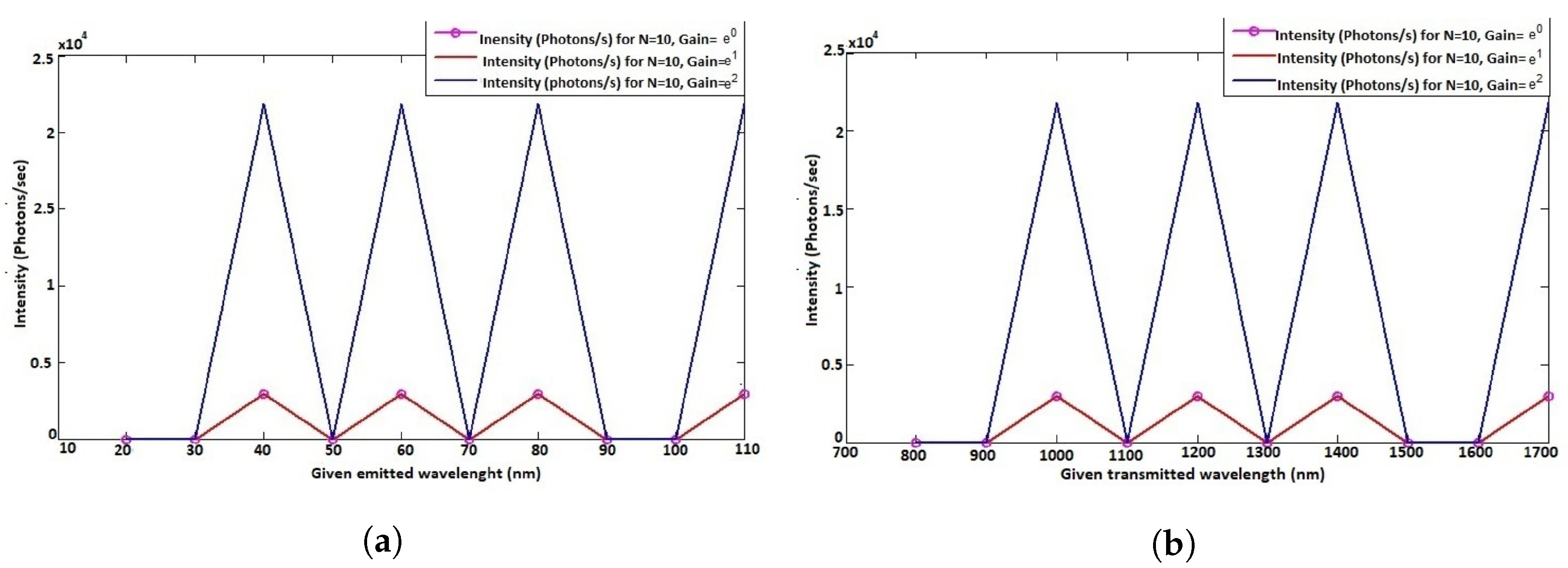
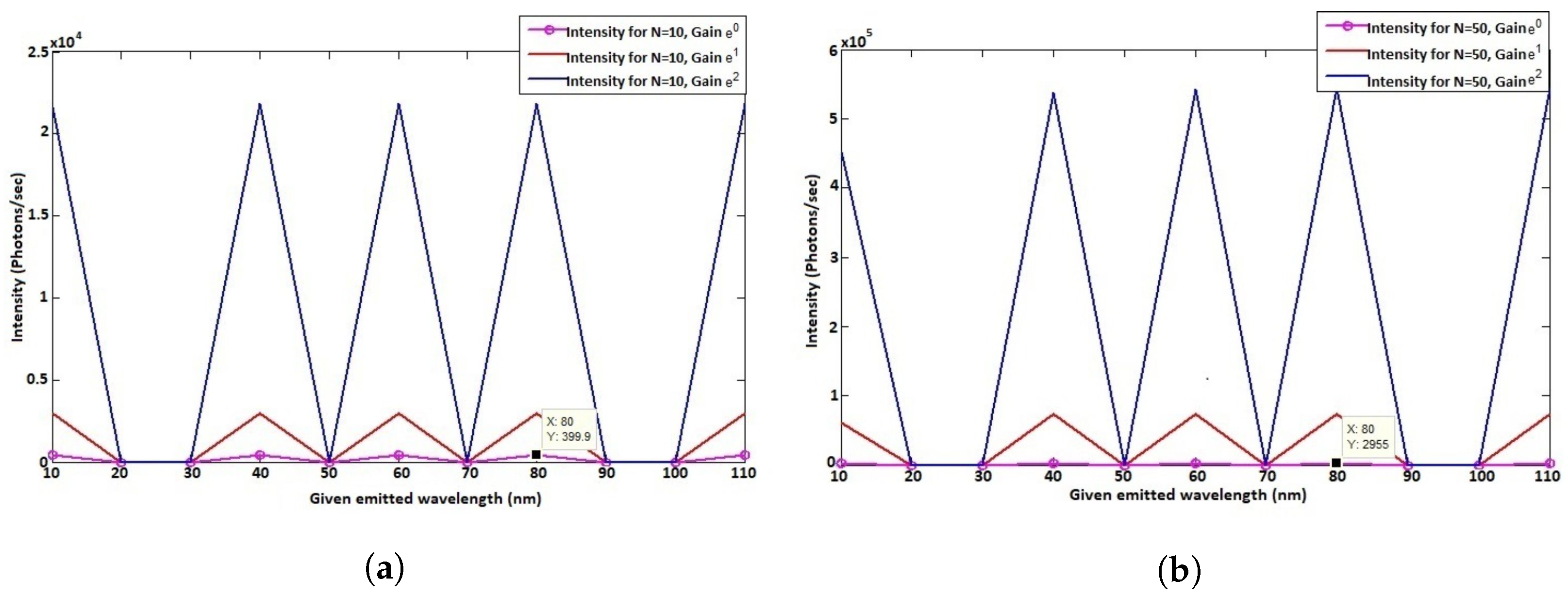
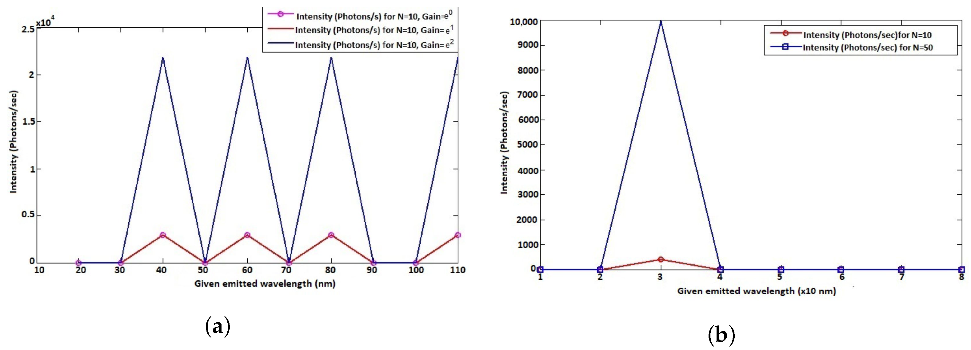
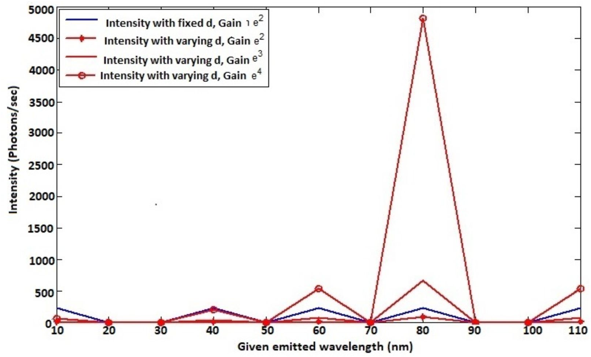
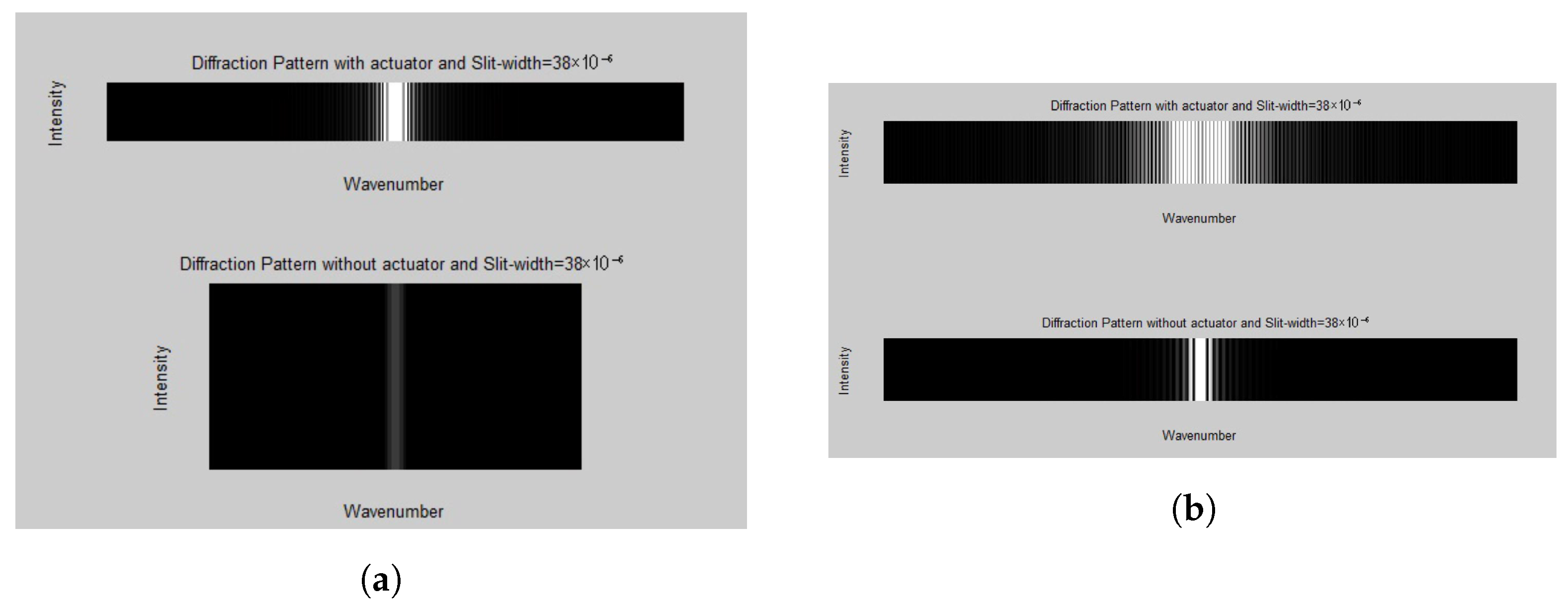
4.2. Analytical Results and Discussions

The investigation goes in accordance with the proposed system setup mentioned in Figure 5, made of parameters λ , x , Δ d , η , and D e . To exploit these parameters, we assume a sample emitting in a given range [20–110] nm from the microplastic retention particles, and transmitting light from a simple laser source emitting in a range [700–1700] nm. These emitted or transmitted wavelengths from a sample are detected by a sensor. We assume that on one side, the adapter associated with the LVDT sensor ensures the function f ( x , η ) , which is executed by a manipulable calibrator through its leveler l = f ( x , η , θ ) (Figure 3). Note that the gain η optimizes the intensity or flux of photons on the optimal display unit etendue and it is chosen to take on values η = 0 , 1 , 2 , for simplicity. On the other side, the MEMS associated with the LVDT sensor ensures that f ( Δ d , U ) applies f ( K , F ) to the actuator. We also assume that the display unit is likely capable of accommodating nanopixel CCD, as demonstrated in [19] and the current ongoing studies. It is under this description of parameters that we conduct our MATLAB investigation with the aim of verifying the impact of these parameters on the intensity, and on the image size, which is calculated using the diameter D e of the circle impacting the etendue.
For that purpose, we investigate the multi-level and simultaneity of wavelength processing capabilities of our system as well as its flexibility, using the overall function of the controller f ( η , Δ d , x θ ) . We take into account the fact that IR radiation may be absorbed by molecules and undergoes upconversion, producing smaller wavelengths, or downconversion, producing larger wavelengths during emission; that it may be transmitted after losing energy during collisions with molecules. Hence, the terms transmission and emission are used separately in this investigation.
We start investigating the effects of the adapter’s amplification of the signal. This is an anticipation on the possible attenuation, or perhaps, a lag of sufficient flux of photons that can be converted into electrons for a sufficient current on the display unit. The results of this investigation are given in Figure 12.
Figure 12 shows that, whether with emission (with or without Stokes or anti-Stokes shift) or with transmission (IR), a certain number of simultaneous wavelengths from a sample are displayed on the screen with the same bandwidth, exhibiting the multi-level functionality of the system. Furthermore, as expected in Figure 12, increasing η also increases the intensity, characteristic that is particularly important for brightness and accuracy on the display unit. This comes from the fact that increasing the number of photons per second means increasing the number of electrons converted as well, necessary in the display unit.
We also assess the influence of the number of slits N since it is likely to produce more dark fringes in theory when N becomes large, consequence of destructive interference. The results of this investigation are given in Figure 13.
In Figure 13, a quasi-similar observation of Figure 12 is seen when N increases, but with different objectives. As N increases, the radiation pattern will look just like a lone source signal, but more intense, clearer, and sharper due to bright fringe increase. N plays a crucial role in increasing image resolution, but not efficiency. This latter capability is the task of the adapter parameter x, which allows not only to increase the intensity, but also the system efficiency and accuracy by smoothing the spectra while avoiding the dark fringes on the system (see Figure 14).
Therefore, we proceed in investigating what could be the signal on the display unit with the existence and non-existence of our suggested system; the aim is to check its multi-wavelength capability compared with the classical solution, which is considered by letting x = 0 , η = 0 , Δ d = 0 . The results of this investigation are given in Figure 14.
We observe in Figure 14 the increased number of wavelengths diffracted successfully, with our proposed system (Figure 14a), proving the multi-level capability of our system, and confirming N’s role with the increase in bright fringes; which is not possible with the classical system (Figure 14b). Figure 12, Figure 13 and Figure 14 are very important as they tell us that when amplified, the increasing number of sources (slits) is well controlled, in accordance with the scale of the display unit. In normal classical circumstances, the system might simply experience destructive interference ( x = 0 in classical system) when N becomes large. However, the new system considers this abnormality with the provision of cos ( k x ) , which is controlled via the adapter by imposing to the calibrator a limit on x within specific intervals, for example [ lim Sup 0 , lim Inf λ 4 ] , which means 0 < | cos ( k x ) | < 1 , preventing the system from destructive interference when N becomes large.
Having observed the display side, we turn back to investigating the dynamism of the diffraction grating since our proposed solution also suggests a dynamic grating. We investigate how such a dynamism affects the system intensity, and these results are given in Figure 15.
Therefore, reducing the slit-width reduces the bandpass at the expense of the intensity, as shown in Figure 15. In our proposed system, when reducing the slit-width through Δ d , one observes, as expected, a reduction in the signal level; however, the system has provisions that mitigate the reduced intensity by amplifying it with the amplifier η value, as Figure 15 shows. However, what is important with Figure 15 is that as the wavelength increases, the system intensity increases as well. This comes with the fact that the diffraction angle decreases (not zero) when the wavelength increases, and that only the exact required slit-width or bandpass is presented to the incoming light, not too much bigger than the wavelength, in which case only a dot will appear on the display unit, and not too small because the diffracted light might go beyond the display unit. Consequently, if the adapter, through a proper calibrator x , concentrates the signal on the diameter of the etendue, then all the photon flux without loss reaches the etendue, as shown in Figure 15, keeping the clarity of the particle.
We further evaluate the different scenarios that determine the size of particles in a sample leaning on the absorbance and the diffraction angle, as well as the etendue and bandpass, all allowing for the characterization of the size of particles and accuracy. We choose the fixed mirror angle of π 33 while the diffraction angle varies within [ π 32 π 23 ] and the results are presented in Table 1.
To investigate the size based on the absorbance, we assumed that the IR source energy is absorbed by divers particles and the transmitted wavelengths are within [700–1000] nm. The results obtained are confined in Figure 16.
Figure 16 shows the effects of l = f ( x , η ) on particle size based on the absorbance and diffraction angle. The system exhibits blue or red shift (Figure 16a) and shows that the diffraction angle increases when the wavelength decreases (Figure 16b) in accordance with the size of particles. We all know that the diffraction angle increases when the slit-width decreases, hence the wavelength decrease observed. Figure 16, in sizing up particles compared to the wavelength, shows that there are red shift and blue shift possibilities with the absorbance spectrum, knowing that a right shift, known as red shift, detects particles of bigger size, or a left shift, known as blue shift, indicates smaller particles (Figure 16a). It is also shown in Figure 16b that the diffraction angle or diffraction pattern is bigger for smaller particles and vice versa.
To confirm this statement as well as the observed results on intensity and on image size, we carried on in evaluating the display unit’s etendue and image size, exploiting the x-dependent distance from the diffraction gratings to the display unit, and the emitted wavelength [50–200] nm of nanoparticles. These results are given in Table 1 for both cases: x = 0 , which is the classical solution, and x 0 , which is our proposed solution.
According to Table 1, the image size, or the space meant for the image is less than 10 nm when x 0 for nanoparticles in the range of vibration within [50–200] nm, while the minimum when x = 0 is 80 μ m , obliging the use of additional chemical for their detection. However, such a detection requires a nanopixel technology. Since the development of nanopixels is promising [19], it means that a nanopixel CCD that measures 10 × 10 in nanometer scale can be used to detect the content of the space meant for the image in the display unit, improving a micropixel CCD of 80 × 80 in micrometer scale when x = 0 , the classical condition. This is the necessary condition to detect particles of size less than 100 nm known as nanoplastics, or microplastics, particles of size less than 20 μ m , where 20 μ m has been, up to date, the limit size of IR detection of microplastics.
The observed increase in the number of bright fringes in the spectrum when N increases and x 0 is particularly important for detecting smallest-scale particles in imagery-based system. In fact, the adapter keeps unchanged a certain number of the classical characteristics such as the screen etendue as long as x = 0 . However, when x 0 , the defined etendue becomes the effective etendue embracing the signal size in accordance with its wavelength. This system flexibility is shown in Figure 15 and it is very important if we have to consider compressing or expanding the piezo-actuator that brings more flexibility in sizing up images.
As a result, we have improved the system efficiency, brightness, clarity, sharpness, accuracy, and ultimately, cost-effectiveness, with an increase in the system resolution, while preventing the system from destructive interference when N becomes large, or when the grating patterns vary, something the old system could not achieve. We have also achieved system multi-wavelength capability and system flexibility in accommodating the wavelength-dependent dynamism and in detecting different sizes of particles, as given in Table 1, results this paper intended to achieve. These results show more cost-effectiveness than the previous systems.
Having these results, as predicted by our theory, we carry on with their simulations to investigate how the screen will behave with different etendues and calibrator positions, and the system performance.

4.3. Simulations of the Results

We further conducted MATLAB simulations using the system setup above with the aim of confirming the results of our evaluations. For this purpose, we kept all the assumptions mentioned above, and we chose for the sake of this simulation a fixed display unit distance L = 1 m, and an initial uniform grating with slit-width W = 38 × 10 6 m, which is likely to change due to the associated MEMS actuator, in accordance with the function S = f ( λ , Δ d ) . In the current simulation, we assumed a slit-width reduction due to the actuator displacement and for the sake of simulation. Since we are interested in the IR spectrum, we would like to see how this spectrum behaves on the screen when varying the calibrator positions. Therefore, we assumed a laser source emitting a near-IR of 750 nm wavelength, and a sample emission or transmission within a range of [630–800] nm. To obtain this range, we assume that this wavelength may be absorbed and the molecule energy upconverted to yield VL emission [630–700] nm, or it may simply lose energy leading to a bigger wavelength [750–800] nm. The aim of this variation is to investigate the sensitivity of our system compared to the old one to several spectrum ranges for system integration capability, with the diffracted angle chosen to be 1 for numerical purposes. Since the theory requires that the calibrator moves at least within ( 0 λ 4 ) , we started checking the screen’s behavior from x = 200 mm, moving the numbers downward up to where an image appears for both our system and the old one. Henceforth, 50 mm was retained, and the other values were chosen in terms of the attainable objectives on the display units; that is, the required accuracy, sharpness, and brightness, without excluding the density of wavenumbers. Therefore, we retained the following calibrator positions [ 10 , 20 , 40 , 50 ] mm for the simulations. The display unit presents, for each case, our system and the old system for comparison purposes, or our system against the optimal position. In the end, we discuss the possible detectable size of particles or images. The results of these simulations are given in Figure 17, Figure 18 and Figure 19.
By carrying out MATLAB simulations of the proposed results, we realize that the system is flexible in accordance with our theory; the system is sensitive to all incoming wavelengths, which is not possible with the old system (Figure 17); the closer the display unit becomes, the clearer the image is on the display unit, as exhibited in Figure 18 and Figure 19. We also realize that all wavelengths not calibrated properly are not clear for our system, but almost non-existent on the display unit for the classical system, as Figure 17 shows, which depicts how sensitive our system is. To get further on a smaller scale, we manipulated the calibrator to find the proper caliber that allows us to observe the quasi-undetectable image. This is illustrated in Figure 18 and Figure 19. In these figures, one realized that each wavelength has its better calibrator position, as expected. For 750 nm, for instance, which corresponds approximately to 1.7 μ m etendue, 40 mm is the optimal position (Figure 18) for the calibrator, while it is 10 mm for 800 nm wavelength, which corresponds approximately to 1.8 μ m (Figure 19). In each case, when bringing closer the display unit using system Michelson, one realized that not only does the density of lines increase (Figure 18), but also, the lines initially not visible become detectable like in Figure 19b. It means that by adjusting the calibrator properly, smaller images that were previously invisible, as in Figure 18a and Figure 19a, become clearer, brighter, more intense, denser, and visible: hence, the possibility of smaller particle detection in Figure 18 and Figure 19b. High wavenumbers ( nm 1 ) are exhibited by the display unit of our system in Figure 18b and Figure 19b; as the theory indicates, bigger mass yields lower wavenumbers and vice versa, which shows that our display unit etendue is capable of detecting images up to the nanometer scale. This is confirmed by the numerical data provided in Table 1.

4.4. System Performance Analysis

In this performance analysis, we choose to evaluate the efficiency of the system and the signal-to-noise ratio, which are two important performance indicators. We have considered for that purpose that the environmental effects are negligible as well as any aberration.

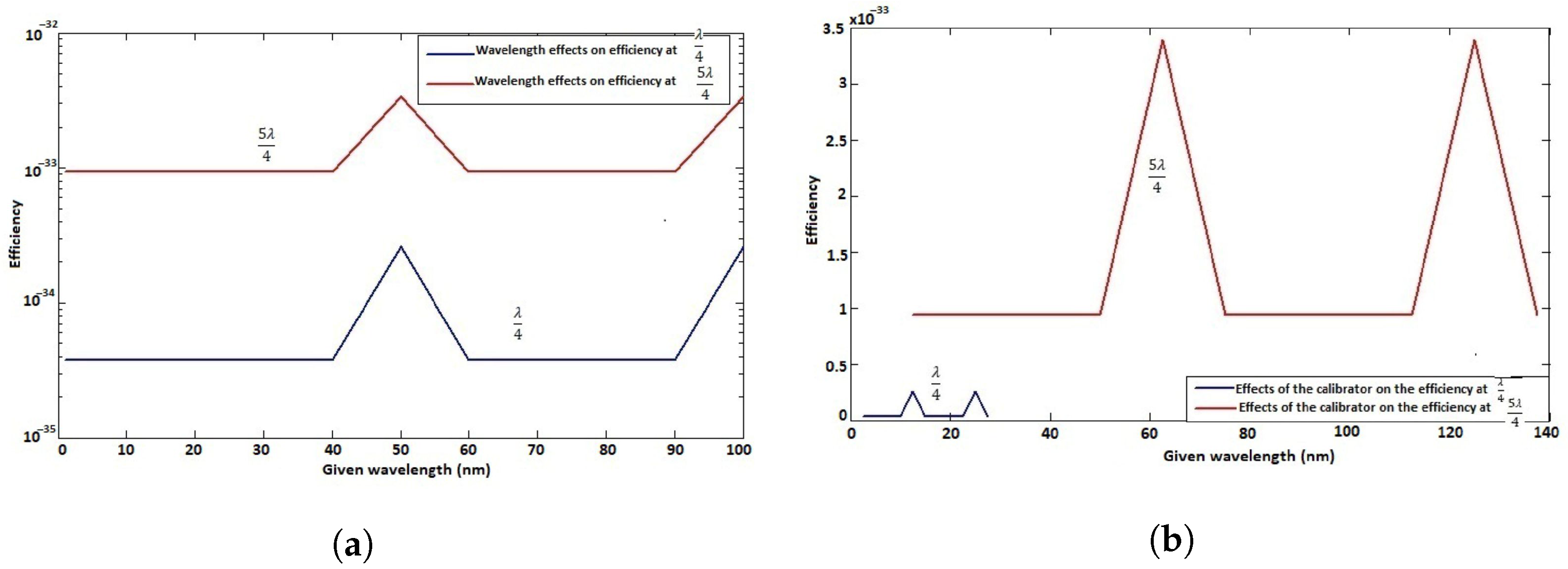
4.4.1. The System Efficiency

Let us consider a spectrophotometer made of a diffraction grating and a display unit containing a bandpass filter and a adapter magnifying the intensity, as in Figure 3. The slits being spaced d apart within a diffraction grating of total size a = N d , we can place the display unit at a distance L from the slits and height y = L tan θ .
Assuming θ is small, we can write y = L θ = L sin θ , and from Figure 3, sin θ = y L . The phase difference becomes, consequently, Δ ϕ = 2 π λ d y L .
The system efficiency is by definition, the ratio
E f = I p ( y ) I p ( 0 ) ,
which suggests that there is a possibility to express I p ( 0 ) in this ratio (28) when N becomes large (see Equation (13)). Assuming that the number of slits on the grating surface is large enough, that is, N , we can determine I p ( y ) from Equation (12) knowing that I p ( 0 ) = l i m y 0 I p ( y ) = I 0 N 2 , since x = 0 , η = 0 for y = 0 , bearing in mind that I p ( y ) can also be 1 4 normalized (since used as ratio), and that Δ ϕ 0 :
I P ( y ) = l i m N I p ( y ) = l i m N I 0 e 2 η cos ( k x ) sin ( N π d y 2 λ L ) sin ( π d y 2 λ L ) 2 = l i m N I p ( 0 ) e 2 η cos ( k x ) sin ( π a y 2 λ L ) π a y 2 λ L 2 = I p ( 0 ) e 2 η cos ( k x ) sin c ( a π y 2 λ L ) 2 ,
where we consider N d = a as the gratings range N .
From Equation (26), we can define the efficiency of the system as
E f = e 2 η cos ( k x ) sin c ( N π d y 2 λ L ) 2 .
The investigation on the system efficiency aims to show up to which level the image can be presented and magnified from the grating dynamism and the calibrator flexibility perspective. The results of this investigation are given in Figure 20.
According to the system efficiency results, the multi-level of the system is confirmed (Figure 20a) as well as the possibility of etendue reduction to accommodate smaller sizes of particle emission (Figure 20b).

4.4.2. Signal-to-Noise Ratio

To evaluate the signal-to-noise ratio, we made use of the ratio of intensity between the signal and the intensity of the stray light considered in this section as the only cause of light distortion. This consideration comes from the fact that we have neglected the factory impairments and environmental factors; the wavelength variations are managed by the controller, which prepares consequently the system for several diffraction patterns, and protects it from polarization effects, hysteresis, and creep. Sticking therefore only on the stray light, we determined the signal-to-noise ratio, which is defined here as the ratio S N R = I p I p n .
If it is important to determine the height y of the display unit, we cannot ignore the importance of determining the confinements of the image mapped on the screen, known as geometric etendue. For that purpose, L, θ , the incoming wavelength will play a crucial role as well as the distance between two slits, which is supposed to be uniformed and on which L depends. In that case, the normalized Equation (12) becomes
I p = I 0 e 2 η cos ( k x ) sin ( N π d λ sin θ ) 2 sin ( π d λ sin θ ) 2 .
In that option, we assume that the stray light is the only noise, defined as the random scattered signal, and can be expressed by considering θ as a random parameter θ n , and, perhaps, with a random phase with mean ϕ n . Assuming a uniform distribution of gratings, the probability that it falls within a collimated signal is 1 N . Therefore, the intensity when the stray light is considered in Equation (31) is given by
I p n = I 0 e 2 η N cos ( k x ) sin ( N π d λ sin θ n + ϕ n 2 ) 2 sin ( π d λ sin θ n + ϕ n 2 ) 2 .
Applying the ratio S N R = I p I p n , two cases are investigated, with and without pitch variation from the controller functions, and the results are in Figure 18. Note that the intensity I 0 is considered to be equal to 1 without loss of generality, and that we made use of the intensity graphs to evaluate the bandpass. The investigation conducted into the circumstance yielded results given in Figure 21.
When checking on how the stray light could affect the system in Figure 21, one notices that the signal with variable pitch (Figure 21b) is more affected by the random phases introduced by the stray light than the signal with fixed pitch (Figure 21a), which is normal: first, because the variation of the pitch increases the stray light, and second, because the reduction in the slit-width reduces the signal level, but the major cause is the composition of the stray light itself. As we know, stray light has the same composition as the radiated light [43], and in the absence or reduction in signal on an interval, stray light becomes dominant. However, we observe that the pitch variation shows robustness for the selected wavelengths, from the 800 nm wavelength, up to 1400 nm , which corresponds to a phase around 1.4–1.5 rad, where it is slightly affected, and an error which is such that 0.0032 I p < I p n < 0.00047 I p for 10 slits. At these points, the signal without pitch variation is wiped out as well as a mid lobe by the noise while our system shows some robustness through the depicted SNR. This comes from the fact that the detection system put in place is multi-bandwidth detection. After 1400 nm, there is almost no signal, hence the dominance of stray light as indicated, but with less intensity. However, by using its amplification provision, as [43] advised to, times the SNR by 10, to which we add a bandpass filter of B = 2 Δ λ H , with Δ λ H being the difference between the two half-points of the sinc intensity function, and assuming identical entry and exit slits, we can retrieve the required information from the sawtooth-like signal yielded by the stray light effects.
All these results obtained by varying the sample’s emission or transmission energy as well as the data collection and processing, allow our system to carry out Raman scattering; Raman spectroscopy and fluorescence; Photoluminescence; FTIR and IR spectroscopy; as well as Atomic Spectroscopy. This exhibits the potential integration of our system to the current existing techniques.

5. Conclusions

In this paper, through a control system, we adapted, in accordance with the wavelength, the geometry of a screen placed at a certain distance from the exit slits of the dynamic diffraction grating, preparing for the occasion of future universal spectroscopy/spectrophotometry. We did so by allowing almost all devices involved in the processing to operate without any direct wavelength dependence. We showed that with such a controller, having only the multi-wavelength sensor and the display unit being directly wavelength-dependent, we manage the system better by allocating the required slit-width or bandpass, etendue, and the magnification required to detect nano- and/or microplastics. We gave the characteristics and conditions for such a controller to switch from one scale to another. Based on those characteristics, we optimized the intensity, the position, as well as the screen etendue for brightness, sharpness, and accuracy, from where we derived the size of the image, as presented when combining spectroscopy and photometry. The resulting values of the geometric etendue of the screen and the image size are given, showing through simulation that it is possible to detect, among others, particles of size less than 14 nm , size-defining nanoplastics, and improving the IR microplastics that were limited to 20 μ m to lesser values. These obtained results show that our controller is in line with some characteristics known in the literature, such as the fact that it can exhibit blue or red shift from absorption emission, made use of to size up particles; it can amplify or attenuate the intensity or photon flux for accuracy and better resolution; it can filter the out-band signals, with the bandpass defined as B = 2 Δ λ ; make provision for the required etendue of the display unit; and most importantly, it can detect pathogens carried by microplastics for future pandemic prevention. The construction of such a spectrophotometer and the operability conditions of its sensors are left for further studies.

Author Contributions

Conceptualization, S.N., S.V.S., and J.M.; Methodology, S.N.; software, S.N.; validation, S.N.; formal analysis, S.N.; investigation, S.N.; resources, S.V.S. and J.M.; data curation, S.N.; writing original draft preparation, S.N.; writing review and editing, S.N.; visualization, S.N.; supervision, S.V.S., meyer; project administration, S.V.S. and J.M.; funding acquisition, S.V.S. All authors have read and agreed to the published version of the manuscript.

Funding

This research was funded by University of Johannesburg and The APC was funded by University of Johannesburg.

Data Availability Statement

Data will be made available as need raises.

Conflicts of Interest

The authors declare no conflicts of interest.

References

  1. Yu, K.I.; Yang, Y.; Wang, J.; Hartland, G.V.; Wang, G.P. Nanoparticle–Fluid Interactions at Ultrahigh Acoustic Vibration Frequencies Studied by Femtosecond Time-Resolved Microscopy. ACS Nano 2021, 15, 1833–1840. [Google Scholar] [CrossRef] [PubMed]
  2. Tian, N.; Zhou, Z.-Y.; Sun, S.-G.; Ding, Y.; Wang, Z.L. Synthesis of Tetrahexahedral Platinum Nanocrystals with High-Index Facets and High Electro-Oxidation Activity. Science 2007, 316, 732–735. [Google Scholar] [CrossRef] [PubMed]
  3. Dablemont, C.; Lang, P.; Mangeney, C.; Piquemal, J.Y.; Petkov, V.; Herbst, F.; Viau, G. FTIR and XPS synthesizes of Pt Nanoparticle Functionalization and Interaction with Alumina. Langmuir 2008, 24, 5832–5841. [Google Scholar] [CrossRef]
  4. Magdalini, V.; Charalampia, N.; Natasa, P.K.; Victoria, F.S. Analytical Methods for Nanomaterial Determination in Biological Matrices. Methods Protoc. 2022, 5, 61. [Google Scholar] [CrossRef] [PubMed] [PubMed Central]
  5. Wetzel, W. Advanced Raman Techniques for Micro- and Nanoplastics Detection. Spectroscopy Online. 2024. Available online: https://www.spectroscopyonline.com (accessed on 24 June 2025).
  6. Senturia, S.D.; Day, D.R.; Butler, M.A.; Smith, M.C. Programmable diffraction gratings and their uses in displays, spectroscopy, and communications. J. Microlithogr. Microfabr. Microsyst. 2005, 4, 041401. [Google Scholar]
  7. Schueller, O.J.A.; Duffy, D.C.; Rogers, J.A.; Brittain, S.T.; Whitesides, G.M. Reconfigurable diffraction gratings based on elastomeric microfluidic devices. Sens. Actuators A Phys. 1999, 78, 149–159. [Google Scholar] [CrossRef]
  8. Wong, C.W.; Jeon, Y.; Barbastathis, G.; Kim, S.G. Analog piezoelectric-driven tunable gratings with nanometer resolution. J. Microelectromech. Syst. 2004, 13, 998–1005. [Google Scholar] [CrossRef]
  9. Tormen, M.; Peter, Y.A.; Niedermann, P.A.; Hoogerwerf, S.H.; Stanley, R. Deformable MEMS grating for wide tunability and high operating speed. In Proceedings of the MOEMS-MEMS 2006 Micro and Nano-fabrication International Society for Optics and Photonics, Bellingham, WA, USA, 25 January 2006; p. 61140C. [Google Scholar]
  10. Yang, Y.S.; Lin, Y.H.; Hu, Y.C.; Liu, C.H. A large-displacement thermal actuator designed for MEMS pitch-tunable grating. J. Micromech. Microeng. 2008, 19, 015001. [Google Scholar] [CrossRef]
  11. Chorążewski, M.; Zajdel, P.; Feng, T.; Luo, D.; Lowe, A.R.; Brown, C.M.; Leão, J.B.; Li, M.; Bleuel, M.; Jensen, G.; et al. Compact Thermal Actuation by Water and Flexible Hydrophobic Nanopor. ACS Nano 2021, 15, 9048–9056. [Google Scholar] [CrossRef]
  12. Dadi, M.; Yasir, M. Spectroscopy and Spectrophotometry: Principles and Applications for Colorimetric and Related Other Analysis. In Colorimetry; Samanta, A.K., Ed.; InTechOpen: London, UK, 2022. [Google Scholar]
  13. Chen, C.; Chen, S.; Lobo, R.P.; Maciel-Escudero, C.; Lewin, M.; Taubner, T.; Xiong, W.; Xu, M.; Zhang, X.; Miao, X.; et al. Terahertz Nanoimaging and Nanospectroscopy of Chalcogenide Phase-Change Materials. ACS Photonics 2020, 7, 3499–3506. [Google Scholar] [CrossRef]
  14. Udvardi, B.; Kovács, I.J.; Fancsik, T.; Kónya, P.; Bátori, M.; Stercel, F.; Falus, G.; Szalai, Z. Effects of Particle Size on the Attenuated Total Reflection Spectrum of Minerals. Appl. Spectrosc. 2017, 71, 1157–1168. [Google Scholar] [CrossRef] [PubMed]
  15. Meyers, R.A. (Ed.) Encyclopedia of Physical Science and Technology, 3rd ed.; Academic Press Inc.: New York, NY, USA, 2003. [Google Scholar]
  16. Mille, D.A.B. Huygens’s wave propagation principle corrected. Opt. Lett. 1991, 16, 1370–1372. [Google Scholar] [CrossRef]
  17. Hecht, E. The Diffraction Grating. In Optics; Pearson: London, UK, 2017; Volume 497. [Google Scholar]
  18. Diffraction Grating Handbook, Lecture. Available online: https://citeseerx.ist.psu.edu/document?repid=rep1&type=pdf&doi=0953bdcdc08f1b5c1b9dfa199c2156030c3acce3 (accessed on 10 December 2024).
  19. Yunjie, W.; Haisong, J.; Kiichi, H. Space-mode compressor by using nano-pixel. Jpn. J. Appl. Phys. 2022, 61, SK1022. [Google Scholar] [CrossRef]
  20. Nanopixel: Promise Thin, Flexible, High-Res Displays. Oxford News 2014, University of Oxford, UK. Available online: https://www.ox.ac.uk/news (accessed on 10 December 2024).
  21. Nlend, S.; Sune, V.S.; Meyer, J. Characterization of a multilevel micro/nano-plastics Infrared Spectroscopy using optical chopper modulation and induced anti-stokes shift techniques. Results Opt. 2025, 18, 100775. [Google Scholar] [CrossRef]
  22. Zorabedian, P. Tunable external cavity semiconductor lasers. In Tunable Lasers Handbook; Duarte, F.J., Ed.; Elsevier: New York, NY, USA, 1995; Chapter 8. [Google Scholar]
  23. Ulrich, E.; Matthias, S.; Tim, P.C.; Jurgen, S. Novel Lasers: Short, shorter, shortest - Diode lasers in the deep ultraviolet Frequency-converted diode lasers provide continuous-wave light down to below 200 nm in the vacuum UV. Laser Focus World 2016, 52, 39–44. Available online: https://www.laserfocusworld.com/ (accessed on 5 May 2025).
  24. Gruber, G.; Neumayer, M.; Schweighofer Christian Doppler, B.; Leitner, T.; Berger, M.; Klösch, G. Linear Variable Differential Transformer in Harsh Environments—A Displacement and Thermal Study. In Proceedings of the 2023 IEEE International Instrumentation and Measurement Technology Conference (I2MTC), Kuala Lumpur, Malaysia, 13 July 2023. [Google Scholar]
  25. Haines, J.; Vitali, V.; Bottrill, K.; Naik, P.U.; Gandolfi, M.; De Angelis, C.; Franz, Y.; Lacava, C.; Petropoulos, P.; Guasoni, M. Fabrication of 1 × N integrated power splitters with arbitrary power ratio for single and multimode photonics. Nanophotonics 2024, 13, 339–348. [Google Scholar] [CrossRef]
  26. Sangjin, H.; Donggeun, R.; Junyung, P.; Hangsik, S. Design of Multiple Wavelength Optical Sensor Module for Depth-Dependent Photoplethysmography. Sensors 2019, 19, 5441. [Google Scholar] [CrossRef]
  27. Yong Joon, C.; Tsugumi, S.; Kakeru, N.; Mibu, R. Detection of Wavelength Information by Filter-Free Wavelength Sensor and Its Applications. ECS Trans. 2023, 112, 139–146. [Google Scholar]
  28. Yong-Joon, C.; Kakeru, N.; Tomoya, I.; Tsugumi, S.; Ryosuke, I.; Takeshi, H.; Daisuke, A.; Kazuhiro, T.; Toshihiko, N.; AndKazuaki, S. Demonstrating a Filter-Free Wavelength Sensor with Double-Well Structure and Its Application. Biosensors 2022, 12, 1033. [Google Scholar] [CrossRef]
  29. Li, C.Y.; Xiao, Y.T.; Fu, C.; Liang, F.X.; Chen, L.M.; Wu, D.; Luo, L.B. High-Accuracy and Broadband Wavelength Sensor with Detection Region Ranging from Deep Ultraviolet to Near Infrared Light. Adv. Optical Mater. 2021, 10, 2101735. [Google Scholar] [CrossRef]
  30. Jesus, U.; Salvador, H.; David, F.; Daniel, F.H. 3.3 kV PT-IGBT with voltage-sensor monolithically integrated channelled to the photogate by waveguide systems. IET Devices Circuits Syst. 2014, 8, 182–187. [Google Scholar] [CrossRef]
  31. Luna Innovations, LUNA-Data-Sheet-Micron-os7500. Available online: https://lunainc.com/ (accessed on 5 May 2025).
  32. Wilson, J.; Bergita, G.M.S.; Martina, P.; Mitra, D. Development of LVDT sensor as land displacement sensor. In Journal of Physics: Conference Series, Proceedings of the 4th International Seminar on Sensors, Instrumentation, Measurement and Metrology, Padang, Indonesia, 14 November 2019; IOP Publishing: Bristol, UK, 2019; Volume 1528. [Google Scholar]
  33. Monitran Sensors. Available online: https://www.monitran.com/ (accessed on 5 May 2025).
  34. Damgonovic, D. Material for High Temperature Piezoelectric Transducers Solid State. Mater. Sci. 1998, 3, 469. [Google Scholar]
  35. Wong, C.W.; Jeon, Y.; Barbastathis, G.; Kim, S.G. Analog tunable gratings driven by thin-film piezoelectric microelectromechanical actuators. Appl. Opt. 2003, 42, 621–626. [Google Scholar] [CrossRef]
  36. Guangcan, Z.; Zi, H.L.; Yi, Q.; Fook, S.C.; Guangya, Z. MEMS gratings and their applications. Int. J. Optomechatronics 2021, 15, 61–86. [Google Scholar] [CrossRef]
  37. Abdullah, S.A.; Mohd HMd, K.; John, O.D.; Abdelaziz, Y.A.; Sami, S.A.; Saeed SBa, H.; Mohammed, M.J. A Review of Actuation and Sensing Mechanisms in MEMS-Based Sensor Devices. Nanoscale Res Lett. 2021, 16, 16. [Google Scholar] [CrossRef] [PubMed] [PubMed Central]
  38. Nanxi, L.; Chong, P.H.; Shiyang, Z.; Yuan, H.F.; Yao, Z.; Lennon, Y.T.L. Aluminium nitride integrated photonics: A review. Nanophotonics 2021, 10, 2347–2387. [Google Scholar]
  39. Amalia, M.; Markos, P.; Nectarios, V.; Anastasios, P.; Georgios, E.S. Piezoelectric Actuators in Smart Engineering Structures Using Robust Control. Materials 2024, 17, 2357. [Google Scholar] [CrossRef]
  40. Thomas, E.S. Effect of Doping in Aluminium Nitride Nanomaterials: A review. Microsyst. Nanotechnol. 2021, 107, 15229. [Google Scholar] [CrossRef]
  41. Slide Switches. Available online: https://www.digikey.co.za/ (accessed on 3 May 2025).
  42. Scott, K.; Lacra, P.; Stewart Aitchison, J. Controlling a Semiconductor Optical Amplifier Using a State-Space Model. IEEE J. Quantum Electron. 2007, 43, 123–129. [Google Scholar] [CrossRef]
  43. Bradrick, T.D.; Churchich, J.E. Spectrophotometry and Spectrofluorimetry: A Practical Approach; Gore, M., Ed.; OUP Oxford: Oxford, UK, 2000; p. 225. [Google Scholar]
Figure 1. Diffraction grating principle.
Optics 06 00030 g001
Figure 2. Optical field evaluation.
Optics 06 00030 g002
Figure 3. Geometric definition of the display unit.
Optics 06 00030 g003
Figure 4. Reflection of the diffracted signal.
Optics 06 00030 g004
Figure 5. Controlled unit setup.
Optics 06 00030 g005
Figure 6. Multi-wavelength principle.
Optics 06 00030 g006
Figure 7. LVDT principle.
Optics 06 00030 g007
Figure 8. MEMS actuator principle: (a) rectilinear actuation, (b) bent beam actuation.
Optics 06 00030 g008
Figure 9. Adapter principle.
Optics 06 00030 g009
Figure 10. Calibrator deployment.
Optics 06 00030 g010
Figure 11. LUT of the controller.
Optics 06 00030 g011
Figure 12. (a) Effects of amplification on any given transmitted light intensity. (b) Effects of amplification on IR-transmitted light intensity.
Optics 06 00030 g012
Figure 13. (a) Effects of N on intensity for N = 10. (b) Effects of N on intensity for N = 50.
Optics 06 00030 g013
Figure 14. (a) Intensity with calibrator. (b) Intensity without calibrator.
Optics 06 00030 g014
Figure 15. Effects of pitch variation together with calibrator.
Optics 06 00030 g015
Figure 16. (a) Absorbance vs. wavelength: blue/red shift. (b) Diffraction angle vs. wavelength.
Optics 06 00030 g016
Figure 17. (a) Display unit for wavelength 630 nm and calibrator at 50 mm. (b) Display unit for wavelength 800 nm and calibrator at 50 mm.
Optics 06 00030 g017
Figure 18. (a) Display unit for wavelength 750 nm and calibrator at 50 mm. (b) Display unit for wavelength 750 nm and calibrator at 40 mm.
Optics 06 00030 g018
Figure 19. (a) Display unit for wavelength 800 nm and calibrator at 50 mm. (b) Display unit for wavelength 800 nm and calibrator at 10 mm.
Optics 06 00030 g019
Figure 20. (a) Wavelength effects on efficiency. (b) Calibrator effects on efficiency.
Optics 06 00030 g020
Figure 21. (a) Effects of stray light without pitch variation. (b) Effects of stray light with pitch variation.
Optics 06 00030 g021
Table 1. Nano/micro-geometry etendue and image size for emitted [50–200] nm wavelength.
ClassicalCalibratorAt x = 0
L = 2 L = 3 L = 4
Etendue50010001500 ( μ m 2 )
Image size80113138 ( μ m )
NewCalibratorat x 0 (New)
x = λ 4 x = 5 λ 4 x = 7 λ 4
Etendue0.1794.4768.772 ( nm 2 )
Image size0.4782.3873.342 (nm)
Disclaimer/Publisher’s Note: The statements, opinions and data contained in all publications are solely those of the individual author(s) and contributor(s) and not of MDPI and/or the editor(s). MDPI and/or the editor(s) disclaim responsibility for any injury to people or property resulting from any ideas, methods, instructions or products referred to in the content.

