Selective Transfer of Si Thin-Film Microchips by SiO2 Terraces on Host Chips for Fluidic Self-Assembly


Abstract
:
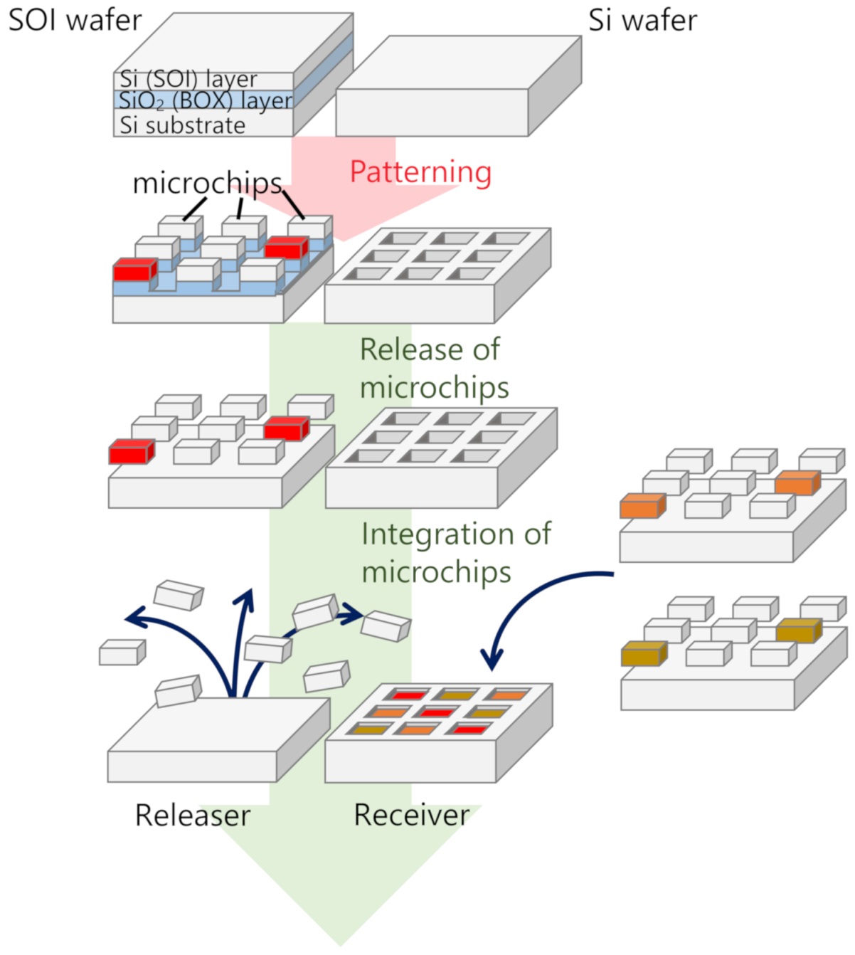
1. Introduction
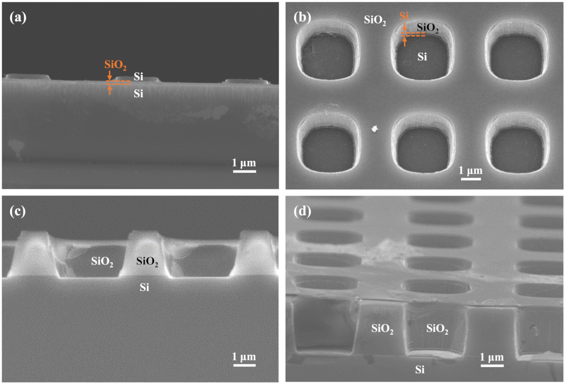
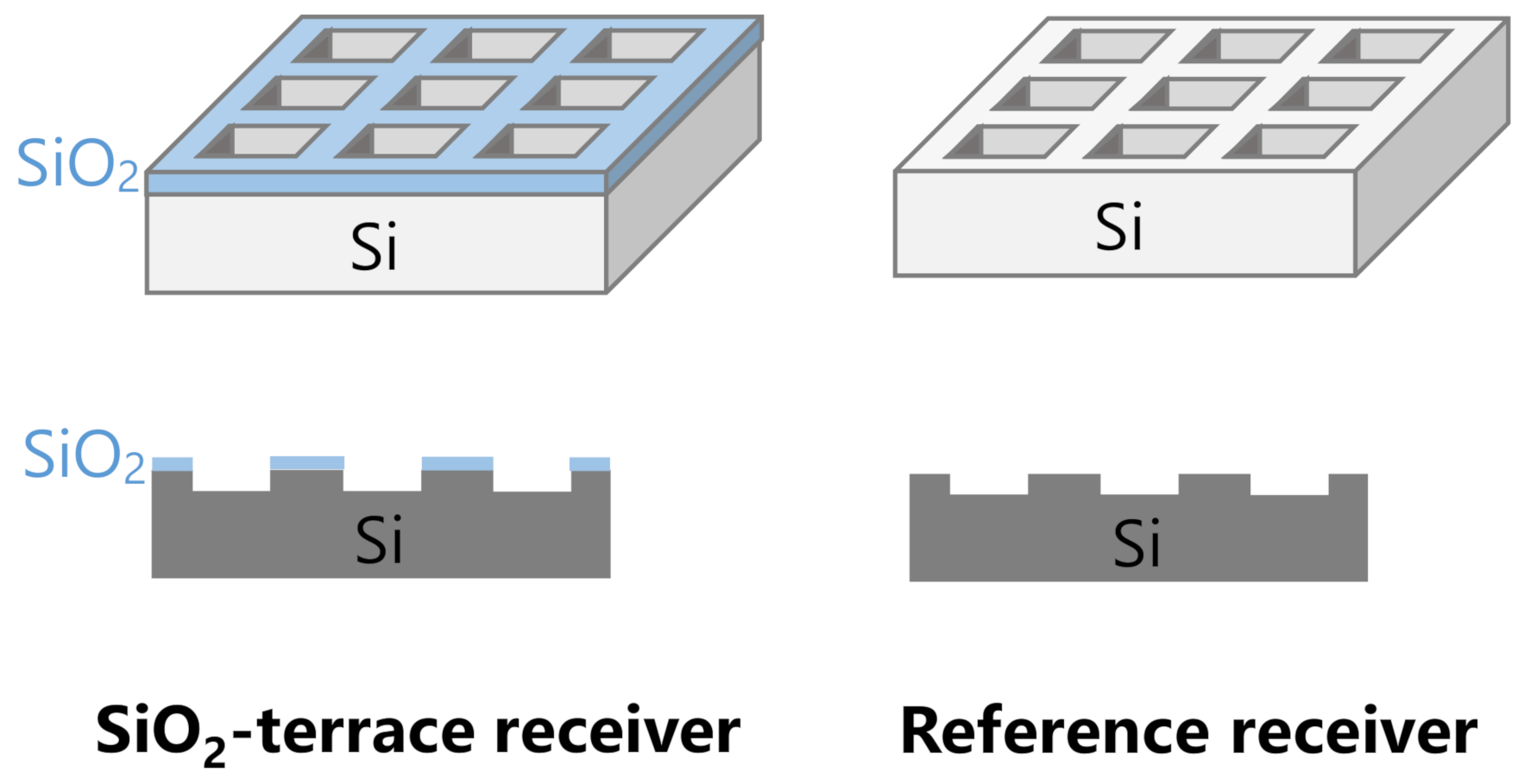
2. Materials and Methods
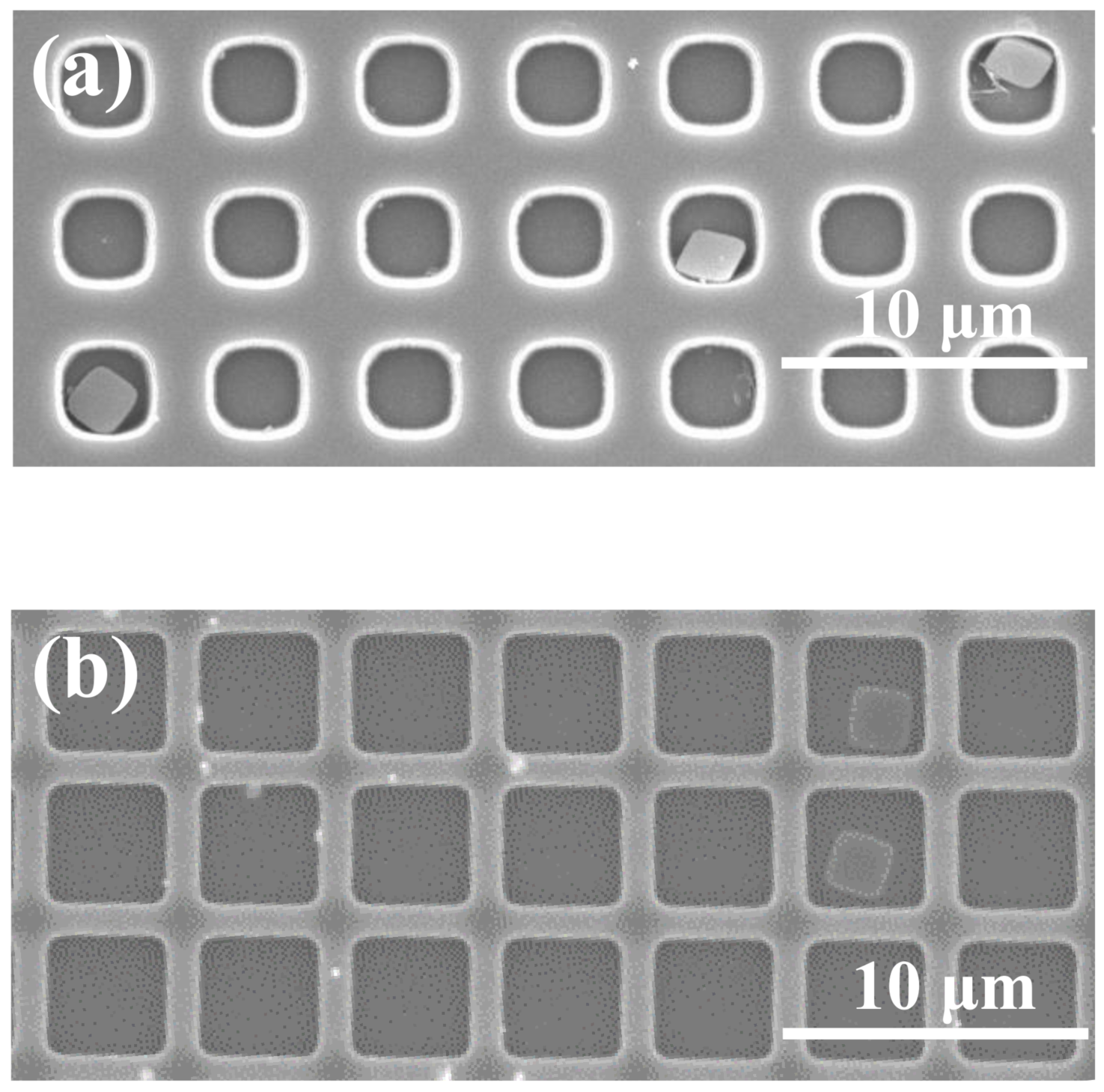
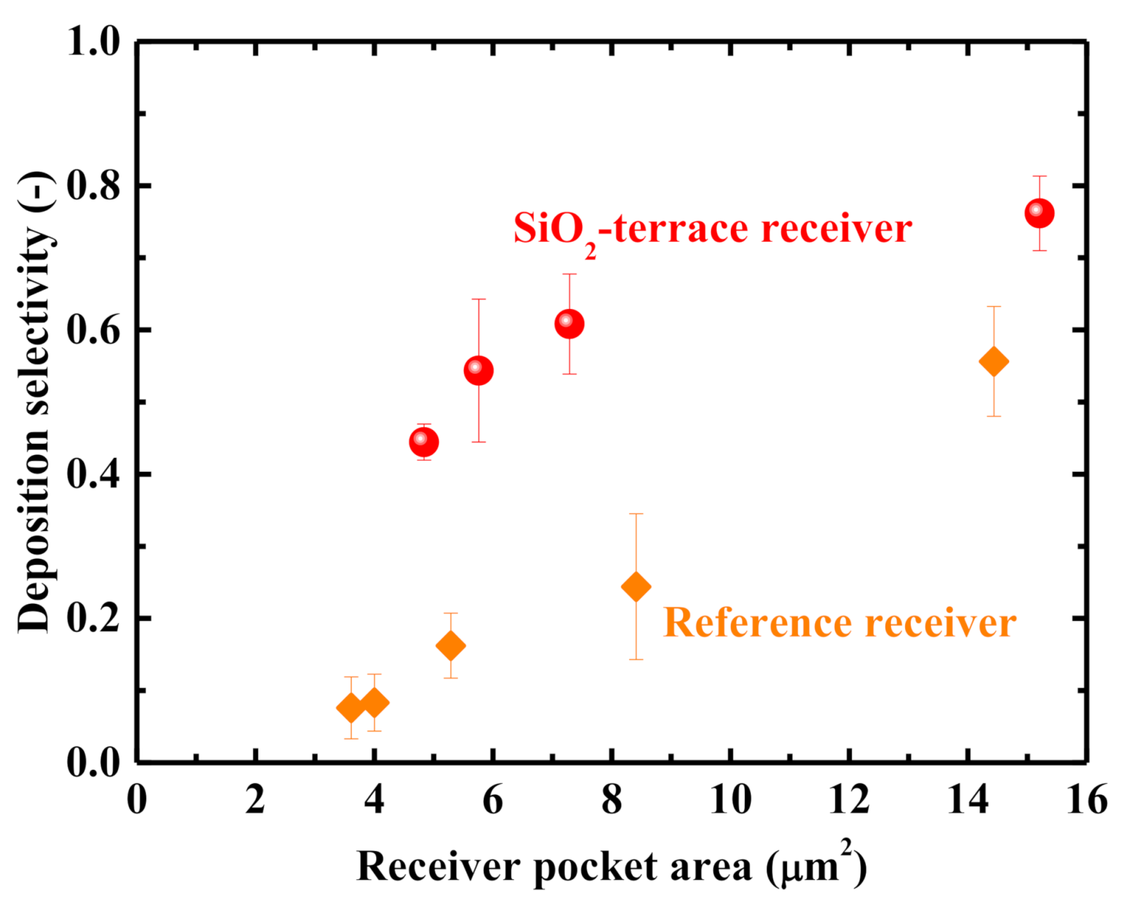
3. Results and Discussion
- (unit: force) for two spheres,
- (unit: force per area) for two flat surfaces facing each other, and
- (unit: force) for a sphere and a flat surface,
4. Conclusions
Author Contributions
Funding
Institutional Review Board Statement
Informed Consent Statement
Data Availability Statement
Acknowledgments
Conflicts of Interest
Appendix A

| Material 1 | Material 2 | Medium | A1 | A2 | Am | A |
|---|---|---|---|---|---|---|
| Si | Si | Water | 18.65 | 18.65 | 3.7 | 5.74 |
| Si | Si | Ethanol | 18.65 | 18.65 | 4.2 | 5.15 |
| Si | SiO2 | Water | 18.65 | 6.50 | 3.7 | 1.50 |
| Si | SiO2 | Ethanol | 18.65 | 6.50 | 4.2 | 1.13 |
| Si | Teflon | Water | 18.65 | 2.75 | 3.7 | −0.64 |
| Si | Teflon | Ethanol | 18.65 | 2.75 | 4.2 | −0.89 |
| Si | Si3N4 | Water | 18.65 | 16.70 | 3.7 | 5.18 |
| Si | Si3N4 | Ethanol | 18.65 | 16.70 | 4.2 | 4.62 |
| Si | HfO2 | Water | 18.65 | 5.63 | 3.7 | 1.08 |
| Si | HfO2 | Ethanol | 18.65 | 5.63 | 4.2 | 0.73 |
| Si | ZrO2 | Water | 18.65 | 20 | 3.7 | 6.10 |
| Si | ZrO2 | Ethanol | 18.65 | 20 | 4.2 | 5.50 |
| Si | Silsesquioxanes | Water | 18.65 | 5.5 | 3.7 | 1.01 |
| Si | Silsesquioxanes | Ethanol | 18.65 | 5.5 | 4.2 | 0.67 |
| Si | Allyl ethers | Water | 18.65 | 4.5 | 3.7 | 0.47 |
| Si | Allyl ethers | Ethanol | 18.65 | 4.5 | 4.2 | 0.16 |
References
- Banerjee, K.; Souri, S.J.; Kapur, P.; Saraswat, K.C. 3-D ICs: A novel chip design for improving deep-submicrometer interconnect performance and systems-on-chip integration. Proc. IEEE 2001, 89, 602–633. [Google Scholar] [CrossRef] [Green Version]
- Sun, C.; Wade, M.T.; Lee, Y.; Orcutt, J.S.; Alloatti, L.; Georgas, M.S.; Waterman, A.S.; Shainline, J.M.; Avizienis, R.R.; Lin, S.; et al. Single-chip microprocessor that communicates directly using light. Nature 2015, 528, 534–538. [Google Scholar] [CrossRef] [PubMed] [Green Version]
- Itoh, K.; Kuno, Y.; Hayashi, Y.; Suzuki, J.; Hojo, N.; Amemiya, T.; Nishiyama, N.; Arai, S. Crystalline/amorphous Si integrated optical couplers for 2D/3D interconnection. IEEE J. Select Top. Quant. Electron. 2016, 22, 255–263. [Google Scholar] [CrossRef] [Green Version]
- Shulaker, M.M.; Hills, G.; Park, R.S.; Howe, R.T.; Saraswat, K.; Wong, H.S.P.; Mitra, S. Three-dimensional integration of nanotechnologies for computing and data storage on a single chip. Nature 2017, 547, 74–78. [Google Scholar] [CrossRef]
- Yamauchi, Y.; Okano, M.; Shishido, H.; Noda, S.; Takahashi, Y. Implementing Raman silicon nanocavity laser for integrated optical circuits by using a (100) SOI wafer with a 45-degree-rotated top silicon layer. OSA Contin. 2019, 2, 2098–2112. [Google Scholar] [CrossRef]
- Geum, D.-M.; Kim, S.-K.; Kang, C.-M.; Moon, S.-H.; Kyhm, J.; Han, J.-H.; Lee, D.-S.; Kim, S.-H. Strategy toward the fabrication of ultrahigh-resolution micro-LED displays by bonding interface-engineered vertical stacking and surface passivation. Nanoscale 2019, 11, 23139–23148. [Google Scholar] [CrossRef] [PubMed]
- Atsumi, Y.; Watabe, K.; Uda, N.; Miura, N.; Sakakibara, Y. Initial alignment control technique using on-chip groove arrays for liquid crystal hybrid silicon optical phase shifters. Opt. Express 2019, 27, 8756–8767. [Google Scholar] [CrossRef] [PubMed]
- Yeh, H.J.; Smith, J.S. Fluidic self-assembly for the integration of GaAs light-emitting diodes on Si substrate. IEEE Photon. Technol. Lett. 1994, 6, 706–708. [Google Scholar] [CrossRef]
- Tu, J.K.; Talghader, J.J.; Hadley, M.A.; Smith, J.S. Fluidic self-assembly of InGaAs vertical cavity surface emitting lasers onto silicon. Electron. Lett. 1995, 31, 1448–1449. [Google Scholar] [CrossRef]
- Talghader, J.J.; Tu, J.K.; Smith, J.S. Integration of fluidically self-assembled optoelectronic devices using a silicon-based process. IEEE Photon. Technol. Lett. 1995, 7, 1321–1323. [Google Scholar] [CrossRef]
- Edman, C.F.; Swint, R.B.; Gurtner, C.; Formosa, R.E.; Roh, S.D.; Lee, K.E.; Swanson, P.D.; Ackley, D.E.; Coleman, J.J.; Heller, M.J. Electric field directed assembly of an InGaAs LED onto silicon circuitry. IEEE Photon. Technol. Lett. 2000, 12, 1198–1200. [Google Scholar] [CrossRef]
- Jacobs, H.O.; Tao, A.R.; Schwartz, A.; Gracias, D.H.; Whitesides, G.M. Fabrication of a cylindrical display by patterned assembly. Science 2002, 296, 323–325. [Google Scholar] [CrossRef] [PubMed] [Green Version]
- Chung, S.E.; Park, W.; Shin, S.; Lee, S.A.; Kwon, S. Guided and fluidic self-assembly of microstructures using railed microfluidic channels. Nat. Mater. 2008, 7, 581–587. [Google Scholar] [CrossRef] [PubMed]
- Park, S.-C.; Fang, J.; Biswas, S.; Mozafari, M.; Stauden, T.; Jacobs, H.O. A first implementation of an automated reel-to-reel fluidic self-assembly machine. Adv. Mater. 2014, 26, 5942–5949. [Google Scholar] [CrossRef] [PubMed] [Green Version]
- Kaltwasser, M.; Schmidt, U.; Biswas, S.; Reiprich, J.; Schlag, L.; Angel Isaac, N.; Stauden, T.; Jacobs, H.O. Core-shell transformation-imprinted solder bumps enabling low-temperature fluidic self-assembly and self-alignment of chips and high melting point interconnects. ACS Appl. Mater. Interfaces 2018, 10, 40608–40613. [Google Scholar] [CrossRef] [PubMed]
- Ishihara, S.; Tanabe, K. Nanoscale silicon fluidic transfer for ultrahigh-density self-assembled integration. Nano Express 2020, 1, 010063. [Google Scholar] [CrossRef]
- Love, J.C.; Urbach, A.R.; Prentiss, M.G.; Whitesides, G.M. Three-dimensional self-assembly of metallic rods with submicron diameters using magnetic interactions. J. Am. Chem. Soc. 2003, 125, 12696–12697. [Google Scholar] [CrossRef]
- Gao, J.H.; Zhang, B.; Zhang, X.X.; Xu, B. Magnetic-dipolar-interaction-induced self-assembly affords wires of hollow nanocrystals of cobalt selenide. Angew. Chem. Int. Ed. 2006, 45, 1220–1223. [Google Scholar] [CrossRef] [PubMed]
- Tong, Q.-Y.; Goesele, U. Semiconductor Wafer Bonding: Science and Technology, 1st ed.; Wiley: New York, NY, USA, 1999; pp. 17–24. [Google Scholar]
- Leite, F.L.; Bueno, C.C.; Da Róz, A.L.; Ziemath, E.C.; Oliveira, O.N., Jr. Theoretical models for surface forces and adhesion and their measurement using atomic force microscopy. Int. J. Mol. Sci. 2012, 13, 12773–12856. [Google Scholar] [CrossRef]
- Bergstrom, L.; Meurk, A.; Arwin, H.; Rowcliffe, D.J. Estimation of Hamaker constants of ceramic materials from optical data using Lifshitz theory. J. Am. Ceram. Soc. 1996, 79, 339–348. [Google Scholar] [CrossRef]
- Eastman, J. Stability of charge-stabilised colloids. In Colloid Science: Principles, Methods and Applications, 2nd ed.; Cosgrove, T., Ed.; Wiley: West Sussex, UK, 2010; p. 47. [Google Scholar]
- Israelachvili, J.N. Intermolecular and Surface Forces, 3rd ed.; Academic Press: Burlington, MA, USA, 2011; p. 263. [Google Scholar]
- Eom, N.; Parsons, D.F.; Craig, V.S.J. Measurement of long range attractive forces between hydrophobic surfaces produced by vapor phase adsorption of palmitic acid. Soft Matter 2017, 13, 8910–8921. [Google Scholar] [CrossRef] [PubMed]
- Takagishi, H.; Masuda, T.; Shimoda, T.; Maezono, R.; Hongo, K. Method for the calculation of the Hamaker constants of organic materials by the Lifshitz macroscopic approach with density functional theory. J. Phys. Chem. A 2019, 123, 8726–8733. [Google Scholar] [CrossRef] [PubMed] [Green Version]

Publisher’s Note: MDPI stays neutral with regard to jurisdictional claims in published maps and institutional affiliations. |
© 2021 by the authors. Licensee MDPI, Basel, Switzerland. This article is an open access article distributed under the terms and conditions of the Creative Commons Attribution (CC BY) license (http://creativecommons.org/licenses/by/4.0/).
Share and Cite
Fujita, Y.; Ishihara, S.; Nakashima, Y.; Nishigaya, K.; Tanabe, K. Selective Transfer of Si Thin-Film Microchips by SiO2 Terraces on Host Chips for Fluidic Self-Assembly. Appl. Mech. 2021, 2, 16-24. https://doi.org/10.3390/applmech2010002
Fujita Y, Ishihara S, Nakashima Y, Nishigaya K, Tanabe K. Selective Transfer of Si Thin-Film Microchips by SiO2 Terraces on Host Chips for Fluidic Self-Assembly. Applied Mechanics. 2021; 2(1):16-24. https://doi.org/10.3390/applmech2010002
Chicago/Turabian StyleFujita, Yutaka, Shoji Ishihara, Yuki Nakashima, Kosuke Nishigaya, and Katsuaki Tanabe. 2021. "Selective Transfer of Si Thin-Film Microchips by SiO2 Terraces on Host Chips for Fluidic Self-Assembly" Applied Mechanics 2, no. 1: 16-24. https://doi.org/10.3390/applmech2010002
APA StyleFujita, Y., Ishihara, S., Nakashima, Y., Nishigaya, K., & Tanabe, K. (2021). Selective Transfer of Si Thin-Film Microchips by SiO2 Terraces on Host Chips for Fluidic Self-Assembly. Applied Mechanics, 2(1), 16-24. https://doi.org/10.3390/applmech2010002