GERARD: GEneral RApid Resolution of Digital Mazes Using a Memristor Emulator

 ,
,  ,
,  and
and 
Abstract
:1. Introduction
2. General Method
- It stops listening to any other input, so no other signal can trigger it.
- It identifies and stores the triggering input port.
- It propagates the signal to all its non-activated ports.
3. Algorithm Implementation
3.1. Memristor Model Implementation
3.2. MATLAB Implementation
- Program all memristors with a memristance value M corresponding to the distance between nodes.
- Set the starting point, taking into account that the bottom right element is the end by default (without any loss of generality).
- Start counting with the first node and propagate the signal to its neighbors with a delay given by Equation (2).
- When a node receives an input signal, it is marked as active and treated as a new starting point.
- Repeat from step no. 3 until the final node is reached.
- If the end node is reached, a signal that the process is finished is sent to the control unit, and the shortest path is then retrieved.
3.3. Programmable Device Implementation
3.3.1. Communications Block
3.3.2. Interconnection Block
3.3.3. Node Element
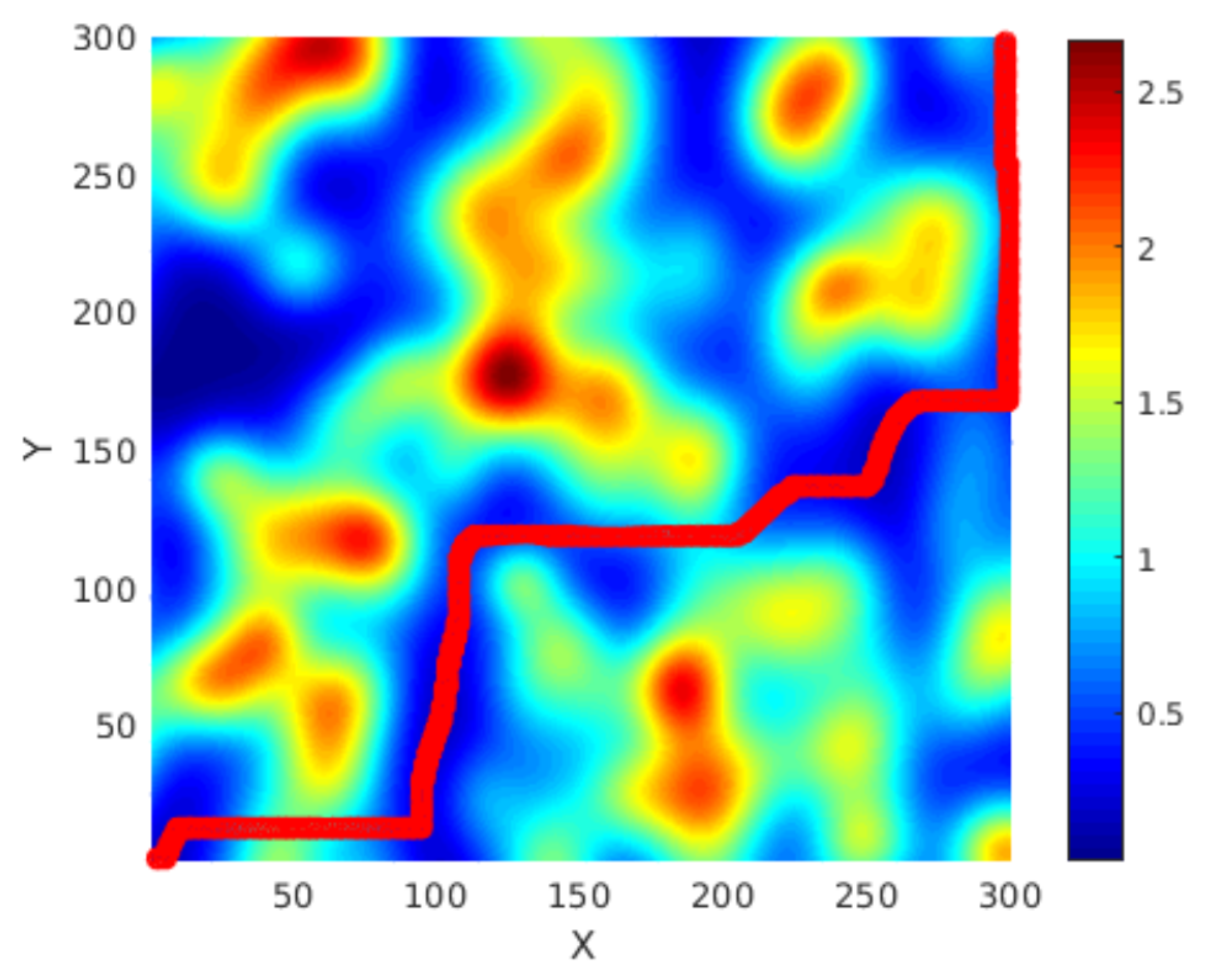
4. Results
5. Conclusions
Author Contributions
Funding
Data Availability Statement
Conflicts of Interest
References
- Mishra, S.; Bande, P. Maze solving algorithms for micro mouse. In Proceedings of the 4th International Conference on Signal Image Technology and Internet Based Systems (SITIS 2008), Bali, Indonesia, 30 November–3 December 2008; Dipanda, A., Chbeir, R., Yetongnon, K., Eds.; IEEE, Inc.: Danvers, MA, USA, 2008; pp. 86–93. [Google Scholar] [CrossRef]
- Fattah, M.; Airola, A.; Ausavarungnirun, R.; Mirzaei, N.; Liljeberg, P.; Plosila, J.; Mohammadi, S.; Pahikkala, T.; Mutlu, O.; Tenhunen, H. A low-overhead, fully-distributed, guaranteed-delivery routing algorithm for faulty network-on-chips. In Proceedings of the 2015 IEEE/ACM Ninth International Symposium on Networks-on-Chip (NOCS’15), Vancouver, BC, Canada, 28–30 September 2015; Ivanov, A., Marculescu, D., Pratim Pande, P., Flich, J., Eds.; Association for Computing Machinery: New York, NY, USA, 2015. [Google Scholar] [CrossRef]
- Kathe, O.; Turkar, V.; Jagtap, A.; Gidaye, G. Maze solving robot using image processing. In Proceedings of the 2015 IEEE Bombay Section Symposium (IBSS), Mumbai, India, 10–11 September 2015; Banerjee, A., Lobo, A., Satyanarayana, B., Doolla, S., Eds.; IEEE: Danvers, MA, USA, 2015. [Google Scholar] [CrossRef]
- Suriyanath. Dijkstra Algorithm. Available online: https://www.mathworks.com/matlabcentral/fileexchange/46883-dijkstra-algorithm (accessed on 15 December 2021).
- Caruso, F.; Crespi, A.; Ciriolo, A.G.; Sciarrino, F.; Osellame, R. Fast escape of a quantum walker from an integrated photonic maze. Nat. Commun. 2016, 7, 11682. [Google Scholar] [CrossRef]
- Vourkas, I.; Stathis, D.; Sirakoulis, G.C. Massively parallel analog computing: Ariadne’s thread was made of memristors. IEEE Trans. Emerg. Top. Comput. 2015, 6, 145–155. [Google Scholar] [CrossRef]
- Papandroulidakis, G.; Vourkas, I.; Sirakoulis, G.C.; Stavrinides, S.G.; Nikolaidis, S. Multi-state memristive nanocrossbar for high-radix computer arithmetic systems. In Proceedings of the 2015 IEEE 15th International Conference on Nanotechnology (IEEE NANO 2015), Rome, Italy, 27–30 July 2015; Di Carlo, A., Sarto, M.S., Lugli, P., Eds.; IEEE: Danvers, MA, USA, 2015; pp. 625–628. [Google Scholar] [CrossRef]
- Pershin, Y.V.; Di Ventra, M. Solving mazes with memristors: A massively parallel approach. Phys. Rev. E 2011, 84, 046703. [Google Scholar] [CrossRef] [PubMed] [Green Version]
- Chua, L. Memristor—The missing circuit element. IEEE Trans. Circuit Theory 1971, 18, 507–519. [Google Scholar] [CrossRef]
- Chua, L. Resistance switching memories are memristors. Appl. Phys. A 2011, 102, 765–783. [Google Scholar] [CrossRef] [Green Version]
- Biolek, D.; Kolka, Z.; Biolková, V.; Biolek, Z.; Potrebić, M.; Tošić, D. Modeling and simulation of large memristive networks. Intl. J. Circuit Theory Appl. 2018, 46, 50–65. [Google Scholar] [CrossRef]
- Batas, D.; Fiedler, H. A memristor SPICE implementation and a new approach for magnetic flux-controlled memristor modeling. IEEE Trans. Nanotechnol. 2010, 10, 250–255. [Google Scholar] [CrossRef]
- Biolek, Z.; Biolek, D.; Biolkova, V. SPICE model of memristor with nonlinear dopant drift. Radioengineering 2009, 18, 210–214. Available online: https://www.radioeng.cz/fulltexts/2009/09_02_210_214.pdf (accessed on 15 December 2021).
- Mladenov, V. A unified and open LTSPICE memristor model library. Electronics 2021, 10, 1594. [Google Scholar] [CrossRef]
- Garcia-Moreno, E.; Picos, R.; Al-Chawa, M.M. SPICE model for unipolar RRAM based on a flux-controlled memristor. In Proceedings of the 2015 IEEE International Autumn Meeting on Power, Electronics and Computing (ROPEC), Ixtapa, Mexico, 4–6 November 2015; Cerda Jacobo, J., Ed.; IEEE, Inc.: Danvers, MA, USA, 2015. [Google Scholar] [CrossRef]
- Garcia-Redondo, F.; Gowers, R.P.; Crespo-Yepes, A.; López-Vallejo, M.; Jiang, L. SPICE compact modeling of bipolar/unipolar memristor switching governed by electrical thresholds. IEEE Trans. Circuits Syst. I Regul. Pap. 2016, 63, 1255–1264. [Google Scholar] [CrossRef] [Green Version]
- Svetoslavov, G.; Camps, O.; Stavrinides, S.G.; Picos, R. A Switched capacitor memristive emulator. IEEE Trans. Circuits Syst. II Express Briefs 2020, 68, 1463–1466. [Google Scholar] [CrossRef]
- Camps, O.; Stavrinides, S.G.; Picos, R. Efficient implementation of memristor cellular nonlinear networks using stochastic computing. In Proceedings of the 24th European Conference on Circuit Theory and Design (ECCTD 2020), Sofia, Bulgaria, 7–10 September 2020; Slavova, A., Tetzlaf, R., Eds.; IEEE: Danvers, MA, USA, 2020. [Google Scholar] [CrossRef]
- Saxena, V. A Compact CMOS memristor emulator circuit and its applications. In Proceedings of the 2018 IEEE 61st International Midwest Symposium on Circuits and Systems (MWSCAS), Windsor, ON, Canada, 5–8 August 2018; Bayoumi, M., Ahmadi, M., Eds.; IEEE: Danvers, MA, USA, 2018; pp. 190–193. [Google Scholar] [CrossRef] [Green Version]
- Yu, D.S.; Sun, T.T.; Zheng, C.Y.; Iu, H.; Fernando, T. A simpler memristor emulator based on varactor diode. Chin. Phys. Lett. 2018, 35, 058401. [Google Scholar] [CrossRef]
- Pershin, Y.V.; Di Ventra, M. Emulation of floating memcapacitors and meminductors using current conveyors. Electron. Lett. 2011, 47, 243–244. [Google Scholar] [CrossRef] [Green Version]
- Vourkas, I.; Abusleme, A.; Ntinas, V.; Sirakoulis, G.C.; Rubio, A. A digital memristor emulator for FPGA-based artificial neural networks. In Proceedings of the 1st International Verification and Security Workshop (IVSW), Sant Feliu de Guixols, Spain, 4–6 July 2016; IEEE: Danvers, MA, USA, 2016. [Google Scholar] [CrossRef]
- Volos, C.; Pham, V.-T. (Eds.) Mem-Elements for Neuromorphic Circuits with Artificial Intelligence Applications; Academic Press: San Diego, CA, USA, 2021. [Google Scholar]
- Wang, N.; Zhang, G.; Bao, H. Bursting oscillations and coexisting attractors in a simple memristor-capacitor-based chaotic circuit. Nonlinear Dyn. 2019, 97, 1477–1494. [Google Scholar] [CrossRef]
- Picos, R.; Roldan, J.; Al Chawa, M.; Jimenez-Molinos, F.; Garcia-Moreno, E. A physically based circuit model to account for variability in memristors with resistive switching operation. In Proceedings of the 2016 Conference on Design of Circuits and Integrated Systems (DCIS 2016), Granada, Spain, 23–25 November 2016; Parrilla, L., López-Villanueva, J.A., Santos, M., Garcìa, A., Eds.; IEEE: Danvers, MA, USA, 2016. [Google Scholar] [CrossRef]
- Naous, R.; Al-Shedivat, M.; Salama, K.N. Stochasticity modeling in memristors. IEEE Trans. Nanotechnol. 2015, 15, 15–28. [Google Scholar] [CrossRef] [Green Version]
- Camps, O.; Al Chawa, M.M.; de Benito, C.; Roca, M.; Stavrinides, S.G.; Picos, R.; Chua, L.O. A Purely digital memristor emulator based on a flux-charge model. In Proceedings of the 2018 25th IEEE International Conference on Electronics, Circuits and Systems (ICECS), Bordeaux, France, 9–12 December 2018; IEEE: Danvers, MA, USA, 2018; pp. 565–568. [Google Scholar] [CrossRef]
- Strukov, D.B.; Snider, G.S.; Stewart, D.R.; Williams, R.S. The missing memristor found. Nature 2008, 453, 80–83. [Google Scholar] [CrossRef] [PubMed]
- Biolek, D.; Biolek, Z.; Biolkova, V. PSPICE modeling of meminductor. Analog Integr. Circuits Signal Process. 2011, 66, 129–137. [Google Scholar] [CrossRef] [Green Version]
- Prodromakis, T.; Peh, B.P.; Papavassiliou, C.; Toumazou, C. A versatile memristor model with nonlinear dopant kinetics. IEEE Trans. Electron Devices 2011, 58, 3099–3105. [Google Scholar] [CrossRef]
- Mladenov, V.; Kirilov, S. A memristor model with a modified window function and activation thresholds. In Proceedings of the 2018 IEEE International Symposium on Circuits and Systems (ISCAS), Florence, Italy, 27–30 May 2018; Maloberti, F., Setti, J., Eds.; IEEE, Inc.: Danvers, MA, USA, 2018. [Google Scholar] [CrossRef]
- Kvatinsky, S.; Talisveyberg, K.; Fliter, D.; Kolodny, A.; Weiser, U.C.; Friedman, E.G. Models of memristors for SPICE simulations. In Proceedings of the 2012 IEEE 27th Convention of Electrical and Electronics Engineers in Israel, Eilat, Israel, 14–17 November 2012; Voin, M., Kimura, W., Muggli, P., Schachter, L., Eds.; IEEE: Danvers, MA, USA, 2012; pp. 807–811. [Google Scholar] [CrossRef] [Green Version]
- Corinto, F.; Civalleri, P.P.; Chua, L.O. A theoretical approach to memristor devices. IEEE J. Emerg. Sel. Top. Circuits Syst. 2015, 5, 123–132. [Google Scholar] [CrossRef] [Green Version]
- Al Chawa, M.M.; Picos, R.; Roldan, J.B.; Jimenez-Molinos, F.; Villena, M.A.; de Benito, C. Exploring resistive switching-based memristors in the charge–flux domain: A modeling approach. Int. J. Circuit Theory Appl. 2018, 46, 29–38. [Google Scholar] [CrossRef]
- Secco, J.; Corinto, F.; Sebastian, A. Flux–charge memristor model for phase change memory. IEEE Trans. Circuits Syst. II Express Briefs 2017, 65, 111–114. [Google Scholar] [CrossRef]
- Al Chawa, M.M.; Picos, R.; Tetzlaff, R. A Compact memristor model for neuromorphic ReRAM devices in flux-charge space. IEEE Trans. Circuits Syst. I Regul. Pap. 2021, 68, 3631–3641. [Google Scholar] [CrossRef]
- Al Chawa, M.M.; Tetzlaff, R.; Picos, R. A Flux-controlled memristor model for neuromorphic ReRAM devices. In Proceedings of the 2020 27th IEEE International Conference on Electronics, Circuits and Systems (ICECS), Glasgow, UK, 23–25 November 2020; IEEE, Inc.: Danvers, MA, USA, 2020; pp. 1–4. [Google Scholar] [CrossRef]
- Panda, D.; Sahu, P.P.; Tseng, T.Y. A collective study on modeling and simulation of resistive random access memory. Nanoscale Res. Lett. 2018, 13, 1–48. [Google Scholar] [CrossRef] [PubMed]
- Roldán, J.B.; González-Cordero, G.; Picos, R.; Miranda, E.; Palumbo, F.; Jiménez-Molinos, F.; Moreno, E.; Maldonado, D.; Baldomá, S.B.; Moner Al Chawa, M.; et al. On the thermal models for resistive random access memory circuit simulation. Nanomaterials 2021, 11, 1261. [Google Scholar] [CrossRef] [PubMed]
- Alharbi, A.G.; Chowdhury, M.H. Memristor Emulator Circuits; Springer: Cham, Switzerland, 2021; pp. 9–18. [Google Scholar] [CrossRef]
- Intel. Virtual JTAG Intel® FPGA IP Core User Guide. Available online: https://www.intel.com/content/dam/www/programmable/us/en/pdfs/literature/ug/ug_virtualjtag.pdf (accessed on 15 December 2021).
- Zou, H.; Huang, J.; Gao, M. The application of virtual JTAG technology in FPGA design and debugging. In Proceedings of the 2011 International Conference on Electrical and Control Engineering, Yichang, China, 16–18 September 2011; IEEE: Danvers, MA, USA, 2011; pp. 2637–2640. [Google Scholar] [CrossRef]


| Code | Description | Parameters |
|---|---|---|
| 001 | Reset all the internal registers | - |
| 010 | Program the value of a memristor | Row, column |
| 011 | Set the starting point | Row, column |
| 100 | Start the process | - |
| 101 | Get the calculated path | - |
| Code | Description | Code | Description |
|---|---|---|---|
| 000 | Initial node | 111 | Final node |
| 001 | Above | 011 | Below |
| 010 | Right | 100 | Left |
Publisher’s Note: MDPI stays neutral with regard to jurisdictional claims in published maps and institutional affiliations. |
© 2021 by the authors. Licensee MDPI, Basel, Switzerland. This article is an open access article distributed under the terms and conditions of the Creative Commons Attribution (CC BY) license (https://creativecommons.org/licenses/by/4.0/).
Share and Cite
Dopazo, P.; de Benito, C.; Camps, O.; Stavrinides, S.G.; Picos, R. GERARD: GEneral RApid Resolution of Digital Mazes Using a Memristor Emulator. Physics 2022, 4, 1-11. https://doi.org/10.3390/physics4010001
Dopazo P, de Benito C, Camps O, Stavrinides SG, Picos R. GERARD: GEneral RApid Resolution of Digital Mazes Using a Memristor Emulator. Physics. 2022; 4(1):1-11. https://doi.org/10.3390/physics4010001
Chicago/Turabian StyleDopazo, Pablo, Carola de Benito, Oscar Camps, Stavros G. Stavrinides, and Rodrigo Picos. 2022. "GERARD: GEneral RApid Resolution of Digital Mazes Using a Memristor Emulator" Physics 4, no. 1: 1-11. https://doi.org/10.3390/physics4010001
APA StyleDopazo, P., de Benito, C., Camps, O., Stavrinides, S. G., & Picos, R. (2022). GERARD: GEneral RApid Resolution of Digital Mazes Using a Memristor Emulator. Physics, 4(1), 1-11. https://doi.org/10.3390/physics4010001