1. Introduction
Before diving into the specifics of hardware module design and synthesis, it is essential to understand the internet of things (IoT)-enabled devices’ hardware requirements and challenges. An IoT-enabled device can be anything that consists of a processing unit and multiple other units to support wired or wireless communication with the internet. In this design scenario, we assume that the designated device is a futuristic, intelligent, hub-style unit. In this reference, the hub is similar to the hub module used in internetworking, with additional features that enable smooth and bright data transactions between various IoT devices in a discrete locality. This device might sound similar to an IP-router, but it is different, as it handles most of the data transactions in the medium access control (MAC) layer. It is more closely related to a switch with an advanced set of protocols that the user describes depending on its utility. On a grander scale, these devices can handle deep learning algorithms, performing edge computing for applications, requiring a timeless response from other devices. Such applications might include vehicle-to-everything (V2X) communications in autonomous cars, where these devices could be deployed as roadside units to support advanced communications involving machine learning algorithms [
1]. Machine learning in 5G and beyond communications has become a new research domain, as they try to predict the channel. The channel prediction becomes more relevant when the communications involve fast-moving vehicles. Here, the deployment of roadside units will become a powerful tool for efficient and effective communications. The IoT-based hubs and other similar devices might satisfy their hardware and timely needs.
In an intelligent farm, it is inevitable to witness a tremendous number of sensors and other automation-related components. In a typical intelligent farming setup, we can expect the data collected at these sensors to be sent to the cloud before processing or at least to a central unit for further processing and future action generation. In the experiment conducted and stated in [
2], we can see that some locations have higher download rates and lower upload rates and vice versa; these anomalies are far too common in a farm situation, thereby making it unreliable for large-scale deployment. These approaches are proven effective but pose many challenges when scaling because they are vulnerable to cyber threats and dependent on internet linkage factors. Suppose there exists an intelligent hub system by the ideology of distributed computing. In that case, the hub can only transfer data to the required external hubs and distribute computation among themselves, which keeps the security threats away from physical access by a good factor and creates a distributed processing environment. As mentioned in [
3], the relative locations of IoT-enabled devices become a significant factor when dealing with edge computing, along with factors such as network address translation (NAT) overload, and internet protocol (IP) address hindrance. To tackle these issues, edge computing might have done a significant job, but with supportable hardware at our hands, this could be scaled quickly.
Summing up the above-stated applications and their challenges, it is clear that many other unstated applications require smart hub-like devices to perform computation on data at the source end and transmit only limited content at high rates. It becomes evident that the hardware used must become more specific and complex to achieve this criterion. It is not contemporary to see specialized hardware on the go; many data centers already use this approach in manufacturing specialized hardware for their data center requirement. The solution we present here integrates networking as part of the computational challenge to enable a reliable infrastructure for IoT applications. Looking at the IoT architecture provided in [
4], these devices mentioned as smart hubs could fit into IoT gateways, enabling adequate security and reliability on the ubiquitous IoT devices.
An arithmetic logic unit (ALU) is a processor component that lets the processor perform mathematical and logical operations on the data. For IoT hardware, we propose a modified version of the ALU module that also enables compression, hence calling it arithmetic logic and compression unit (ALCU). By integrating the compression block into the ALU unit, we utilize the factor of real-time communication to its roots. Usually, it is traditional to transmit data after the data are processed. Nevertheless, in the case of ALCU, we can perform transmissions while the data are being processed. This feature is not helpful in all scenarios, but during linear data processing programs, such a feature cuts down the computational time by transmitting data as they start processing. By providing the compression block in the ALU, we also give the programmer access to decide which data to send at which instance of the calculation. This feature increases the complexity but, on the other hand, provides a sufficient amount of control over networks to the programmer. This module makes the IoT device highly customizable to the requested environmental setup. Applications such as real-time rendering and other complex data sets already take much computational time. Their required transmission bandwidth is also considerably large, even with 5G and beyond. In the attempt to start transmission while rendering occurs, this module might find its use in such an environment. As presented in [
5], optimized geometric compression algorithms utilize various algorithms for higher compression rates and transmit over American standard code for information interchange (ASCII). This module can perform such algorithms with a considerable decrease in computational time, as it performs ASCII generation in a single time stamp.
After the ALCU design, we synthesized the module to generate data on the area used by the module and logic levels under a 32 nm HVT cell structure to understand the practical aspect of the design. The main contributions from this paper are summarized as follows:
We designed an ALCU hardware module for IoT applications-based devices, such as relays, routers, and switches.
The fast multiplier algorithm is implemented and is derived from the Vedic multiplier algorithm; this algorithm is proven to reduce hardware complexity and delay.
For simplicity reasons, the bit length of the module under consideration is set to a 16-bit size and a single bit overhead.
The proposed ALCU is synthesized using Synopsys 32 nm HVT cells. The required netlist is generated, and data relating to hardware area and logic levels are also specified. The circuits illustrated in the paper are directly developed based on the synthesized module.
A new module called a compression block is also included in the ALCU as the function compression, a process frequently used in communication devices.
The rest of the paper is organized as follows. The literature survey is presented in
Section 2, and our implementation is discussed in
Section 3. In
Section 4, we present our methodology used to implement the ALCU, and in
Section 5, we added the synthesis and netlist results with its discussions.
Section 6 presents the discussion of our results with the significance of the proposed ALCU. Finally,
Section 7 concludes our article with future research directions.
2. Literature Survey
An ALU deals with operations involving adding, subtracting, multiplying, dividing, and other logical entities. Making these algorithms consume less area and also have the least delay is essential. In reality, achieving both conditions at an extreme level is impossible. The processor performs these operations repetitively, as almost all the programs involve this operation in some form or the other. In this proposed module, we are trying to include a new set of functions into ALU; hence the priority of the algorithms is to manage the tiniest area.
For addition operations, we replicated a ripple carry adder; as stated in [
6], a ripple carry adder is the amalgam of less area consumption but high delay driven, as it needs to generate a carry and take it one adder after the other. If we closely observe the ripple carry adder architecture, it becomes clear that the most significant bit relies on the output of its previous bit and so on up until the last bit. This rippling effect is solely responsible for the delay generation in the adder. The subtractor used in the module also benefits the same adder module with an additional primitive gate before every second input. The primitive gate in question is the XOR gate. It allows the second input binary number to be considered as 1’s complement, and by adding a carry of ‘1’, we can make it equivalent to 2’s complement. A considerable amount of research is conducted in innovating the low-power-consuming architecture. Many scholars have constantly put efforts into making a low-power-consuming ripple carry adder. One such attempt is [
7]; here, they implemented an 8-bit ripple carry adder using 9-transistor adders and successfully demonstrated a decrease in power consumption. The minor power consumption becomes a vital feature for any IoT-based device. Many other types of adders consume lesser power and delays, but the area of these architectures becomes considerably more complex in size. For instance, if we see the results given by [
8], with their experiment on adder architecture comparisons, it shows us that the Brent–Kung adder is performing the task with the slightest delay and the sparse Kogge–Stone adder has demonstrated minor power consumption.
Multiplication is simply a repetition of addition on a set number of times. Still, if this approach is taken to build the hardware architecture, it will occupy a large area. For this reason, we have many fast multiplication architectures. One such schematic is the Vedic multiplier, considered one of the quickest and low power-consuming multipliers. The advantage of using a Vedic multiplier is that the growth of power and area corresponding to the number of bits is much less compared to other fast multipliers [
9]. The overall performance of a multiplier depends on its building blocks; in the Vedic multiplier case, we use many adders of various bit lengths. As stated in [
10], we can improve the delay performance of a Vedic multiplier by replacing its adders with the carry save adder (CSA). In the case of [
11], they replaced the multiplexers of the carry select adder with a binary to excess converter to take advantage of the fact that it uses the same number of gates as a ripple carry adder but produces results in much less time.
Compression plays a vital role in the storage and transmission of data. Depending upon the level of compression applied to a piece of data affects the resolution of the data. Compression and resolution are trade-off features. Many compression algorithms have floated out of research and development to facilitate adequate storage and transmissions. These algorithms are also data specific and utility specific. As we are focused on the transmission of binary data, the data structure or format concept does not come under our consideration. The classic data-encoding technique used is ASCII, which is today replaced by UNICODE. UNICODE’s large size of bit capacity brings all the languages in the world to the table, giving them access to transmission. However, for our research purpose, we will look closely into ASCII. By allowing the user to perform encoding on the go, we can avoid a separate encoding block, saving more time in transmission. As mentioned in [
12], ASCII coding is of 7-bit length, but the computer byte length is 8 bits; hence we either keep the most significant bit to a zero or use it as a parity bit. Hardware modules for encoding and compression will go further in facilitating the device in saving the overall processing time and transmission data size. As the device in consideration here typically deals with text or numeric data, the chosen compression technique is ASCII. However, an IoT-enabled camera device could benefit from image compressing techniques, such as JPEG [
13].
Designing a highly efficient adder can show its effect on the core software applications. It impacts features such as accuracy, time, and size of implementation. For instance, in paper [
14], we can observe a comparative study of gate-level approximate adder designs and their performance in the image-processing domain. This style of adder generally has two blocks: precise addition block and imprecise block. The least significant bits are allocated to the imprecise block and the most powerful to the other. The evaluation criteria were to perform a fast Fourier transform and inverse it to understand the different adders’ speed and quality effects on the image. Presently, there is a large amount of focus on designing ALUs under the criteria to save area and achieve low power consumption [
15,
16,
17]. For instance, in [
18], we can observe the scholars focusing on utilizing the gate diffusion input technique to achieve these mentioned features. In our paper, we used a special multiplier called a Vedic multiplier; this multiplication technique resonates with the multiplication methods used when performing with a hand. This method comes into the limelight with delay reduction [
19].
4. Methodology
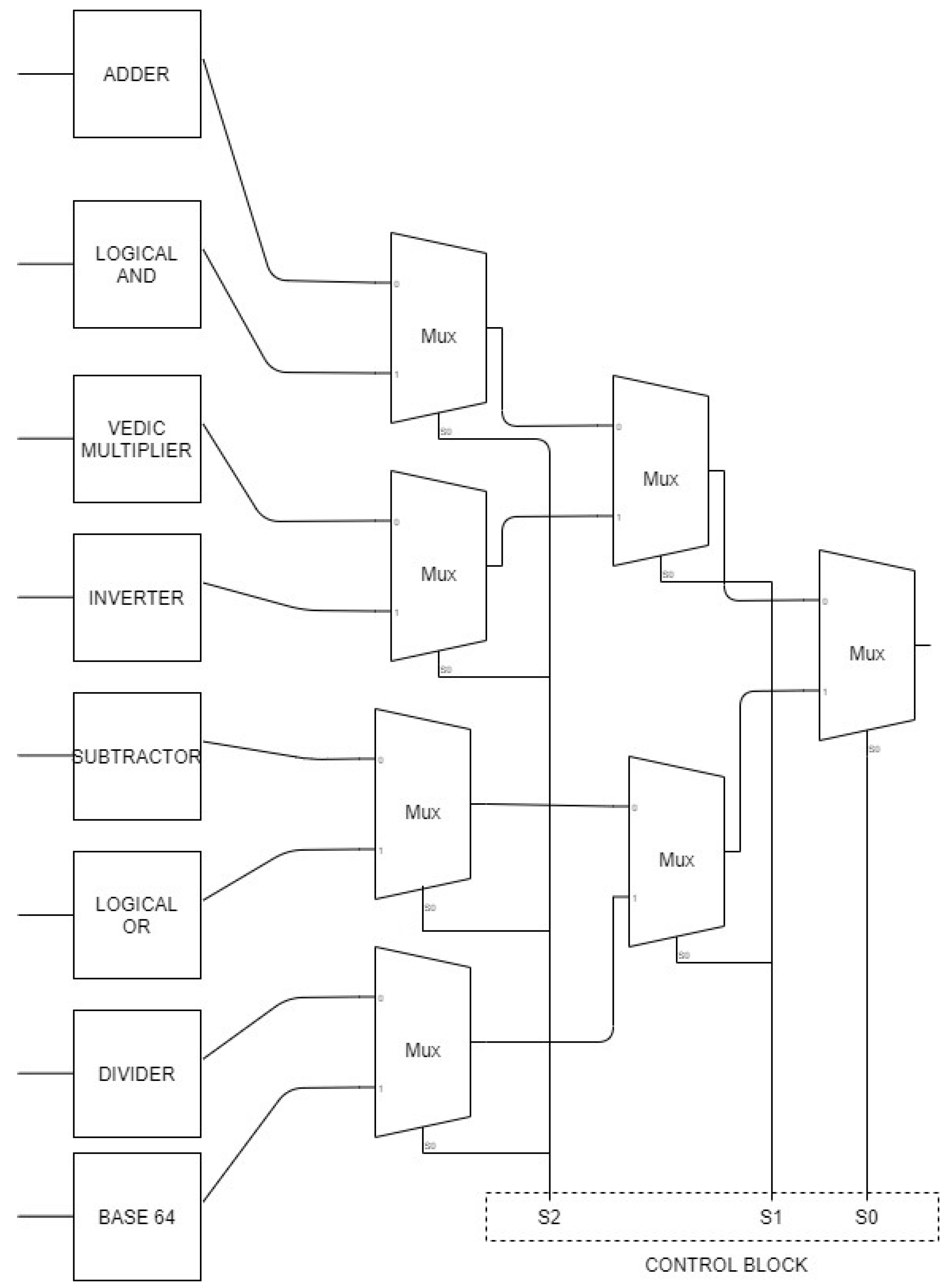
Designing an ALCU can be made more accessible by giving it a modular structure, where one can add various manageable blocks to be reused later. This ALCU consists of three blocks: arithmetic blocks, logic units, and compression blocks. Arithmetic blocks consist of a 16-bit addition module, 16-bit subtraction module, 16-bit division, and 16-bit multiplication module. The logic block consists of a 16-bit Bit-wise AND module, 16-bit Bit-wise OR module, and a 16-bit inverter module. The compression blocks use a 16-bit Base64 encoder module.
Table 2 summarizes ALCU and its operations, and
Figure 1 shows our ALCU block diagram.
4.1. Arithmetic Block
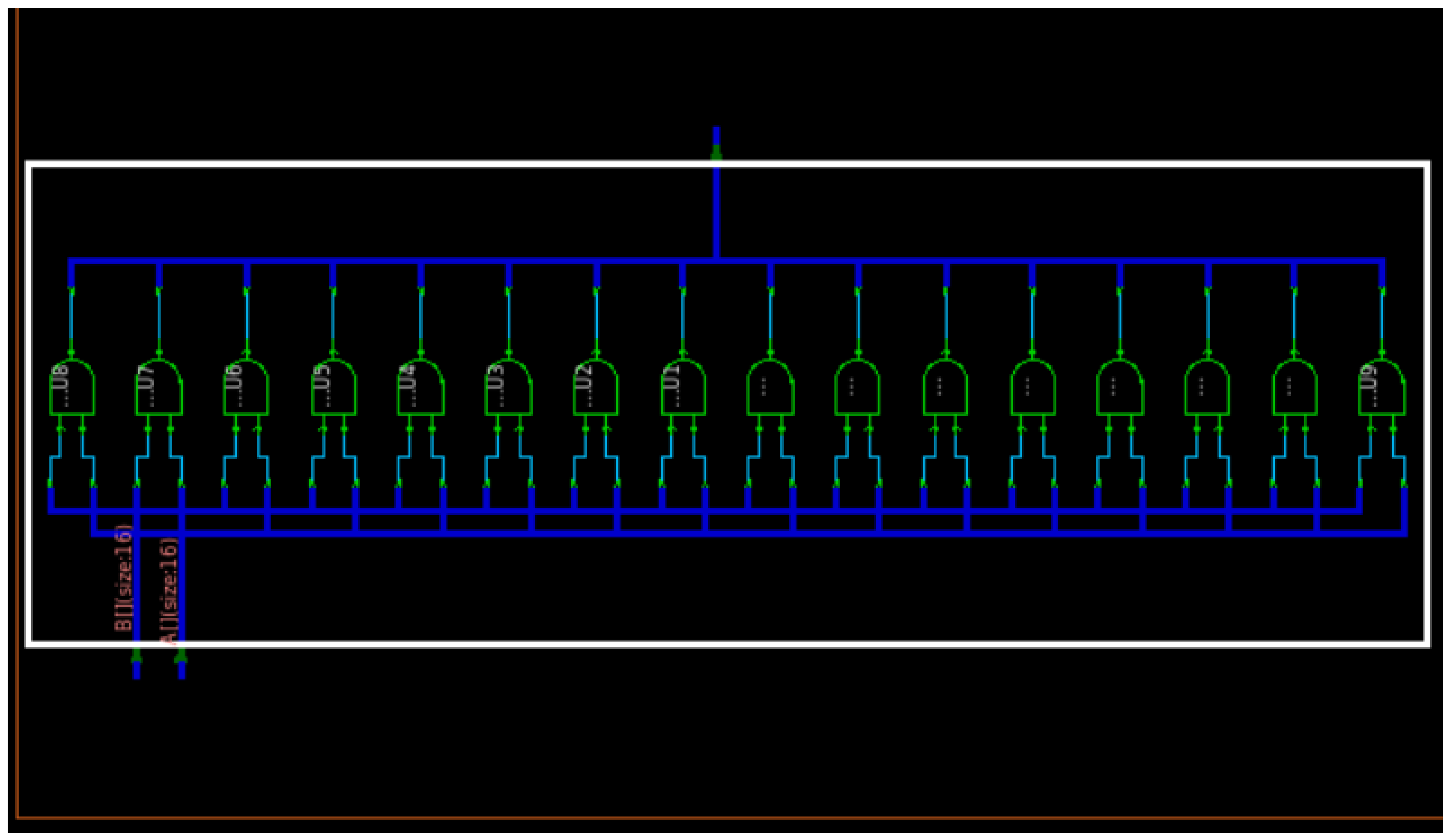
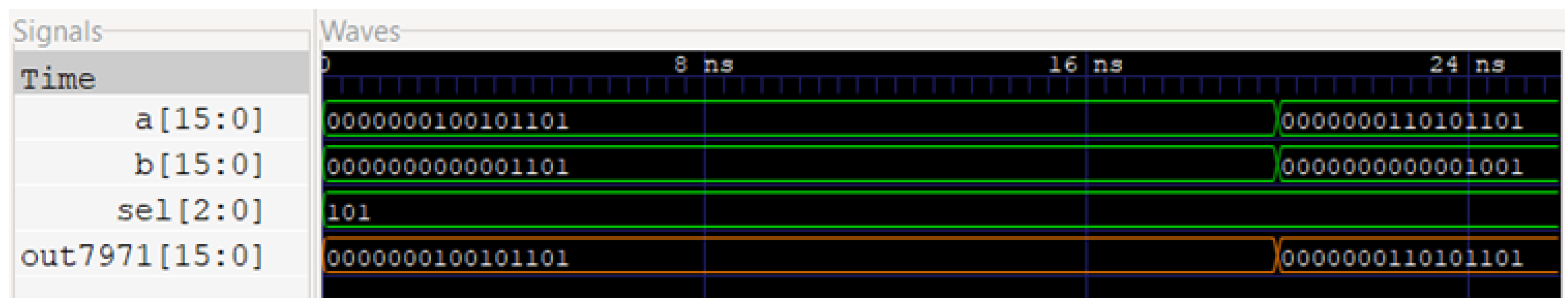
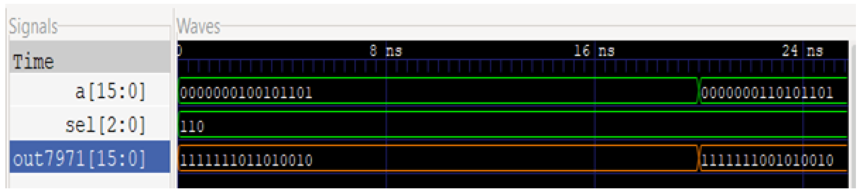
Arithmetic units perform the following functions: addition, subtraction, multiplication, and division. The 16-bit output is received since the input is 16 bits. The arithmetic will only display one output at a time; a selector is required to pick one of the operators. Hence, we use an 8:1 multiplexer with C2, C1, and C0 as control lines; A and B are 16-bit inputs; and Y is the 16-bit output. The selection modes would be:
If Control bits = ‘000’:
Then addition takes place.
If Control bits = ‘001’:
Then subtraction takes place.
If Control bits = ‘010’:
Then multiplication takes place.
If Control bits = ‘011’:
Then division takes place.
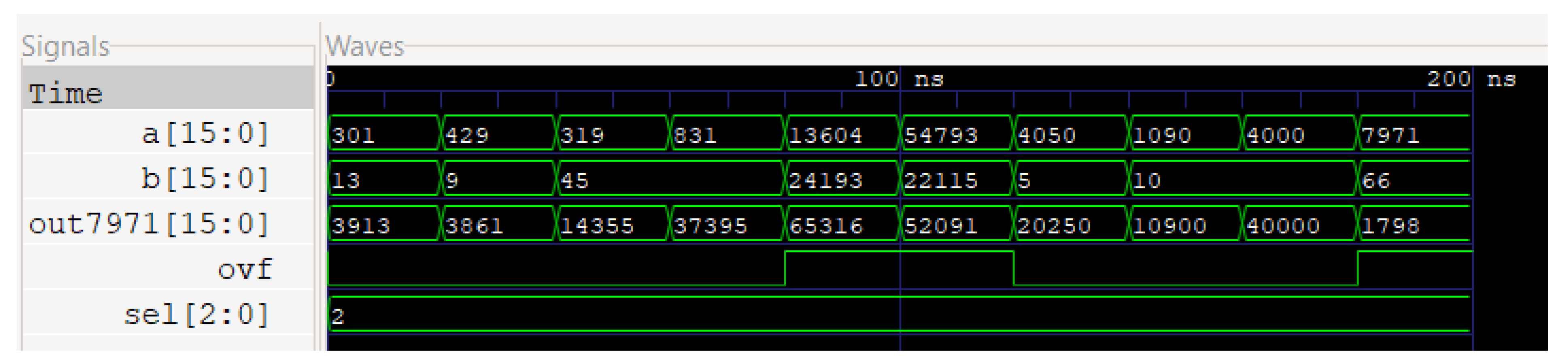
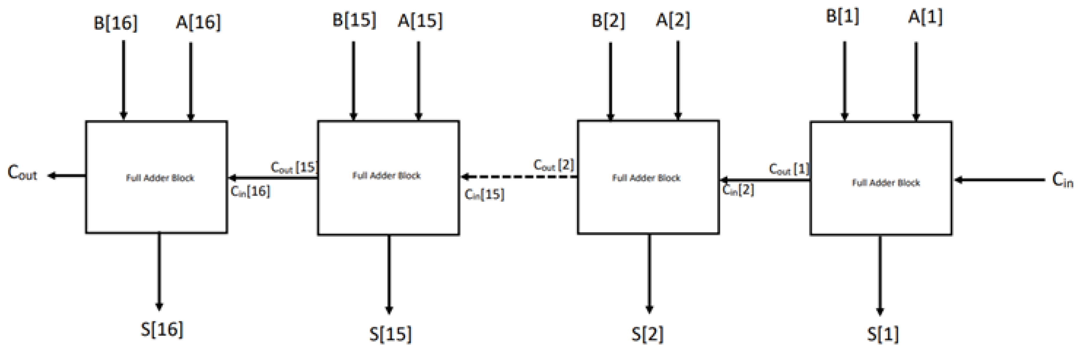
4.1.1. 16-Bit Ripple Carry Full Adder
A full adder is an adder that takes three inputs and outputs two results. The first two inputs are
A and
B, while the third is an input labeled as
as indicated in
Figure 2. The output carry is denoted by
, while the normal output is denoted by
S, which stands for SUM. If “Carry in” is 0, the behavior of a full adder is identical to that of a half adder. However, if “Carry in” is 1, the sum’s behavior is the inverse, and “Carry out” changes into an OR. As long as any of the inputs are 1, Carry out is 1. A full adder logic is designed to accept eight or more inputs to construct a byte-wide adder and cascade the carry bit from one adder to the next. Hence, this design can be used to create a 16-bit binary adder. We cascade 16 full adder blocks together, passing the Carry over from the first full adder to the second [
21], from the second to the third, and so on. Bits of
till
and
till
are given simultaneously as a single bit to each one of the adders, and an initial
of 0 is given. A full adder operation takes place in each block, and Carry is passed along to the following full adder block. The adder blocks individually transmit out the sum of the bits one by one.
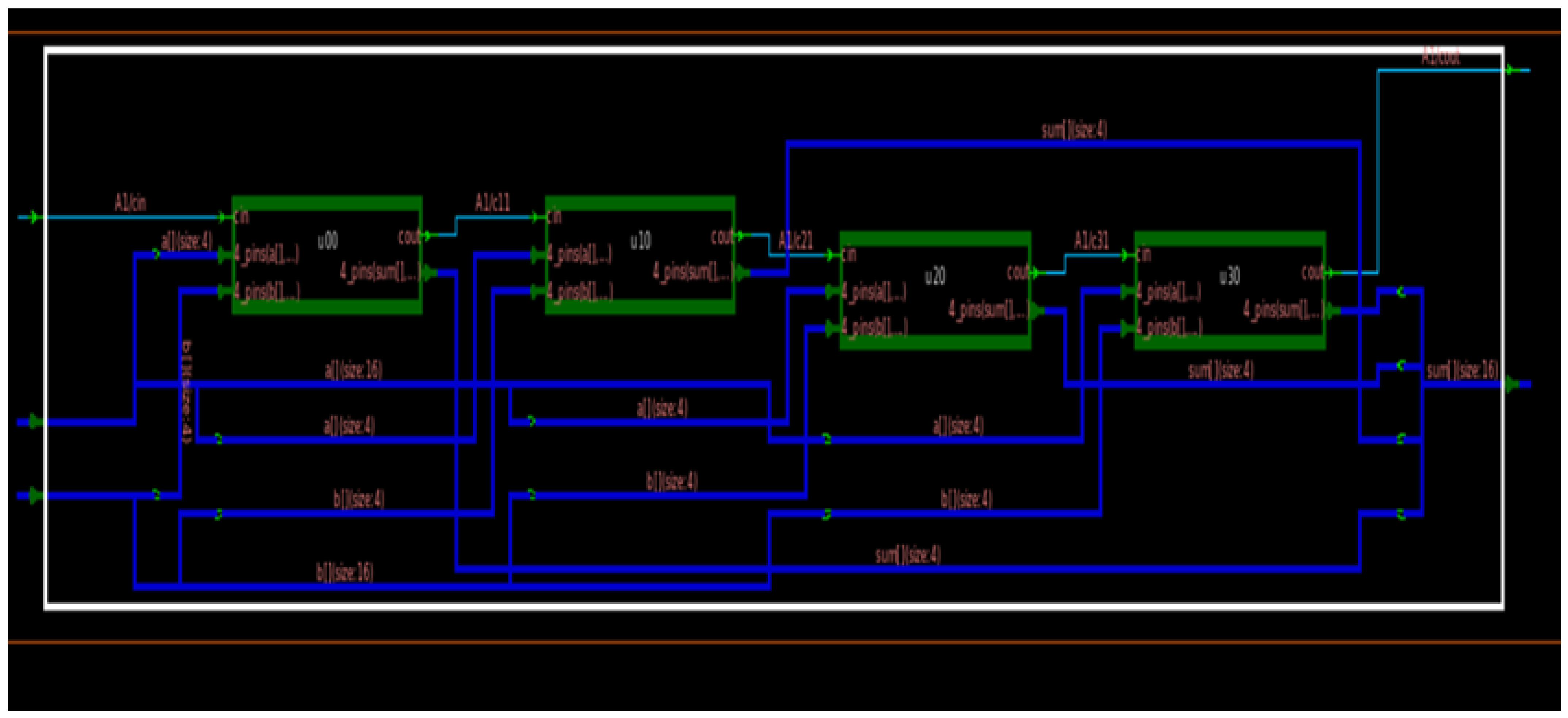
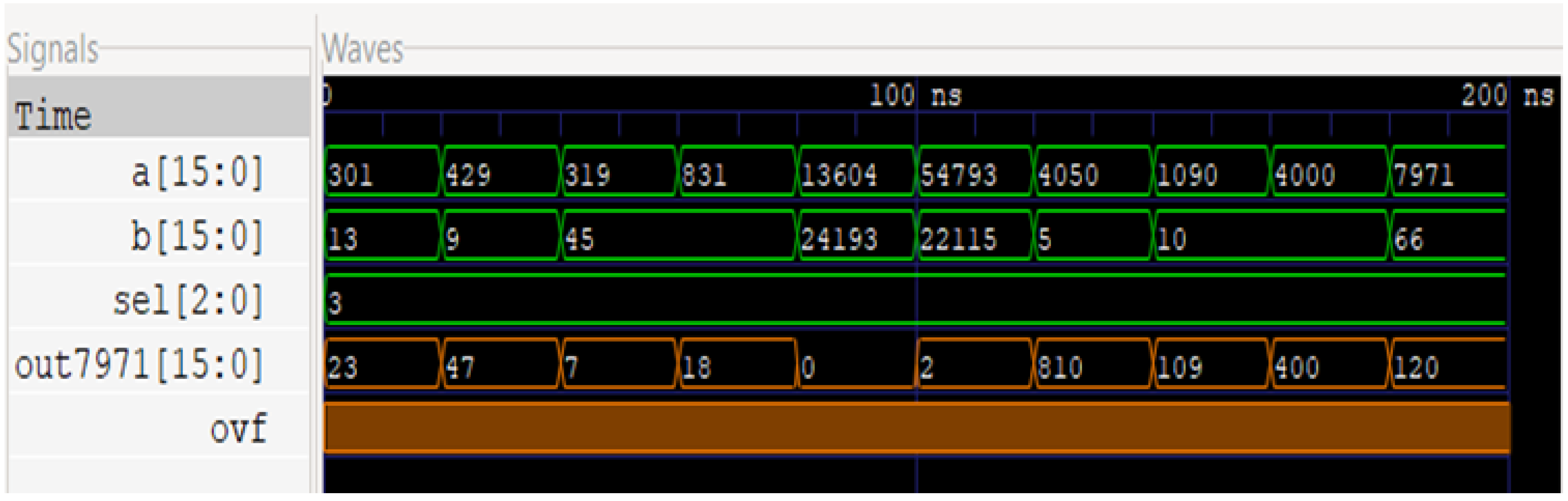
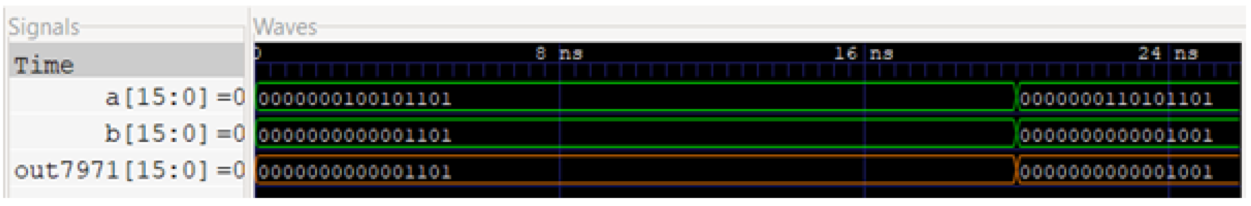
Figure 3 and
Figure 4 show the circuit and waveform results from our full adder implementation.
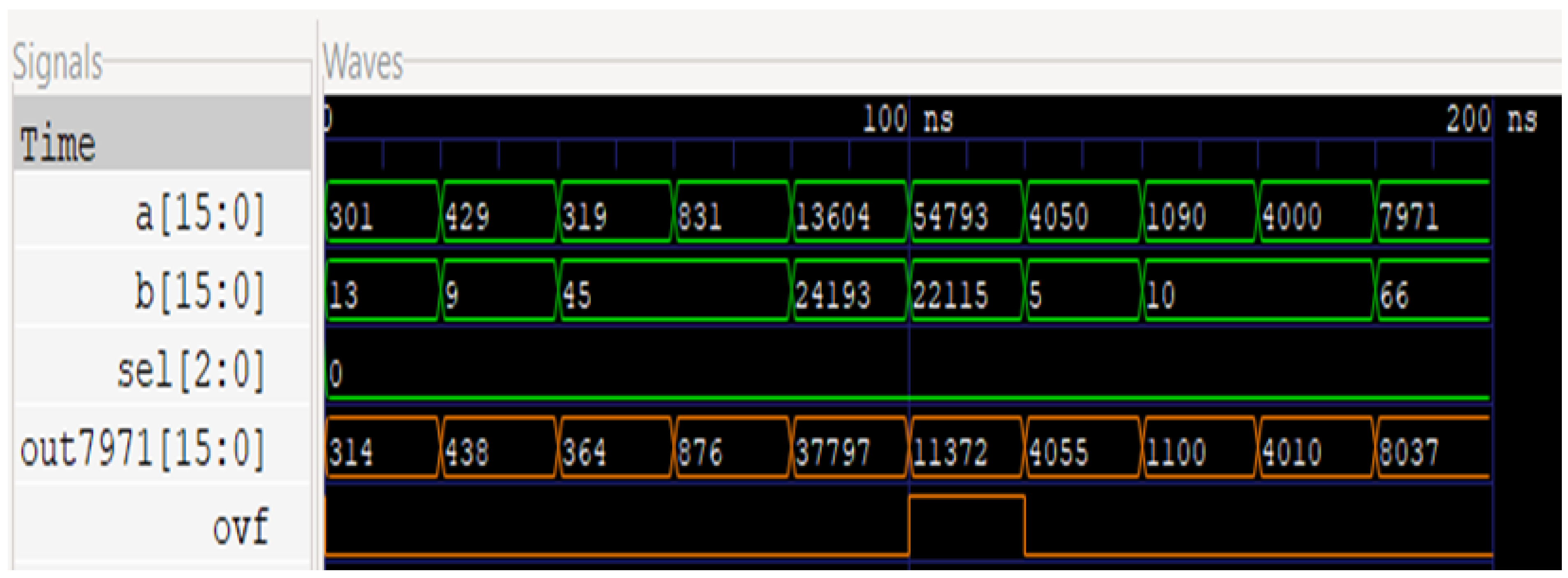
In
Figure 3, we can observe four 4-bit ripple carry adders connected as a single ripple carry adder unit to generate a 16-bit output, along with the final carry output as an overhead.
Figure 4 illustrates the simulated results of this circuit, with the first two waves being the two 16-bit inputs, ‘sel’ describing the selector control signal, and ‘out7971’ as the 16-bit output followed by the overflow bit.
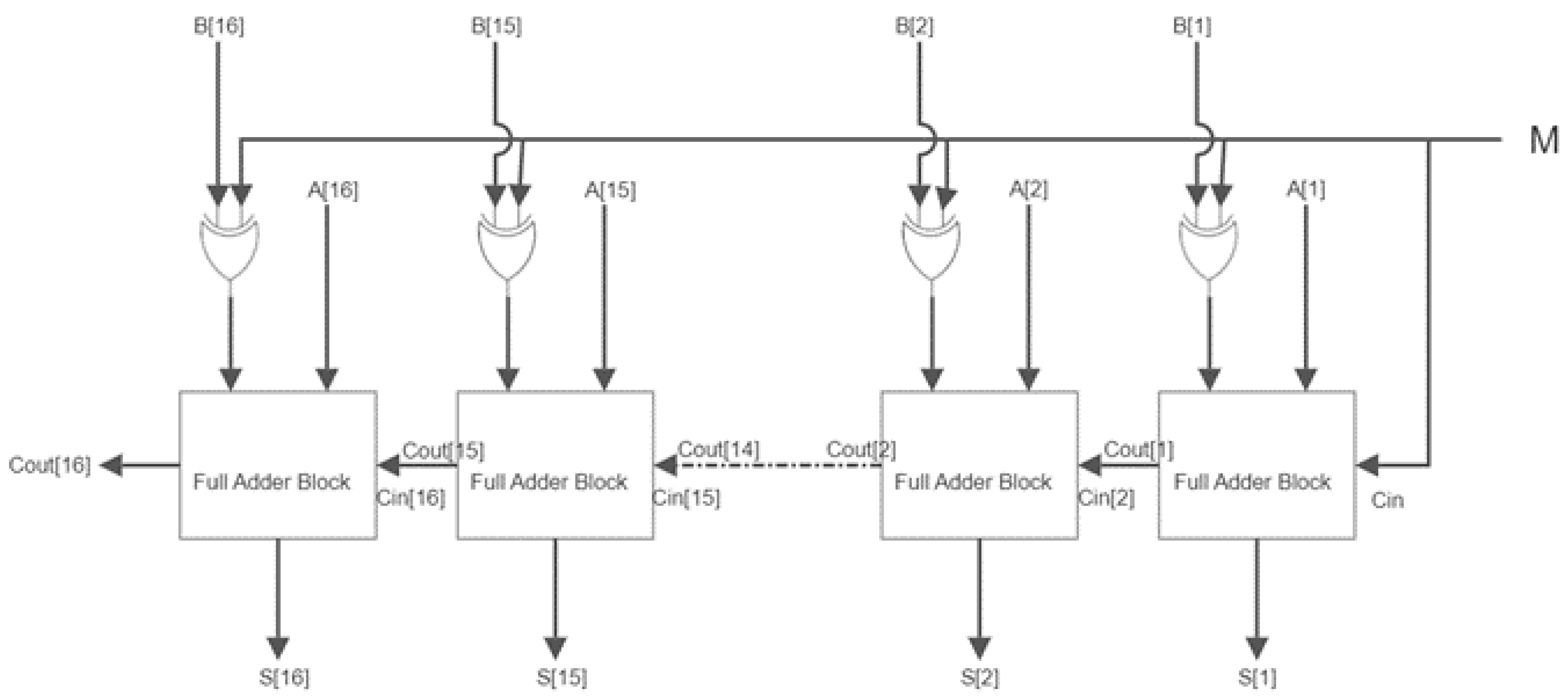
4.1.2. 16-Bit Ripple Carry Subtractor
Binary subtraction is the binary addition of a negative number. Hence, the full adder module can still be used to create the binary subtraction operation with a few changes. Binary subtraction is performed by 2’ complementing the
B bit and adding them to the
A bit as illustrated in
Figure 5. The
M line here acts as the control line. A value of 1 is given from the
M line to each EXOR gate and as the input to Carry in (
) for the full adder block. The ripple carry subtractor can be designed to accept more than 1 bit parallelly to create a bit wide array subtractor. So this means that it could also be used for making a 16-bit carry subtractor. These blocks with a full adder and EXOR cascade together, forming a 16-bit ripple-carry subtractor [
22]. The control line passes ‘1’ as both the Carry in and each existing EXOR gate, which performs the EXOR operation with each of the
B bits (
to
). The full adder block adds the input bits and gives out SUM
S parallelly for each bit (
to
). The overflow is carried forward to the adjacent block as Carry in, so the Carry out for the
and
would be Carry in for the second full adder block. This process carries on till the final block, where the Carry is finally given out as Carry out (
). The acquired sum bits would give the difference between the 16-bit
A array and the 16-bit
B array. This same block can also be used as a ripple carry full adder by giving ‘0’ as input through the control line
M.
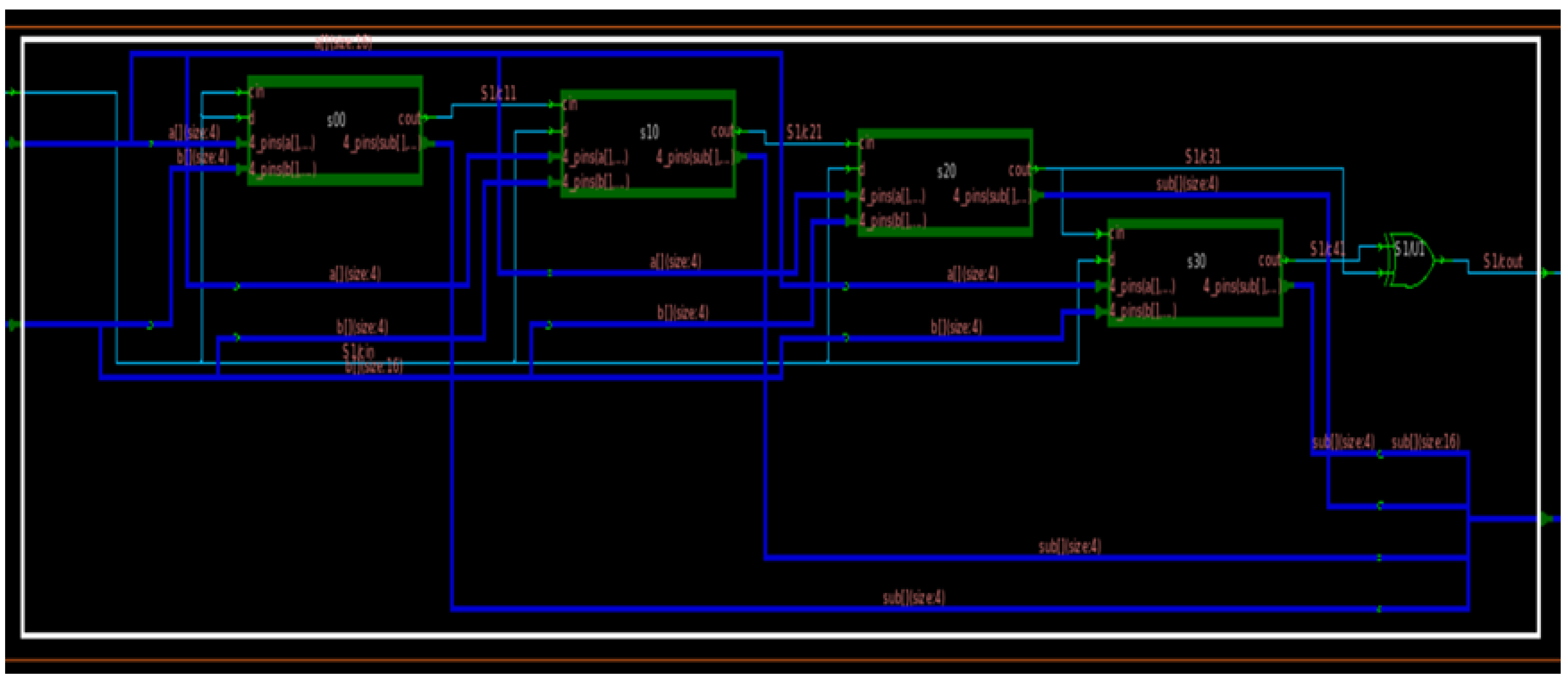
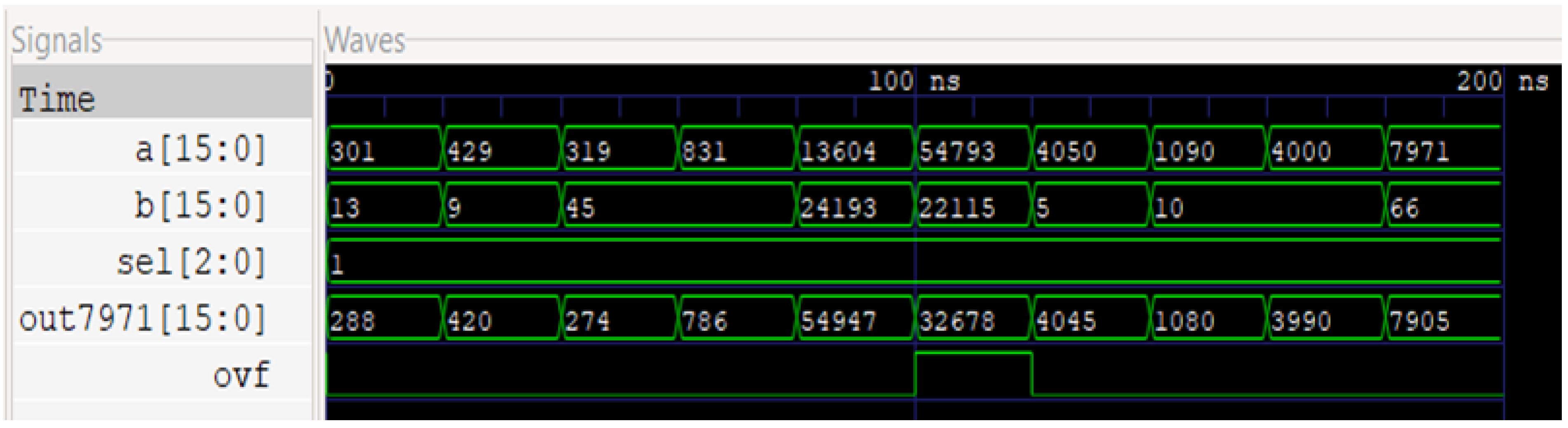
Figure 6 and
Figure 7 show the circuit and waveform results from our subtractor module.
Figure 6, similar to
Figure 3, displays a ripple carry structure, but this time with an additional XOR gate at the second input, this XOR gate is connected to input carry and a second bit to perform 2’s complement. The four visible blocks are 4-bit ripple carry subtractor architectures with an AND gate for the last two carries to generate an overflow output.
Figure 7 demonstrates the waveform that this module generates on simulation. The first two inputs are at the top; the output and overflow are the bottom two waveforms.
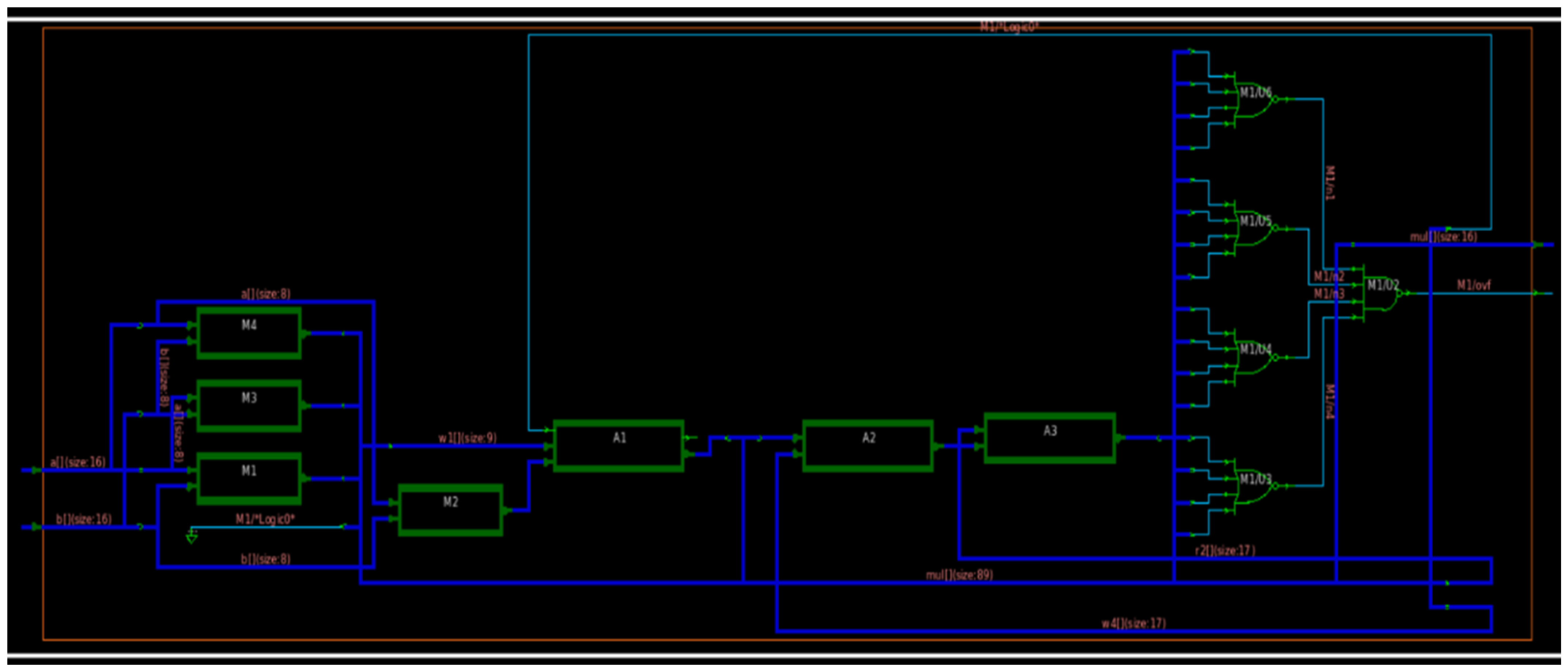
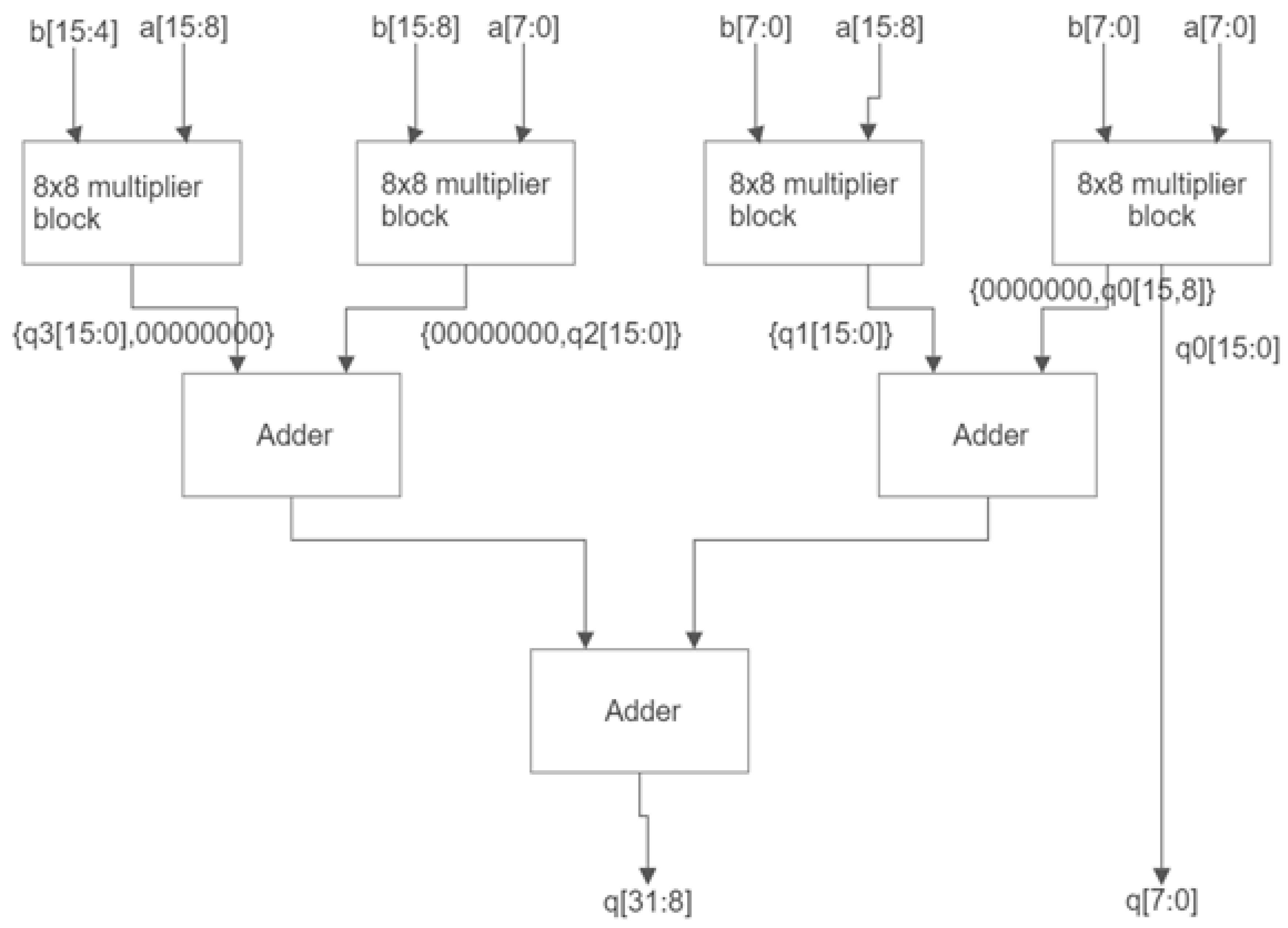
4.1.3. 16-Bit Vedic Arithmetic Multiplier
The multiplication of real, float, and complex numbers is a task that is continuously requested by many internetworking devices. The system calls for these actions are so frequent that deploying specific hardware for this function becomes more appropriate. Just by using the adder module, it is possible to deploy a multiplier in software, but by including hardware into the processor, we can expect to tackle processor delays. There are many types of multipliers; a specific category, fast multipliers, involves the least delay result generation. We have the Vedic multiplier [
23] among these fast multipliers. Contributions to improving area efficiency and power efficiency for implementing a Vedic multiplier in very large-scale integration (VLSI) have grown in popularity these days. In [
24], we can observe research integrating the Vedic multiplier into a reduced instruction set computer (RISC) processor. The path delays can be modified based on how efficiently the adder block behaves in a multiplier. Many researchers modify the adder block and keep the general Vedic multiplier structure constant to improve the multiplier’s area, power, and delay characteristics [
25,
26,
27].
A binary multiplier is an electronic circuit used to multiply two binary numbers. This involves a technique of partial multiplication, which is then followed by being added together to obtain the final result. Contrary to actual multiplication in processors, which is just “Repetitive Addition”, Vedic multiplication is efficient and fast because it does not require “for” loops.
Figure 8 shows the block diagram of a 16-bit multiplier, and
Figure 9 and
Figure 10 show the circuit and waveform results from our multiplication module.
If we observe
Figure 9, we can notice that it is generally divided into two blocks. The first half shows the adder structures to generate the multiplication output. The next is a complex OR gate structure that produces an overhead.
Figure 10 is the waveforms for this structure following a similar structure as its previous blocks.
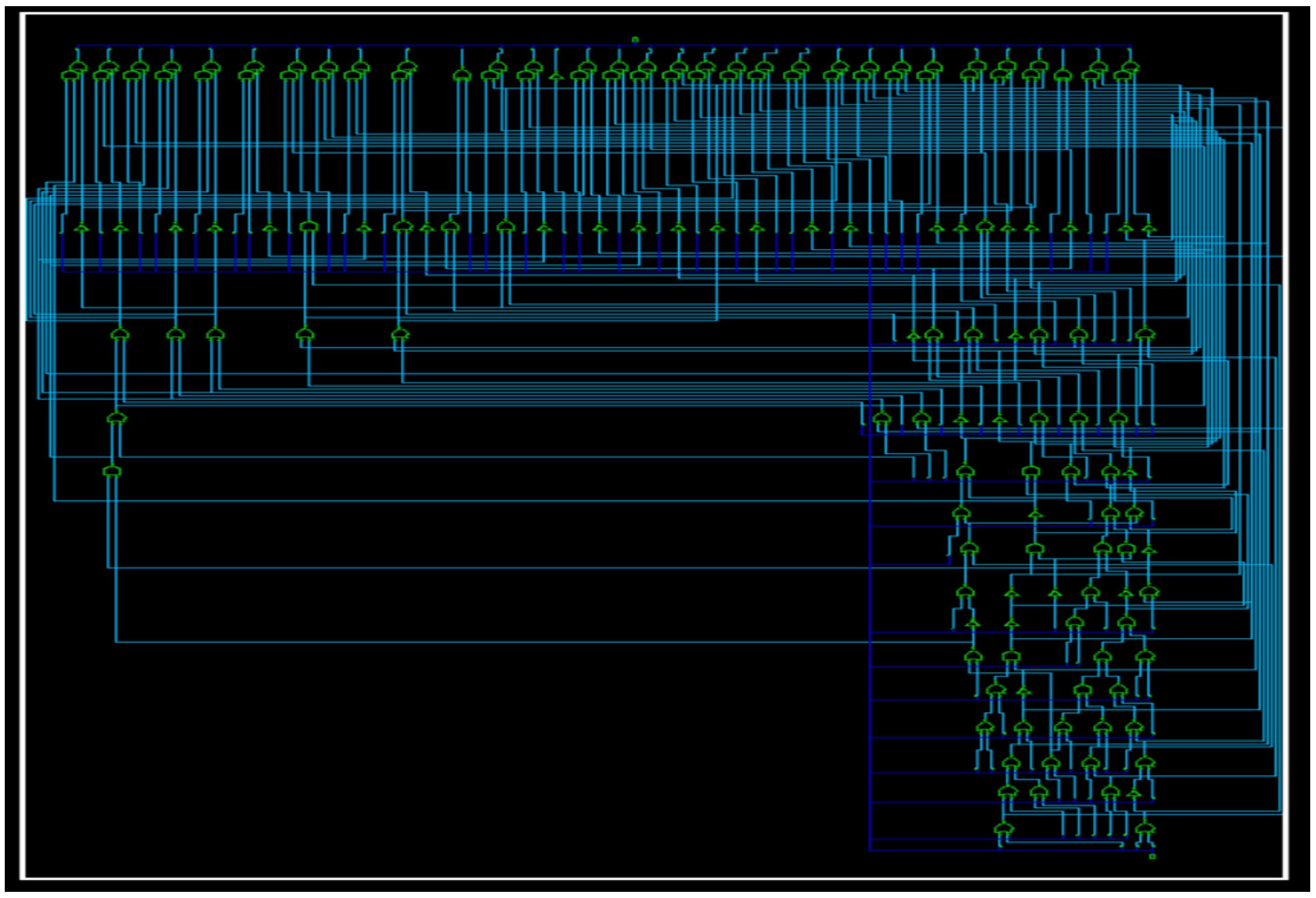
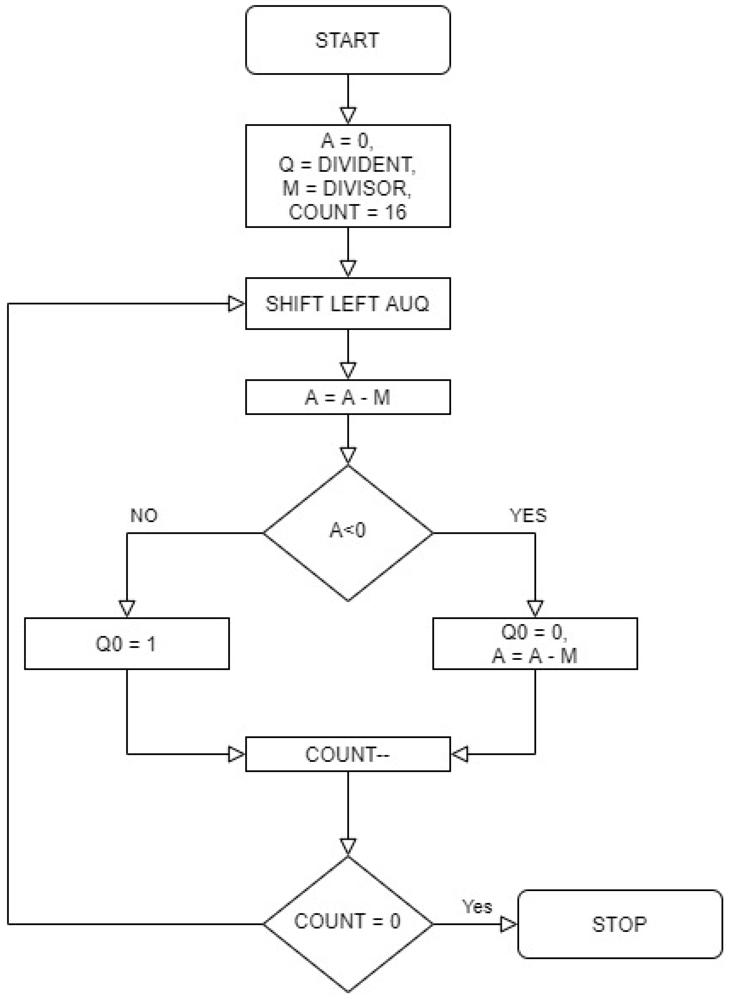
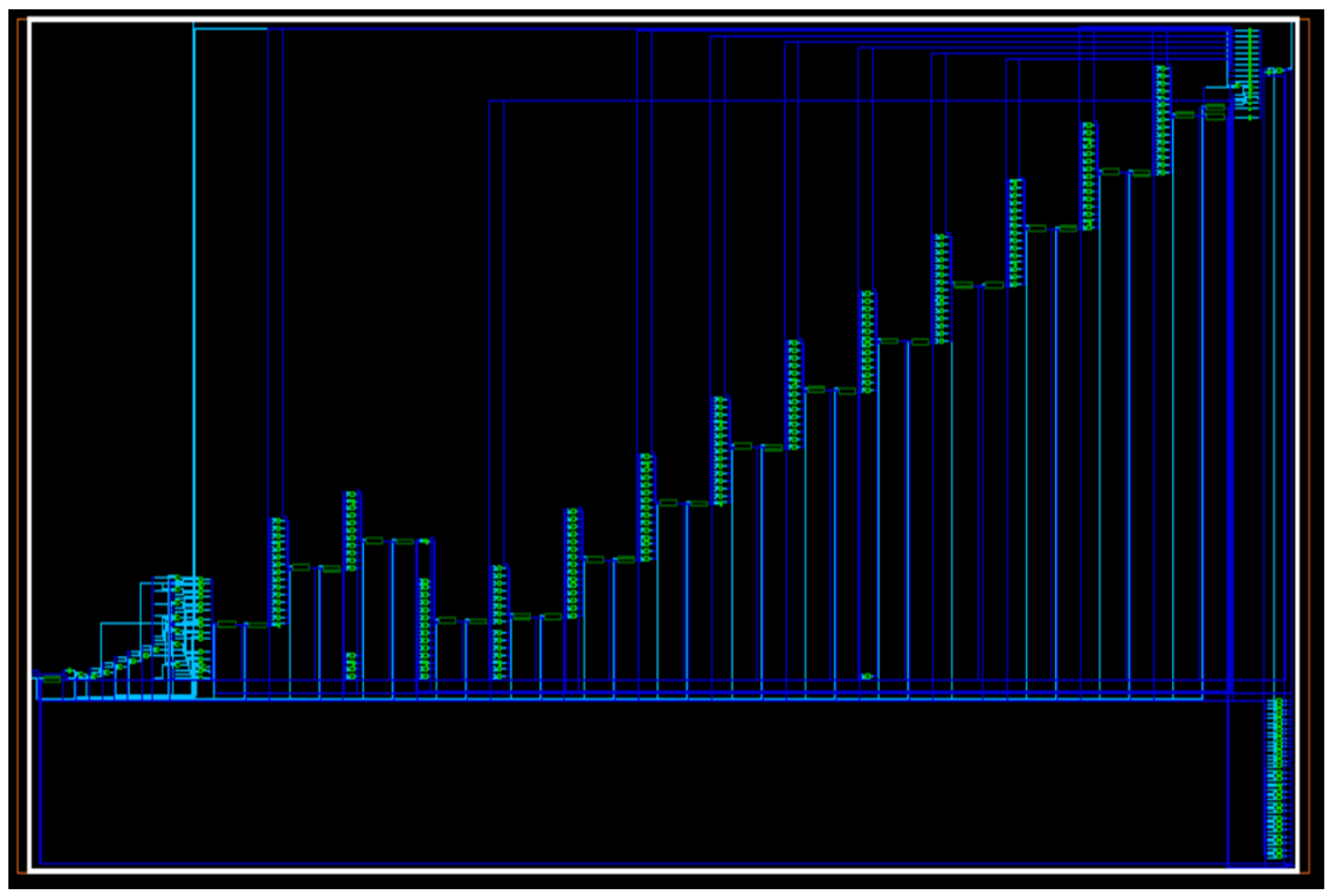
4.1.4. 16-Bit Restoring Divider
Division is one of the fundamental arithmetic operations; it could be on the application layer using a subtractor and adder. However, we decided to integrate it into the hardware to improve efficiency and speed. To integrate it into the hardware, we have taken the algorithm for a famous approach called restoring division for an unsigned integer. Our hardware division in this paper can only deal with unsigned integers. The next upgrade could be to improve it to involve signed floating numbers. The flowchart for this algorithm is illustrated in
Figure 11.
This algorithm required a minimum of four registers of specified parameters to initialize before conducting the procedure. Most of the operations are performed inside registers called accumulator and quotient. Depending upon the sign of the accumulator, the initial value is restored, henceforth getting its name as a restoring divider. There is a special register working as a counter, and this counter is initialized based on the bit length of the operation. In our case, this register is given a decimal value of 16. This algorithm can provide the reminder and quotient, but only the quotient is taken as output for our ALCU. This module also lacks an overflow output. This algorithm’s most intriguing aspect is converting it into a working circuit based on gates. The Verilog syntax for converting this algorithm into a structural code would be highly complex. Hence, it is coded into behavioral code and synthesized. This synthesis is capable of generating a structural netlist for the algorithm. This approach does have its pros and cons, the advantages being that the construction of this module becomes relatively simple, but the generated structural syntax might not be well optimized to use the least amount of logic. Compared to many other division algorithms, the restoring approach is fairly time consuming due to the operation of restoring a register in every cycle. In the background, it involves many memory allocation and transfer operations. Due to the bit size of 16, this algorithm proves to be sufficient in execution time and efficiency. The algorithms that prove more efficient than a conventional restoring divider are non-restoring, radix-2 non-restoring, etc. [
28].
Considering a circuit capable of performing a restoring division on a four-bit binary number, we can see that at least 15 adders and 15 subtractors are employed, excluding other modules, such as comparators, shifters, and multiplexers. This proves that the complexity improves exponentially for a 16 and above bit divider. On synthesizing this algorithm for 16 bits numeric,
Figure 12 shows our implementation, and
Figure 13 shows the waveform results from the 16 × 16 division module.
As we see in
Figure 12, connections exist on the left side of the circuit, from every other stage to the end stage. This additional structure could be minimized if a non-restoring algorithm is utilized. Typically, this divider algorithm consists of a definite ‘for’ loop; in the Verilog schematic, a for loop can be considered a set of adders aligned with the total count being the integer length. The replication of these adders is what is displayed in the schematic with a staircase arrangement. We have this kind of deduction from the schematic since the divider design is completely based on behavioral design rather than structural. As mentioned earlier, restoring division comes under a category called slow division. Fast division algorithms work a fundamental principle of estimation before conducting the division process; they first estimate a value closest to the quotient and work from there to reach a substantial answer. The estimation approach is always a computationally heavy task to perform. Estimation can be performed in presentation, and the above layers and hardware could be used to perform the rest of the architecture. Restoring division assumes that the result lies between zero and counter initial value. This assumption makes the algorithm go through all the cycles of counter length before generating the correct value. Colossal research is still creating efficient and low latency-based hardware for division. This is because improving such basic aspects of the processor might improve the processor performance to a different standard. We also need to consider the register word length while dealing with restoring division. The register size for a 4-bit division is 5 bits. The algorithm might have an unconventional notation for such divisions as the bit size expands.
4.2. Logical Block
The logical block performs the following operations: logical AND, logical OR, and logical NOT. Depending on the operation selected, it either accepts two inputs or one. It uses the same multiplexing (MUX) as used by arithmetic blocks.
If Control bits = ‘100’:
Then bitwise AND takes place.
If Control bits = ‘101’:
Then bitwise OR takes place.
If Control bits = ‘110’:
Then Inverter operation takes place.
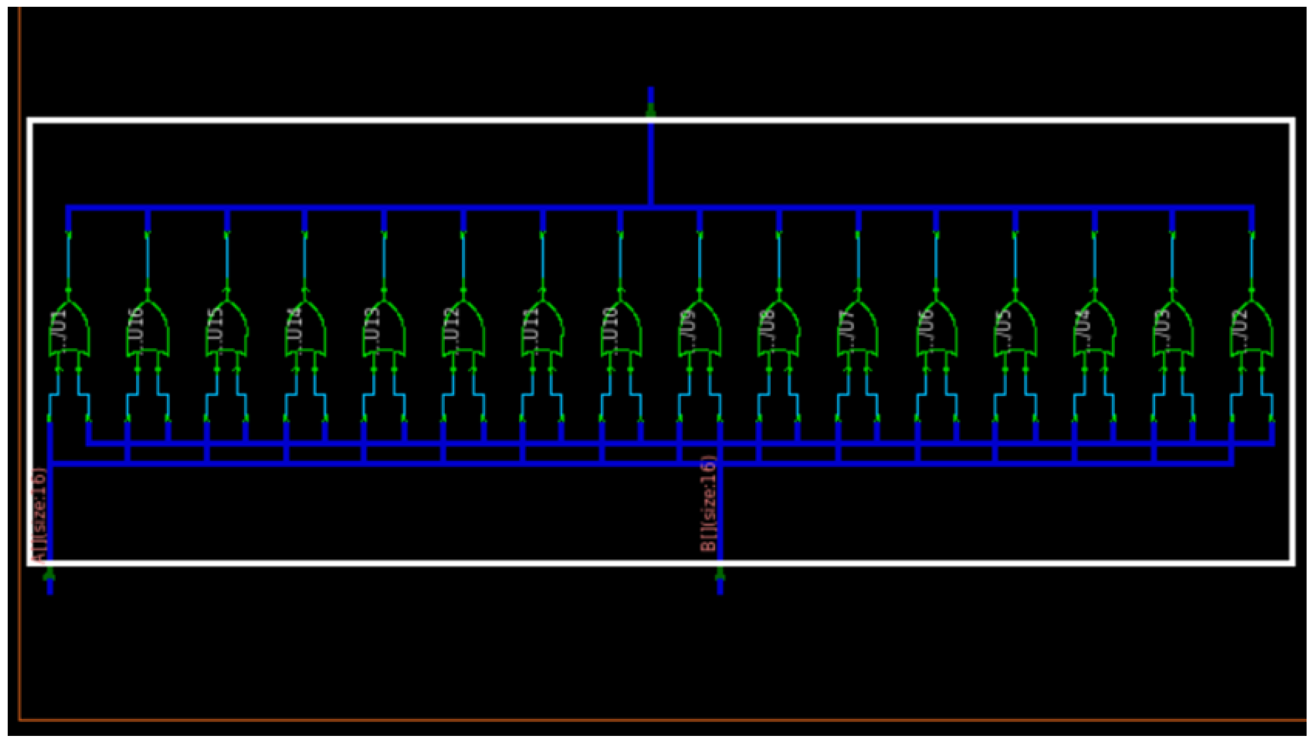
4.2.1. Bitwise AND
Bitwise AND module performs ‘AND’ operation for a given 16-bit input and gives an output for each bit individually. It takes two binary numbers of equal length, resulting in the operation, where each bit from the
A array is compared to its counterpart in
B. Thus, if both bits in the compared location are 1, the bit in the resultant binary representation is 1 (1 × 1 = 1); otherwise, the result is 0 (1 × 0 = 0 and 0 × 0 = 0). The bitwise AND operator can be implemented to clear certain bits (or flags) of a register, where each bit represents a distinct Boolean state. This method effectively stores many Boolean values while utilizing as little memory as feasible. For example, 0110 (decimal 6) can be considered a set of four flags, where the first and fourth flags are clear (0), and the second and third flags are set (1). The third flag can be removed by performing a bitwise AND with a pattern with just a zero in the third bit.
Figure 14 and
Figure 15 show the circuit and waveform results from our bitwise AND implementation.
4.2.2. Bitwise OR
Bitwise OR module performs ‘OR’ operation for two given 16-bit inputs and provides an output for each bit individually. However, unlike the ‘AND’ operation, the binary representation of different lengths still works, considering the excessive missing bits as ‘0’. If both bits are zero, the result is 0; otherwise, it is 1.
Figure 16 and
Figure 17 show our bitwise OR implementation’s circuit and waveform results.
4.2.3. Bitwise Inverter
The bitwise NOT operation module performs an inverter operation for a 16-bit input and provides an output for each bit individually.
Figure 18 shows the waveform results of the bitwise inverter module.
4.3. Compression Block
Base64 is an encoding and decoding technique for converting binary data to the ASCII text format and vice versa [
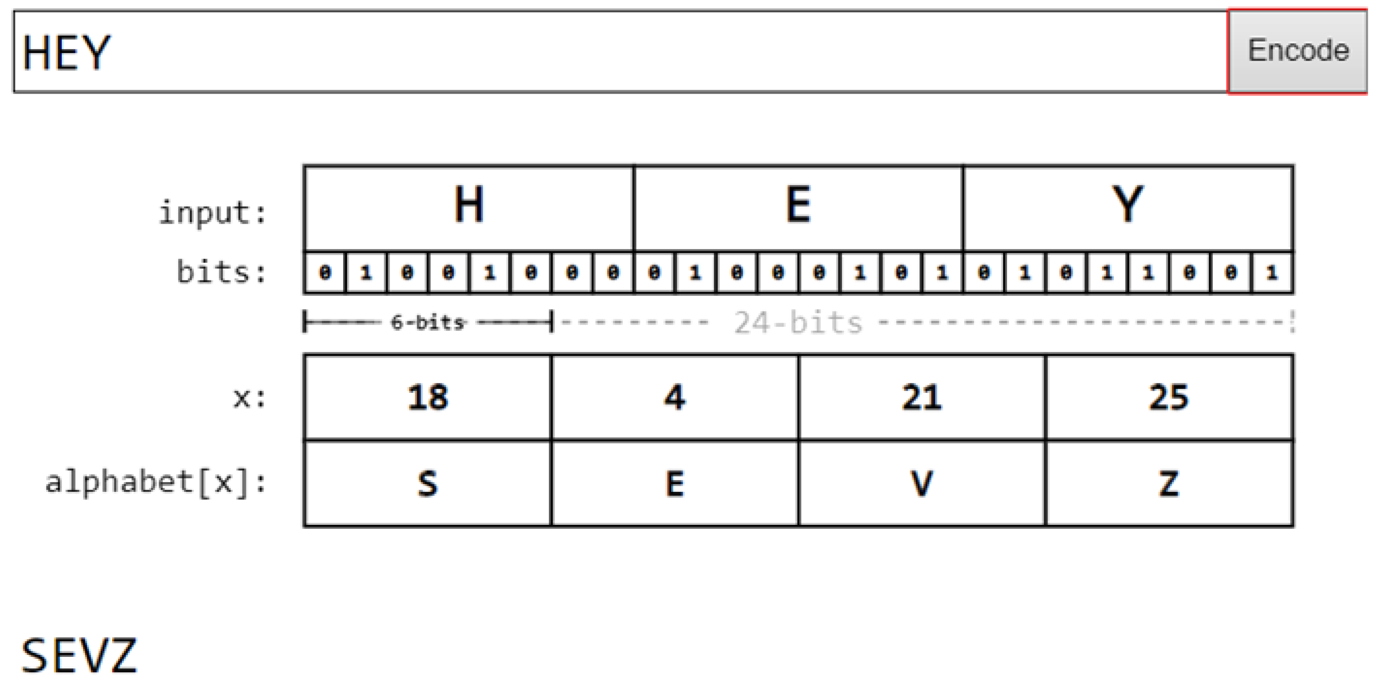
29]. It sends data across a media that only supports ASCII forms, such as email messages and extensible markup language (XML) data. Base64 divides every three bits of binary data into six-bit units. The newly generated data are encoded in a 64-radix number system and seven-bit ASCII text. Because each bit is split into two bits, the translated data are one-third, or 33 percent, more significant than the original data. Files are typically formed up of 8-bit characters. However, for network communication via routers and switches, 7-bit length values are preferable. As a result, delivering the files in an 8-bit format causes file distortion. Base64 encoding is used to overcome this problem. The string is transformed to an ASCII value for a given random string input. These ASCII bits are concatenated together and written in binary 8-bit format. This concatenated number of bits is divided into 6-bit chunks. Each of the 6 bits in the Base64 table is decoded to values in a 7-bit ASCII-friendly format. The compression block consists of a 16-bit Base64 encoder, and this operation takes place when a selection of ‘111’ is given into the ALCU as control bits.
Figure 19 shows the compression procedure.
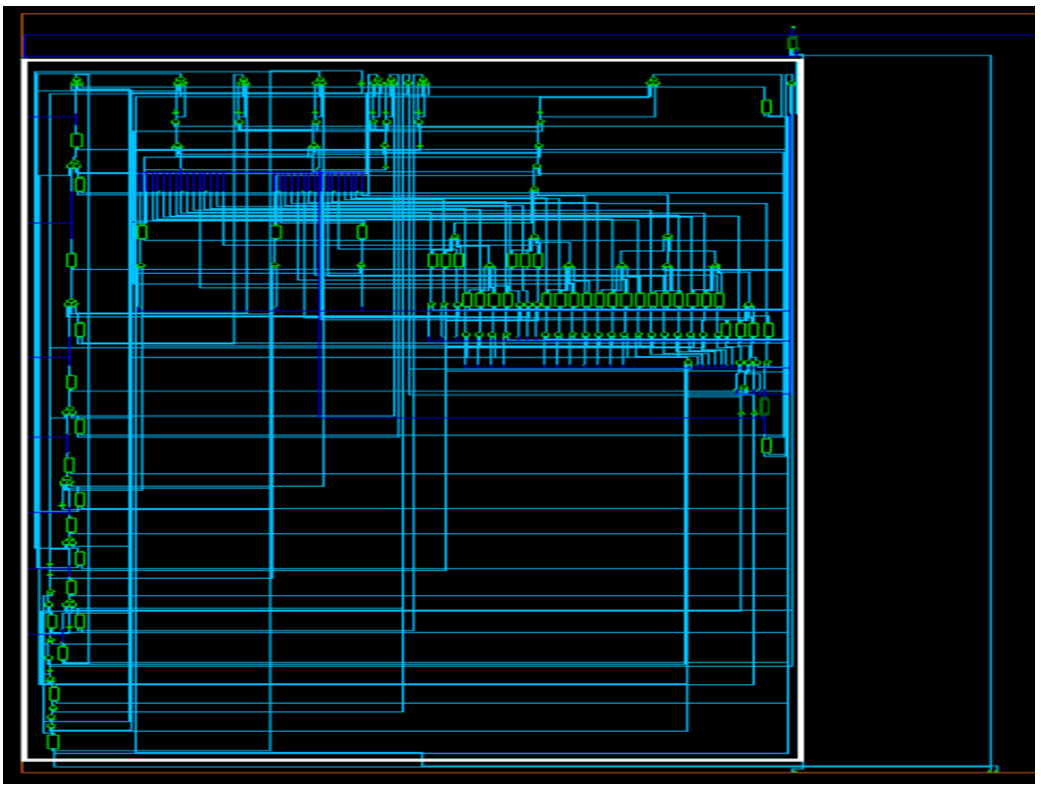
Figure 20 and
Figure 21 show our implementation in Verilog. As we can notice in the figures, this block set has two parts; the first part converts the 8-bit byte data into a 7-bit ASCII encoding, but for transmission convenience, we need 6-bits for BASE 64, and the next part deals with the conversion of this 7-bit data stream to 6-bit stream. In
Figure 20, we notice that the circuitry is complicated, but could be simplified if the output bit length and input length are considered. As mentioned before, the bit length is 16, which means we have two input ports of 16-bit size. The top part of the schematic has 32 ports for this reason. The output of a BASE 64 is only 6-bits in length. Hence, we can notice the ending or the bottom part of a shorter length in terms of ports. Our particular module is designed only to read one input port; hence, the logic levels are only arranged under the right part of 16 bits. In
Figure 21, an ASCII converter is attached at the end of the BASE 64. Many computers from external mediums follow this standard and are easily understood by a computer of any generation. This module is full of registers, similar to a memory unit. It has various register blocks; as we notice, the output is only 7 bits in length in those rectangular blocks. The input comes at 6-bit lengths each; hence, it must store the additional bits before transmission.
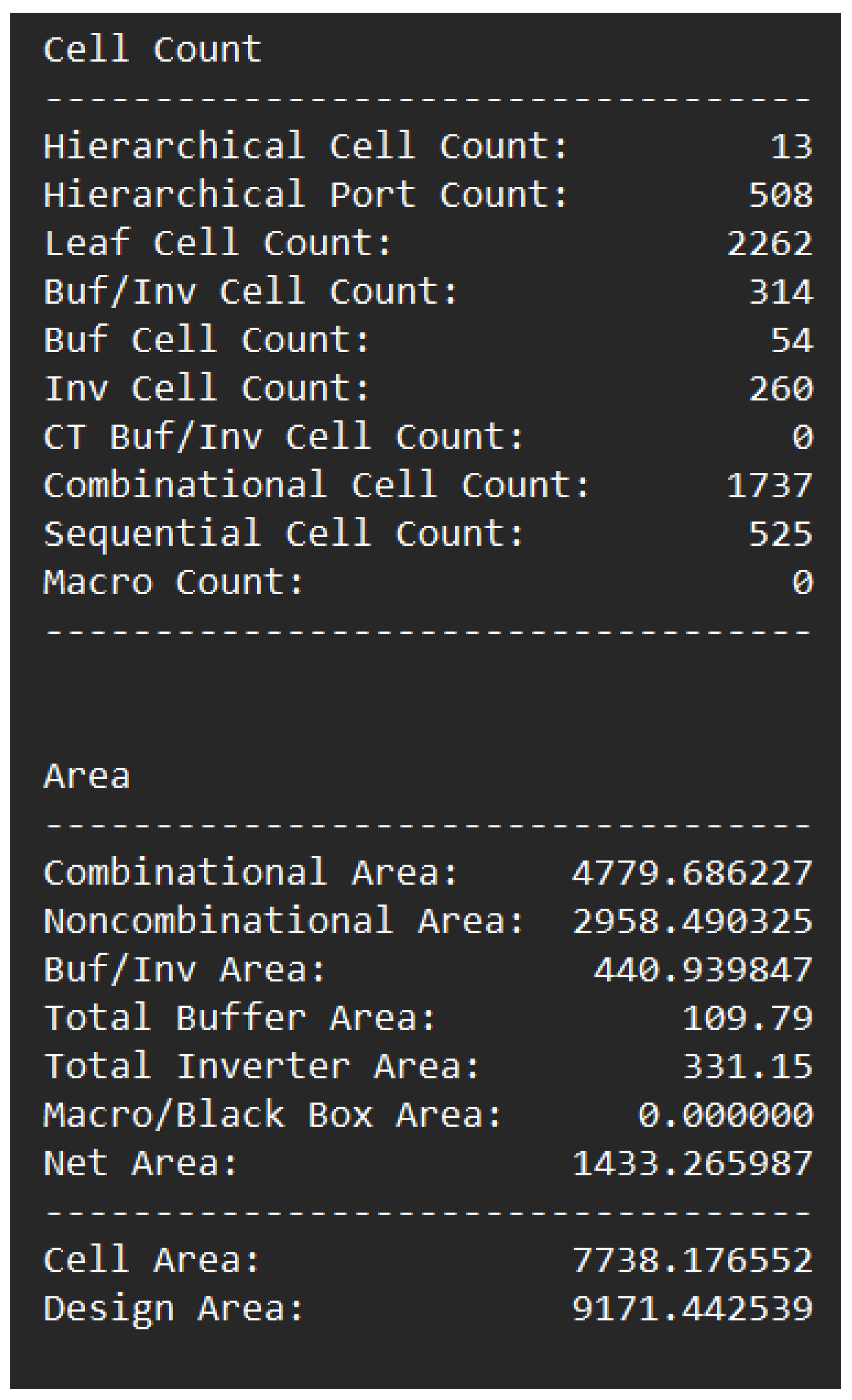
5. Synthesis and Netlist Results
Considering that this is academic research focusing on module development, we avoided many vital steps for hardware design, such as layout, floor planning, and printing. Layout and floor planning are time consuming and often involve expert engineers manually rearranging cells to save area for the processor. This part of the design is very industry specific and becomes harder depending upon the technology used in fabricating the hardware components. A 7 nm fabrication technology might have different initials from those of a 128 nm. Hence the layout is avoided, as it consumes more time and is manufacturer specific. Another vital factor that was overlooked in this research is the delay concept. The code of ALCU considers no delay in any module component. This becomes a more significant problem when the module is produced physically, but due to the academic coverage of the research, we neglected this view. The ALCU designed here is based on a microprocessor without an interlocked pipelined stages (MIPS) architecture. This architecture is considered ancient in present days; there will be more on this in the future scope. The ALCU also consists of only eight components; as per today’s standards, it is optimal to have more components and a bigger ALCU for efficiency. As discussed before, floor planning is an essential step in manufacturing an integrated circuit. Many methods prevail in understanding the shapes and sizes of modules to fit them in the least amount of area possible; some methods include polish notation, sequence pair, etc. [
30].
Synthesis is a process that is conducted to translate the written circuit code into an appropriate schematic. This conversion is highly effective when the code is in a structural format rather than behavioral. Hence, there exist many rules that are to be followed and optimized to generate a working schematic. Writing every integrated circuit into a structural format is complex and time consuming. Many syntheses tools take advantage of automation tools and give a slight degree of freedom to code in behavioral form. For instance, infinite loops and similar syntax are excluded from synthesis, as they make little sense for the hardware [
31]. Netlist is a complete description of all the components involved in the circuitry. It provides a brief statistic on the area consumed, logic levels used, and various active and passive components involved in the specific integrated circuit [
32]. The data logs generated during a netlist generation give us an overview of how the hardware looks when produced.
Figure 22 shows the log data results from our implementation.
For this synthesis, we used a library that produces a netlist based on the semiconductor properties based on the high-voltage threshold. This set of semiconductors is doped so that the threshold voltage is kept higher than the standard threshold. This approach has pros and cons, with the least leakage current but a slower reaction to the provided input. We can use a low threshold voltage for faster performance, but the leakage current increases dramatically. Many electronic design automation (EDA) tools in today’s world consist of libraries producing a multi-voltage threshold netlist. In this category, the components are optimized from the mixture of high- and low-threshold components depending upon their impact and relevance. To cite an instance, in [
33], we can witness a transistor level construction of a carry look-ahead adder with multiple voltage thresholds, achieving low power and high performance.
6. Results Discussion
In this paper, we synthesized an ALCU module and upgraded a conventional ALU module to integrate it with customized IoT-based devices. In this section, we discuss the relation between the results obtained and their application, as mentioned in the literature survey. The synthesis results (referring to
Figure 22) show that their values are reported in micro-meters, which significantly improves over conventional systems. The literature survey comprehensively studies various units used in this module and its architecture. Starting with the adder module, we observe that the proposed ALCU used a ripple carry adder, which is stated to consume a minor area and considerably high delay time. Even though there is a much better adder to tackle both problems, we chose a ripple carry due to its simplicity and smallest area. We expect our module to be an integral part of processors that will be installed in IoT devices, which range in various sizes; hence, area consumption is given a higher priority. The multiplier is a vital component of this module; therefore, more emphasis is placed on considering the proper technique. As stated in the case of the adder, it was our priority to focus more on area consumption. In the case of a Vedic multiplier, as mentioned in the literature review, it consumes less area and power. This construction is very beneficial, as it tackles both issues together. A Vedic multiple presented in this paper can be considered a standard multiplier approach in an ALCU because its small size reduces the system complexity. Even though much smaller area-consuming multipliers exist when 16 bits are considered, scalability will be a severe issue. Due to these considerations, a Vedic multiplier is the best option for an ALU design.
The divider module was added, but no special considerations were laid on this module, as the research of this paper does not focus on improving division algorithms. The concept of integrating a compression block was a significant contribution to this approach. It is conventional to have a compression block separately outside the processor or in terms of software rather than hardware. A hardware module helps this process to happen faster, but it has no involvement from the processor, as it directly deals with the memory unit for data compression. Connecting it with the processor gives the programmer some control over compressing during the program runs. We believe our approach lets the users save time during processing and transfer. The related work states that various compression techniques exist for different data formats. We used a simple ASCII compression block, but in reality, we can use the required compression technique based on the IoT device the processor is developed for. For instance, if a camera is designed, we can use an image compression or video compressor to establish a much more efficient processor. If the compression of the image is included in the processor, we can expect a live streaming facility with lesser data rates. In our case, we used ASCII, which means this processor could transfer text data at higher speeds. This style of architecture would have little importance when storage devices are concerned, but it is helpful when real-time devices are the focus.


