1. Introduction
The revolution of the Internet of Things (IoT) connected era enables an endless field to invent new applications for tracking devices, intelligent sensors, smart agriculture, smart home, etc. The connectivity, range, and battery longevity of those devices depend upon antennas.
Antenna design for wireless devices mainly relies on shaping the geometry of the antenna to make them small enough to fit in the device and multiband to provide operation across several frequency bands [
1,
2,
3,
4,
5,
6,
7,
8,
9]. In some cases, a simple matching network comprising lumped components such as capacitors and inductors is used to fine-tune the frequency response of the antenna. A different approach is addressed by antenna boosters, a tiny non-resonant element where the frequencies of operation are easily adjusted by the designer thanks to the addition of a matching network [
10] (
Figure 1a). This design process is easier and faster than designing an antenna from scratch since the matching network can be efficiently designed using network synthesis tools widely available in most microwave simulators [
11,
12]. Besides its small size (λ/30) and multiband operation, antenna boosters are off-the-shelf SMD (Surface Mounted Devices) components and, therefore, are embedded on a PCB (Printed Circuit Board) of an IoT device using a pick and place assembly process [
13].
Designing IoT devices embedding antenna boosters is straightforward: first, the position of the antenna booster is selected to optimise bandwidth/efficiency. Usually, the corners of the PCB are the best positions [
14]. Second, the matching network is designed using a network synthesis tool [
11,
12,
14,
15,
16,
17,
18]. Finally, the antenna booster on the device is tested in terms of impedance and radiation (efficiency, gain, radiation patterns).
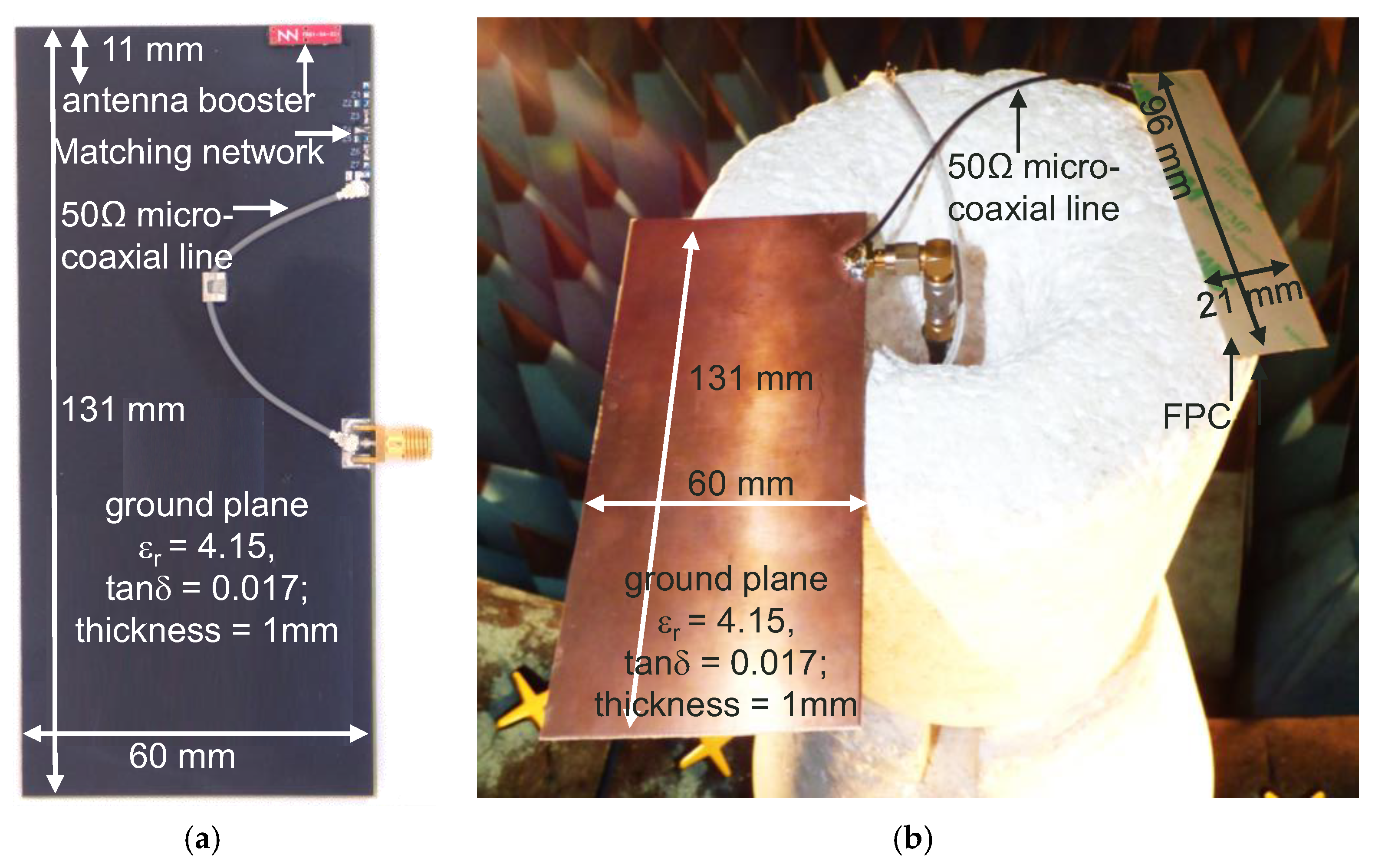
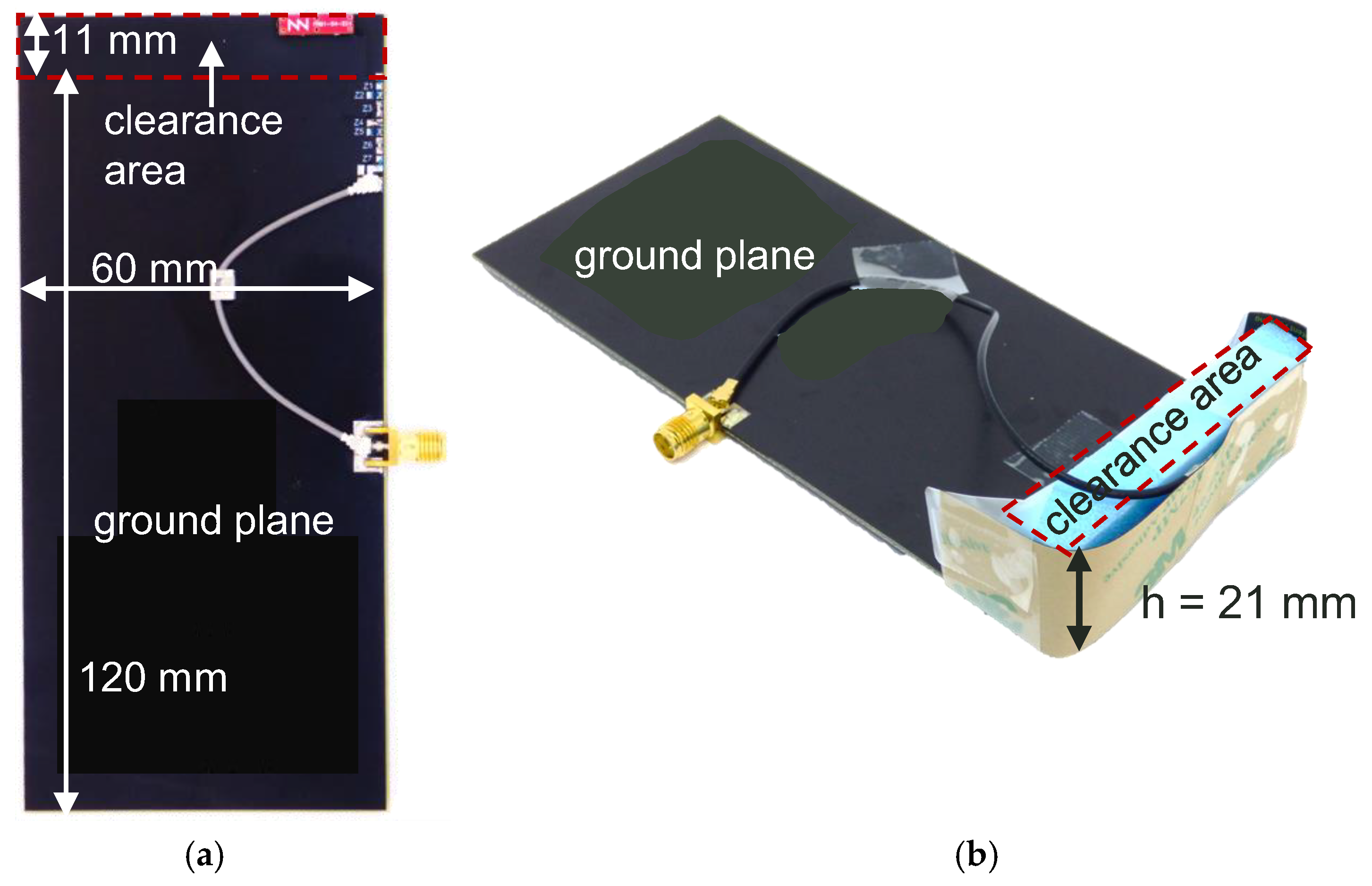
A different alternative to the embedded antenna booster is the so-called flexible printed circuit antenna (FPC antenna) (
Figure 1b). It is based on a conductive element printed on a very thin substrate attached to the device, usually on the plastic cover above the PCB. These antennas come with a 50 Ω micro-coaxial transmission line, so the designer freely places the FPC antenna within the device.
This paper compares antenna boosters and FPC antennas to design IoT devices for cellular frequencies from 698–960 MHz and 1710–2690 MHz in terms of total efficiency η
t. Total efficiency considers both radiation efficiency (η
r) and mismatching as follows [
19]:
From a power perspective, total efficiency is the ratio between power radiated to space and the available power from the source, such as a transceiver. For example, if the power emitted by a transceiver is 23 dBm and the total efficiency is 50%, the radiated power to space is 20 dBm.
This paper is structured as follows: antenna technologies are presented in
Section 2. Results in terms of total efficiency are discussed in
Section 3, considering an FPC antenna at several positions and heights for three different PCB sizes: a big one of 131 mm × 60 mm, a medium one of 95 mm × 42 mm, and a small one of 65 mm × 42 mm. The dependence of the performance as a function of the FPC antenna location is shown in
Section 4. Results for the three different PCBs are discussed in
Section 5. Finally, conclusions are drawn in
Section 6.
2. Embedded Antenna Boosters vs Off-PCB FPC Antennas
The two antenna technologies for IoT devices are compared: antenna booster technology and FPC technology (
Figure 1). The comparison is made at the frequency range of 698–960 MHz and 1710–2690 MHz, where most cellular IoT protocols are allocated.
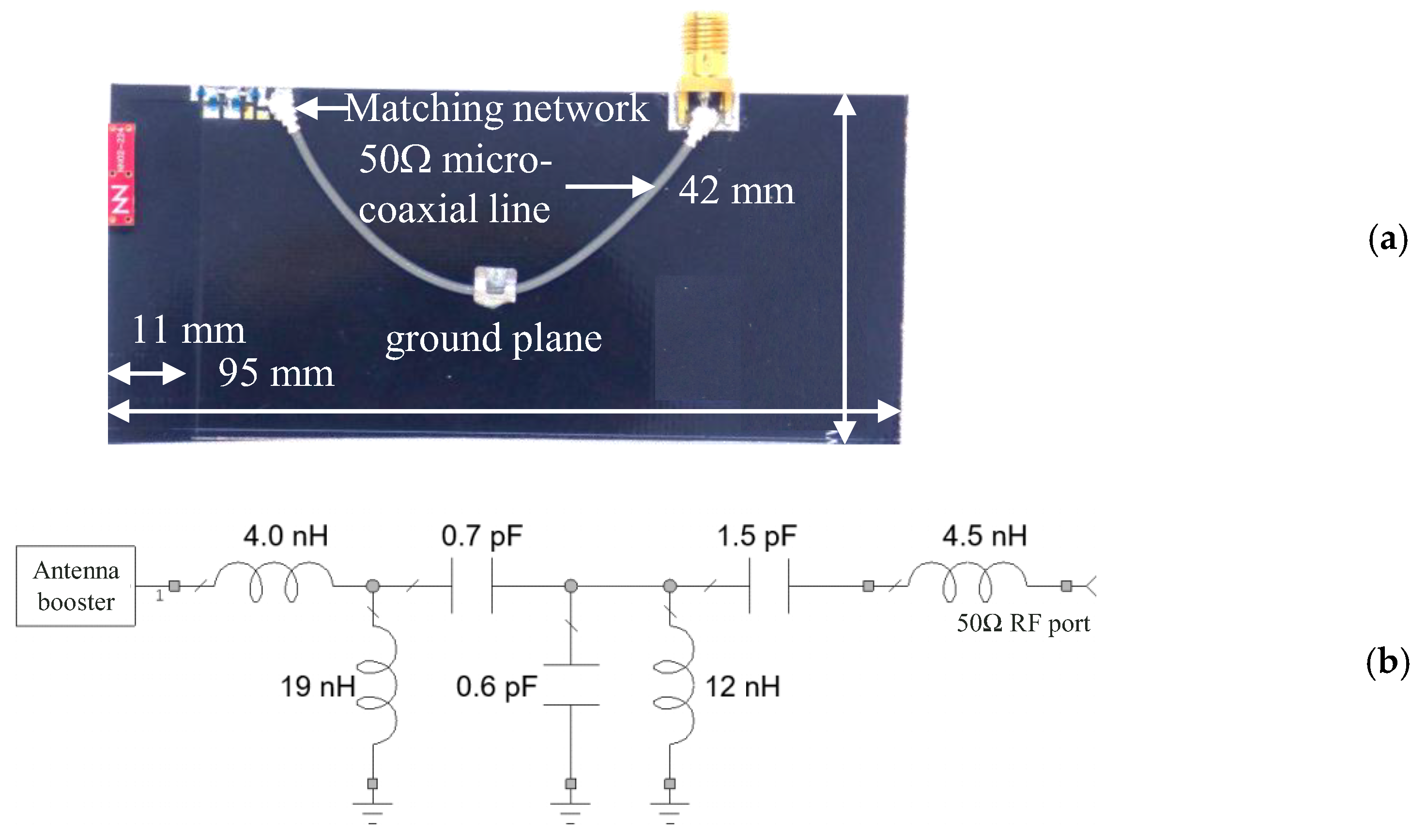
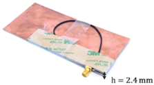
The embedded antenna comprises a 12 mm × 3 mm × 2.4 mm (height) antenna booster mounted on a 131 mm × 60 mm PCB, including a 120 mm × 60 mm ground plane. An antenna booster is an electrically small (λ/30) non-resonant chip antenna like component that is easily embedded on a PCB of an IoT device thanks to its SMD nature and small size (
Figure 1a). Being so small, an antenna booster is off-resonance, needing a matching network to provide a good impedance match to the RF front-end [
20]. By designing the proper matching network following network synthesis microwave tools [
14], a multiband performance is obtained from the booster-ground plane set.
For the present case, the antenna booster is 12 mm × 3 mm × 2.4 mm (height, representing about λ/35 at 698 MHz)
. The antenna booster is available through CST Microwave Studio [
21] for simulation purposes or can be modelled as a 3D conductive parallelepiped with a conductivity σ = 5.9 × 10
7 S/m.
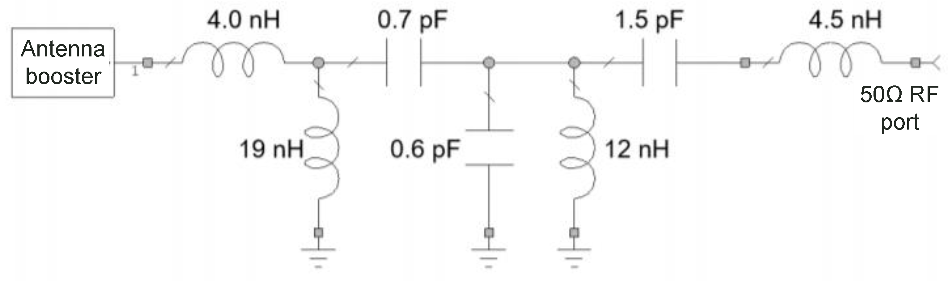
Once the input impedance is measured, the multiband matching network for the antenna booster is easily designed using a network synthesis tool. The network synthesis tool optimises total efficiency (η
t), which is the ratio between the power delivered to the antenna booster and the available power from the generator. Optimising total efficiency and not return loss ensures that the selected lumped components of the matching network introduce low losses. The optimisation process considers available commercial SMD components. Murata SMD 0402 and SMD 0603 high-quality factor components have been used (
Figure 2).
The set-up for the FPC antenna is simple: the FPC antenna is directly connected to the PCB through a 50Ω micro-coaxial which is included with the FPC antenna (
Figure 1b). The feeding location on the PCB is maintained in the same position as the antenna booster. The FPC antenna has a rectangular size of 96 mm × 21 mm, representing λ/5 at the lowest frequency region (698 MHz). This maximum electrical size is eight times more than the size of the antenna booster. In terms of area, the antenna booster (12 mm × 3 mm) is 56 smaller than the FPC antenna (96 mm × 21 mm).
Most FPC antennas rely on self-resonant structures, and therefore, there is no need to use a matching network [
22]. After averaging seven multiband FPC antennas operating from 698–960 MHz and 1710–2690 MHz [
23], the average length and width are 89.6 mm and 25.3 mm, respectively. Therefore, the FPC antenna analysed here is representative of an average FPC antenna.
To compare the performance of both antenna technologies, total efficiency is measured in an anechoic chamber (Satimo Stargate-32) using 3D pattern integration (
Figure 3). Since total efficiency η
t (Equation (1)) considers radiation efficiency and impedance match, η
t is used as a figure of merit for comparison purposes.
Total efficiency shows similar average values (
Table 1). For the FPC, several off-PCB locations have been tested to get the best performance (
Table 1).
Since off-PCB is not the typical situation in most IoT devices requiring an internal antenna because the IoT device size is as large as the PCB, the following section addresses the impact of the FPC antenna on the PCB.
3. Performance Analysis for On-PCB Conditions
Once the off-PCB results for the FPC have been presented, the FPC is embedded on the PCB, considering several heights and positions. Three situations have been considered: a big PCB of 131 mm × 60 mm, a medium PCB of 95 mm × 42 mm, and a small PCB of 65 mm × 42 mm. Since IoT devices should be compact, the size of the device is typically as large as the PCB and thus not leaving space for having the FPC antenna off PCB.
3.1. PCB 131 mm × 60 mm
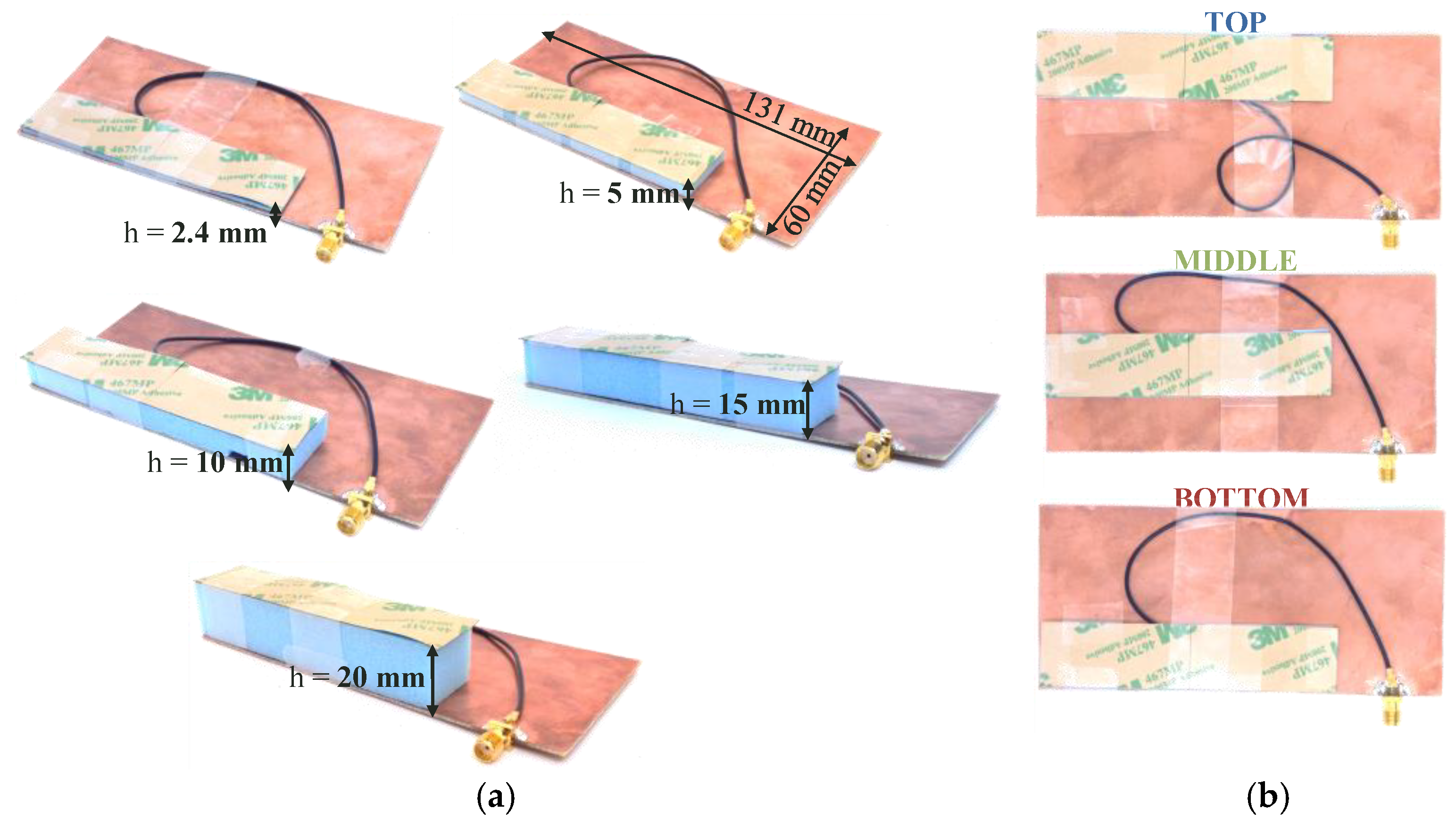
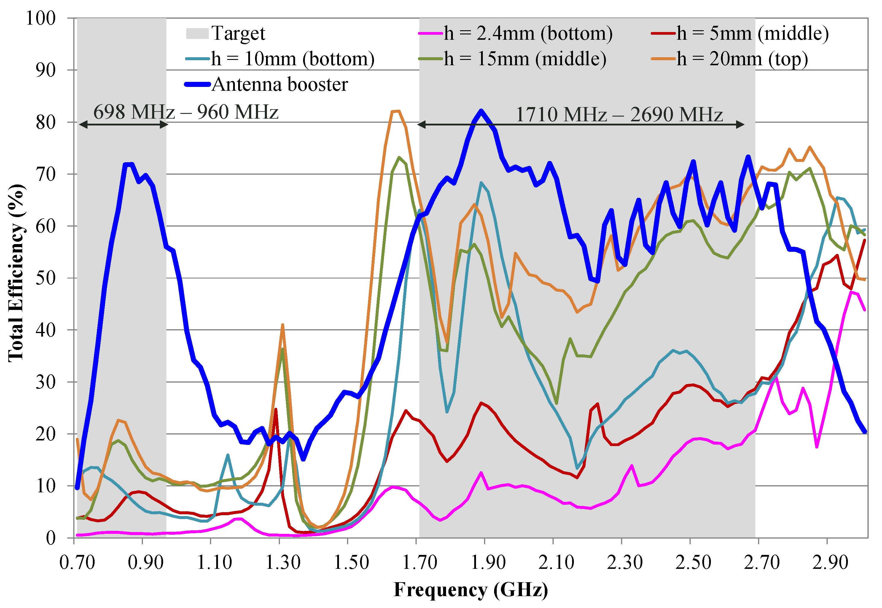
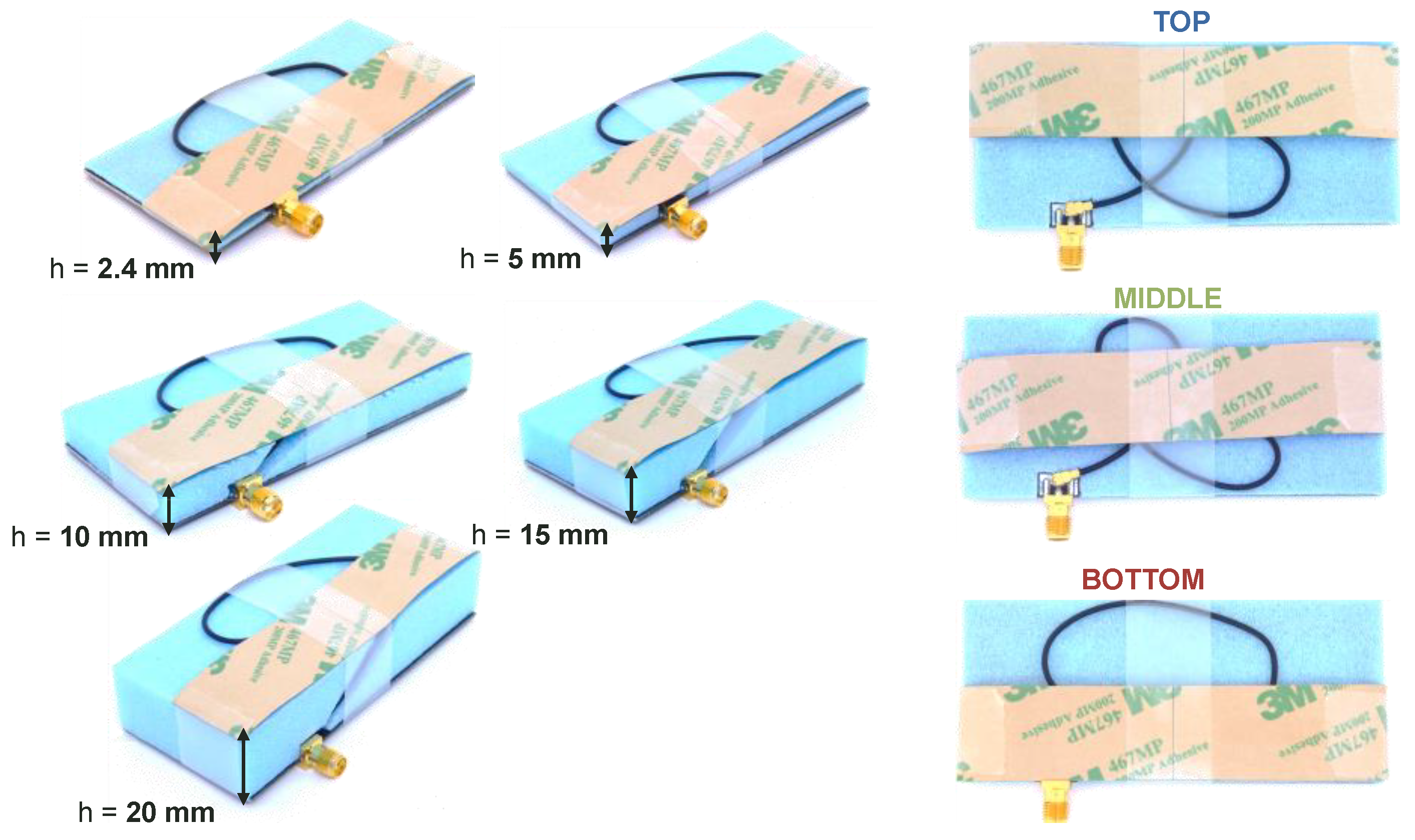
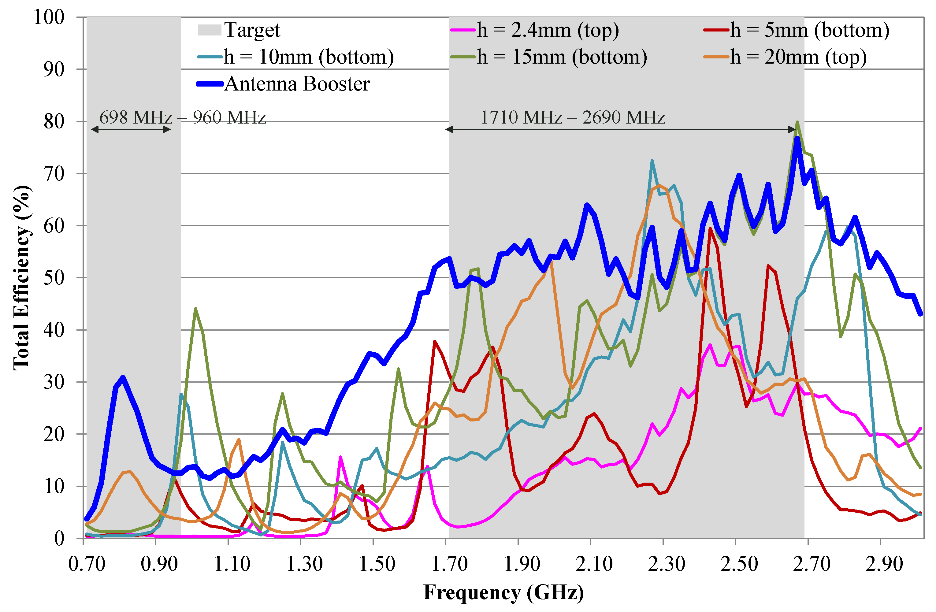
Several heights of the FPC above the ground plane of the PCB have been considered: 2.4 mm (the same height as the antenna booster), 5 mm, 10 mm, 15 mm, and 20 mm (
Figure 4). No more cases have been considered beyond 20 mm since IoT devices should be small and present slim profiles. In this sense, 20 mm is regarded as a limit.
Besides height, different FPC antenna positions have been analysed since the IoT designer has any degree of freedom to allocate the FPC antenna on the device. Three positions have been considered: the top edge, middle, and bottom edge (
Figure 4). Therefore, for the FPC antenna case, there are five height cases and three positions. As a result, there are 15 different measurements. To simplify the results, the best location among the top, middle, and bottom edges in terms of total efficiency is represented for each FPC antenna height. As a result, there are five total efficiency measurements, one per FPC height and one total efficiency measurement for the antenna booster (
Figure 5). This procedure is repeated for the medium and small PCBs.
When mounted on the PCB, total efficiency results for the FPC antenna drastically change from the off-PCB case. The total efficiency for the FPC antenna at 2.4 mm height (the same height as the antenna booster) is only 0.8% in the low-frequency region. In contrast, it is 52.0% for the antenna booster, representing a ratio of 18 dB better total efficiency for the antenna booster. Other values are summarised in
Table 2, where it can be concluded that:
The efficiency of the FPC antenna improves as the height increases, from 0.8% at h = 2.4 mm to 14.8% at h = 20 mm in the low-frequency region and similarly in the high-frequency region. These results are aligned with antenna theory, where a horizontal-current element is not efficient when it is electrically close to a conductive plane [
19].
The total efficiency is always better at both frequency regions for the antenna booster, even when the FPC antenna is 20 mm above the PCB.
The FPC antenna at the same height as the antenna booster results in 18 dB better for the antenna booster at 698–960 MHz and 7.8 dB at 1710–2690 MHz, despite being the antenna booster eight times smaller in length than the FPC antenna.
Table 2.
Measured total efficiency for the FPC antenna and antenna booster.
Table 2.
Measured total efficiency for the FPC antenna and antenna booster.
| Average Total Efficiency (%) | 698–960 MHz | 1710–2690 MHz |
|---|
| FPC antenna h = 2.4 mm | 0.8 | 10.9 |
| FPC antenna h = 5 mm | 5.7 | 21.3 |
| FPC antenna h = 10 mm | 9.0 | 34.5 |
| FPC antenna h = 15 mm | 11.7 | 47.5 |
| FPC antenna h = 20 mm | 14.8 | 56.4 |
| Antenna Booster | 52.0 | 65.7 |
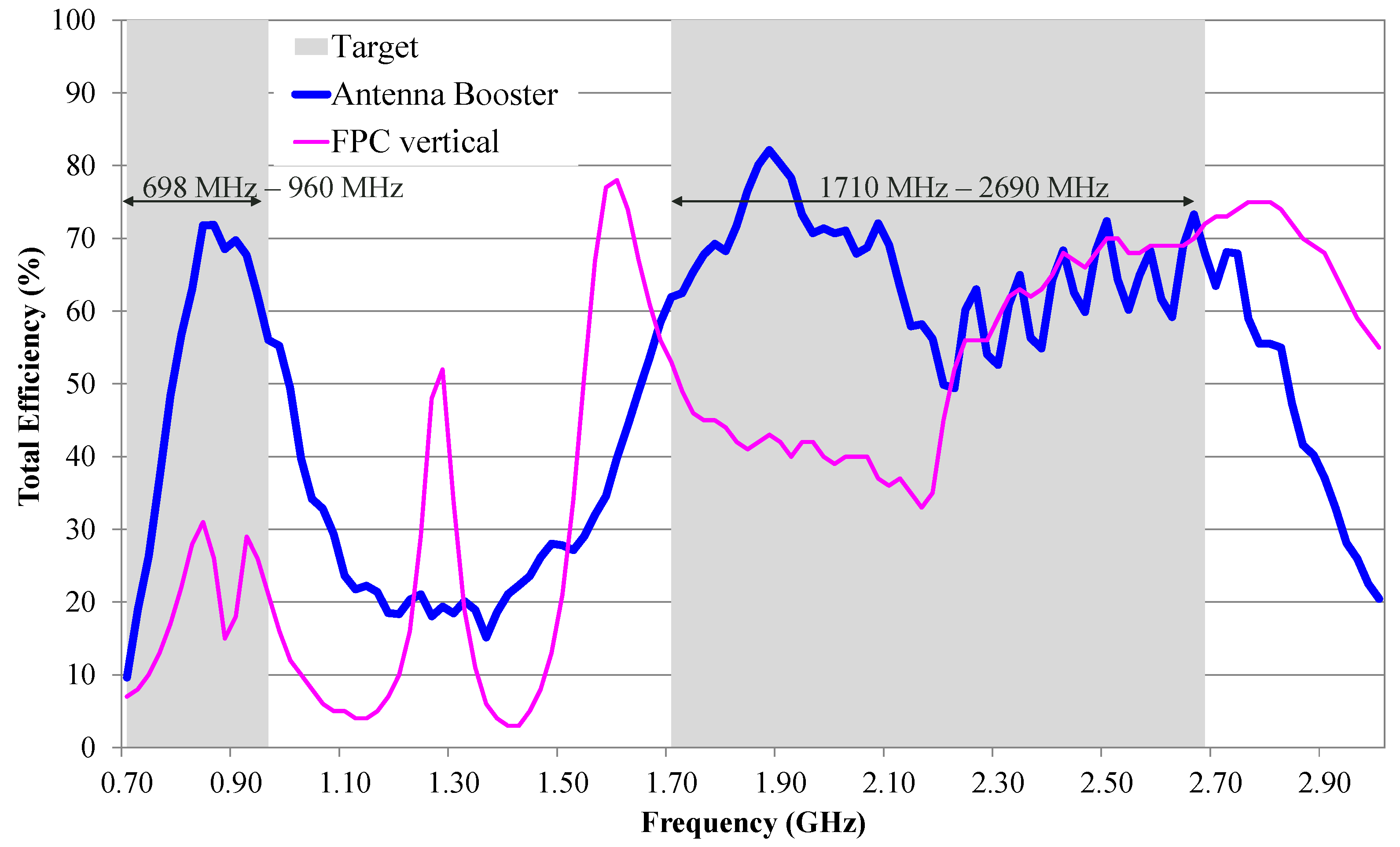
Finally, the FPC antenna is also analysed when it is vertically oriented on the same PCB (
Figure 6). Results in terms of total efficiency again reflect the worst performance more accused in the low-frequency region, where the difference between measured average total efficiency is 4.3 dB more for the antenna booster solution (
Figure 7,
Table 3).
Furthermore, not only the FPC antenna is again the worst in the vertical case, but it also forces the device to be at least 21 mm in height (the width of the FPC), which goes against the direction of designing thin IoT devices. On the contrary, the antenna booster solution is only 2.4 mm in height, enabling very thin IoT devices.
Next,
Section 3.2 and
Section 3.3 analyse two different PCB sizes representative of other IoT devices: a medium size of 95 mm × 42 mm and a small one of 65 mm × 42 mm.
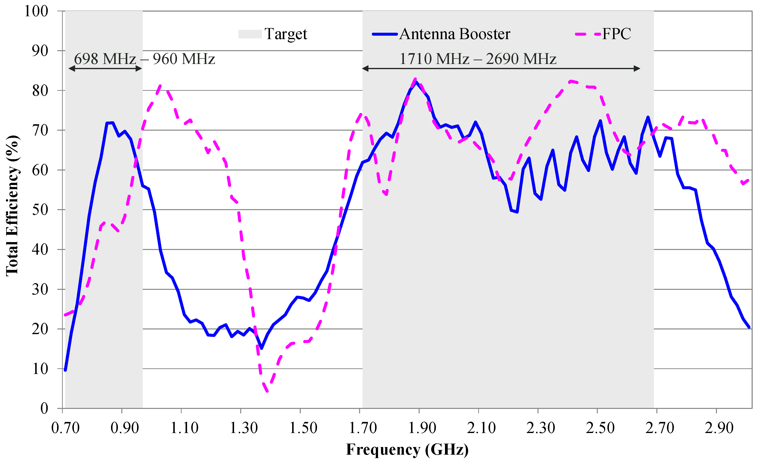
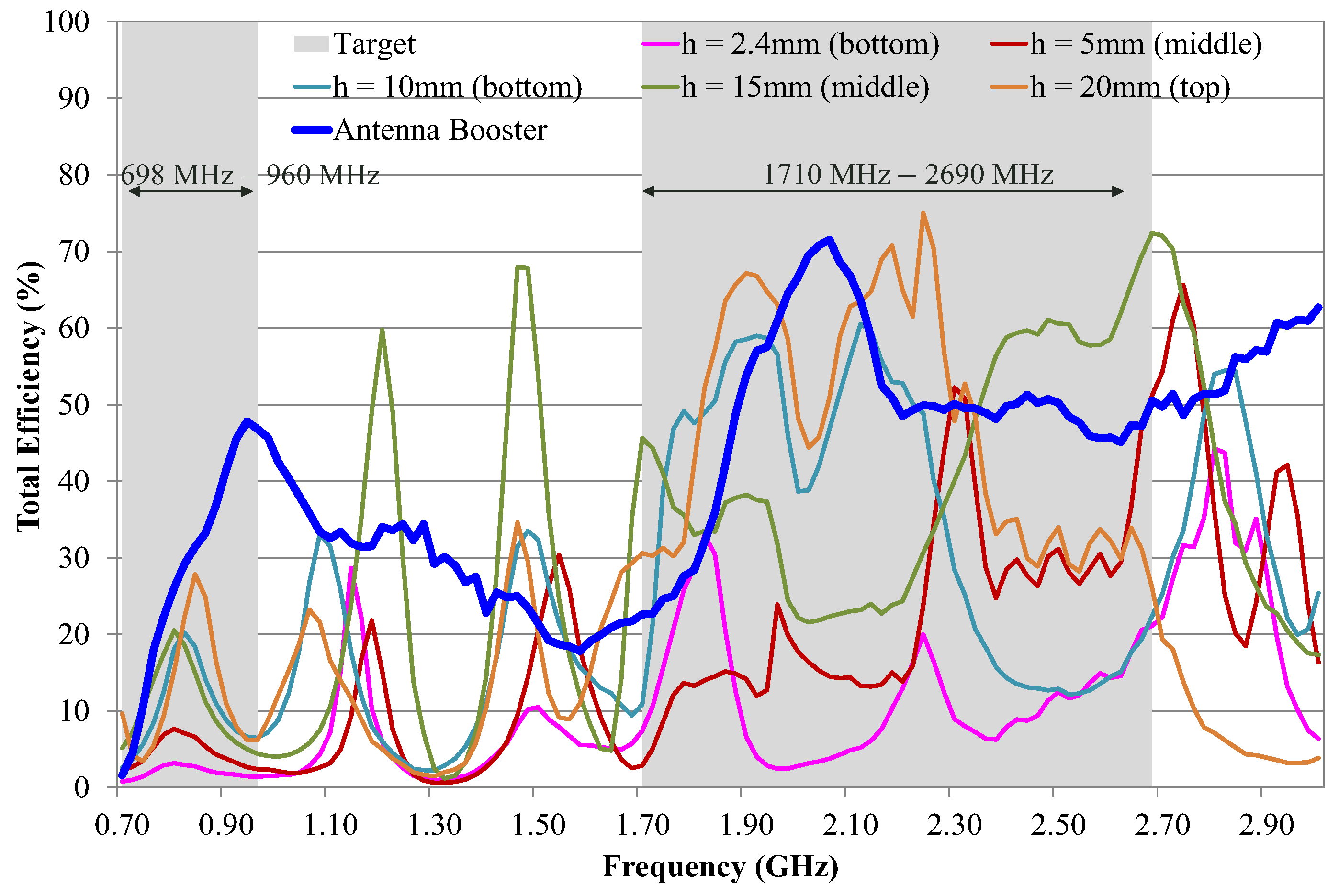
3.2. PCB 95 mm × 42 mm
This section compares the same antenna booster with the FPC antenna on a 95 mm × 42 mm PCB (
Figure 8). The matching network for the antenna booster is the same as the previous case.
As with the big PCB, for each height, three different positions of the FPC antennas are tested (top, middle, and bottom) (
Figure 9). The best result in terms of total efficiency is then selected (
Figure 10 and
Table 4). The antenna booster surpasses the FPC antenna in the low-frequency region (698–960 MHz). For example, for the FPC antenna at 2.4 mm height, which is the same as the antenna booster height, the measured total efficiency is only 2.8%. In contrast, it is 28.1% for the antenna booster representing 10 dB of more efficiency. Even for the height of 20 mm, the total efficiency is still lower than the antenna booster being 12.1% for the FPC antenna. In this case, the antenna booster is 3.6 dB more efficient. The antenna booster again outperforms in the high-frequency region (1710–2690 MHz). The FPC antenna must be placed at 20 mm to achieve a similar efficiency to the antenna booster. These results show again that not only efficiency of the antenna booster is much above the FPC antenna but also, to achieve compact IoT solutions, the antenna booster is preferred.
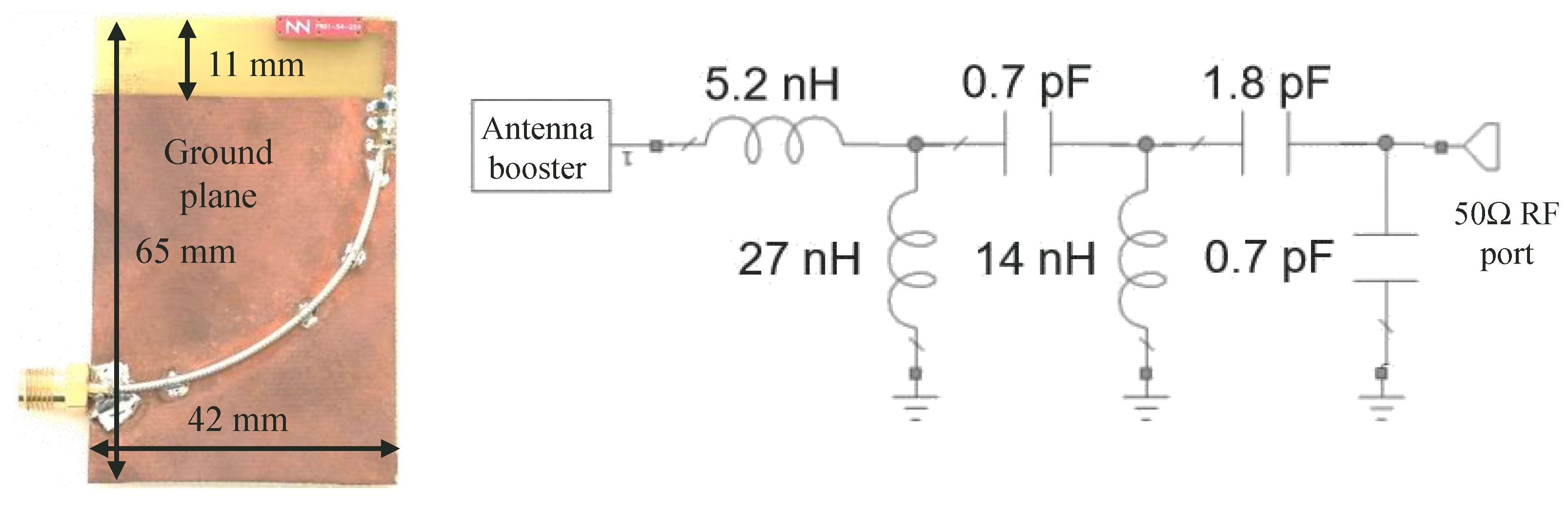
3.3. PCB 65 mm × 42 mm
This section compares the same antenna booster with the FPC antenna on a smaller PCB of 65 mm × 42 mm (
Figure 11). The matching network has been now optimised. This reflects the flexibility of the antenna booster technology since the same antenna booster can be used across all PCBs, and the only part that must be changed is the design of the matching network. Moreover, the matching network design is easy and faster than designing a new antenna from scratch [
11,
12].
As proceeded in the previous sections, the antenna booster is compared to the FPC antenna for 2.4 mm, 5 mm, 10 mm, 15 mm, and 20 mm heights. For each height, three different locations are analysed (top, middle, and bottom) (
Figure 12). Then, the best result in terms of efficiency is selected and compared with the antenna booster (
Figure 13,
Table 5).
The same trends are obtained for this small PCB: the total efficiency of the antenna booster is always better at both frequency regions. The antenna booster is 15.3 dB more efficient at the low-frequency region for the same height as the antenna booster. Even for the 20 mm height of the FPC antenna, the antenna booster is 3.8 dB better in the low-frequency region. As far as the high-frequency region is concerned, the antenna booster provides superior total efficiency too.
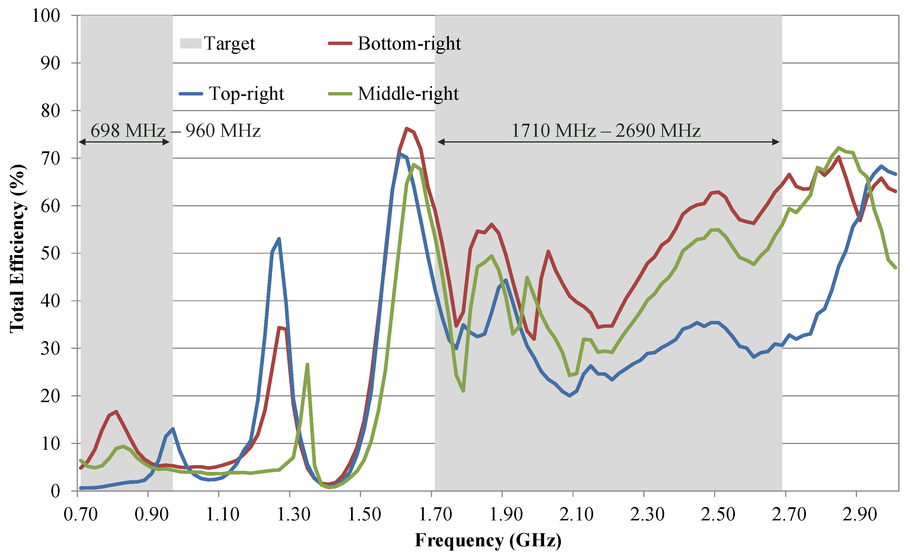
4. Dependence of the FPC Antenna Position on the PCB
Once the location is fixed on the PCB for the embedded antenna booster, no mounting instabilities impact the total efficiency performance since the antenna booster is an SMD component that can be automatically embedded on a PCB following a pick-and-place assembly process. This process can get accuracies down to 0.01 mm [
13]. However, the FPC antenna does not fit in a pick and place assembly procedure but on a human-dependent peel and stick process. In this regard, the total efficiency of the FPC antenna has been compared in three different positions: top, middle, and bottom (
Figure 4). For illustrative purposes, the sticker above 15 mm of the 130 mm × 60 mm PCB is discussed (
Figure 14). As clearly drawn from the results, the total efficiency is very dependent on the mounting process, which is not convenient since performance is not repetitive when building hundreds of thousands of IoT devices. For example, a variation in average of 4.2 dB in total efficiency is observed (
Table 6). Similar trends are found for the small and large PCBs.
At the frequency of 698 MHz of the low-frequency region, total efficiency can change from 6.4% at the middle of the PCB down to 0.6% at the top edge, representing a considerable variation of about 10 dB. At 2690 MHz, the performance also changes about 3 dB depending on the position of the FPC antenna.
5. Discussions
This paper shows that FPC antennas change their behaviour drastically from off-PCB conditions to on-PCB and are further impacted by the exact placing of the connecting transmission line. Since IoT devices are typically small and low-profile, the antenna in the majority of use cases should be embedded within the device. As mentioned, the size of FPC antennas for multiband operation from 698 MHz to 2690 MHz is such that it requires to be squeezed or folded into the casing of an IoT device resulting in unpredictable performance. Moreover, in smaller devices, the space available compared to the FPC antenna, which is 56 times larger in area (
Table 7) than the antenna booster, simply does not fit without folding. Additionally, antenna boosters are off-the-shelf SMD components easily embedded in a PCB. Once its position on the PCB is optimised (usually, the corner of the device provides the best bandwidth and efficiency [
14]), the performance remains predictable and stable when mass producing hundreds of thousands of devices. On the contrary, the FPC is more unpredictable since the position of the manually mounted FPC antenna impacts the performance, which may vary around 10dB, as discussed in
Table 6.
From a bill of material (BoM) perspective, the antenna booster technology needs an antenna booster and lumped SMD components for the multiband matching network. On the other hand, the FPC needs the FPC with an adhesive so the antenna can be attached to the casing of the device, a micro-coaxial line with a connector, and a receptacle on the PCB connecting the antenna. As a result, the price of an FPC antenna is approximately triple the price of an antenna booster, including the matching network components [
24].
Finally, the performance is always better for the antenna booster despite being eight times smaller concerning its maximum length (or 56 times less area) for all PCB sizes and even when the FPC antenna is 20 mm over the ground plane of the PCB. The vast differences are significant in the low-frequency region (698–960 MHz). For example, taking as a reference the FPC antenna at 10 mm over the ground plane, the antenna booster is 6.3 dB, 4.3 dB, and 7.6 dB more efficient on average at the low-frequency region for the small, medium, and large PCB, respectively. In the high-frequency region (1710–2690 MHz), the difference is not as severe, but still, the antenna booster exceeds the FPC antenna’s performance.
The poor efficiency performance of the FPC antenna on the ground plane is the result of a severe mismatching due to the proximity of the conductive antenna portion to the ground plane (
Figure 15). As an illustrative case, the S
11 for both technologies are compared considering the big 130 mm × 60 mm PCB. When the FPC is at the same 2.4 mm height as the height of the antenna booster, the S
11 at 900 MHz is only −0.61 dB which represents that only the 13.1% of the transceiver available power is delivered to the antenna. However, the S
11 at 900 MHz is −12 dB for the antenna booster, representing that 93.7% of the available power is delivered to the antenna. For the 10 mm and 20 mm height, S
11 is still very poor for the FPC antenna, being worse than −2 dB. At the high-frequency region (1.71–2.69 GHz), the S
11 for the FPC antenna is not worse than that in the low-frequency region but still presents deficient matching values compared to the antenna booster, which achieves an S
11 well below −6 dB across the whole 1.71–2.69 GHz frequency region.
The question is whether the performance can be again recovered by using a matching network. The matter is addressed by computing the potential bandwidth, which calculates the bandwidth an antenna system can reach with input impedance data. Potential bandwidth has been computed with Optenni-Lab [
15]. The issue is that the potential bandwidth of the FPC on-PCB decreases drastically, as expected from the basic antenna theory of antennas electrically close to conductive planes. The potential bandwidth is compared for the off-PCB and on-PCB for two frequencies (
Table 8). As shown, the potential bandwidth for the off-PCB is aligned with the required bandwidth at the low-frequency region (698–960 MHz = 31.6%) and the high-frequency region (1710–2690 MHz = 44.5%). However, for the on-PCB, the potential bandwidth is very poor (~1%) at both 900 MHz and 2200 MHz, meaning that bandwidth cannot be recovered even with the addition of a matching network.
As observed for both technologies, the ground plane impacts, especially in the low-frequency region. As the ground plane size increases, impedance bandwidth and total efficiency increase too. However, enlarging the ground plane beyond the 120 mm × 60 mm does not necessarily imply better results at the given frequency bands of operation. It has been shown that there is an optimum length of around 0.39λ to maximise bandwidth [
25] because the fundamental mode can be excited on the conductive portion of the ground plane.
6. Conclusions
Two technologies for IoT devices have been compared: antenna booster technology and FPC antennas. The off-PCB FPC antenna presents similar efficiency to the antenna booster. However, off-PCB is not the typical situation but on-PCB. In this scenario, the performance drastically deteriorates when placing the FPC antenna in the device.
The FPC antenna has been evaluated at several heights above the ground plane of a PCB from 2.4 mm up to 20 mm presenting in all cases worse efficiency values than the embedded booster antenna at both frequency regions 698–960 MHz and 1710–2690 MHz. When comparing the FPC antenna over the ground plane of the PCB at the same height (2.4 mm) as the antenna booster, total efficiency is 15.5 dB, 11.4 dB, and 18.1 dB more for the antenna booster at the low-frequency region for the small, medium, and large PCB, respectively. For the high-frequency region, the total efficiency is 4.8 dB, 6.2 dB, and 7.8 dB more for the antenna booster for the small, medium, and large PCB, respectively.
The FPC antenna also presents dependent behaviour on its position on the PCB, where total efficiency can change 10 dB. This situation is irrelevant for the embedded antenna booster since the position is fixed on the PCB and automatically mounted following a pick and place assembly process due to its SMD nature.
Based on these results, FPC antennas, like the one presented in this paper, are large, and when placed above the ground plane of the device, the efficiency drastically drops. A further negative impact on the overall FPC performance can be expected when batteries are placed in the device since they are covered with a conductive material and thus decrease the distance between the FPC and the conductive part of the battery. However, this falls outside the scope of this study. Additionally, the performance is unpredictable since it depends on the ability of the human being to mount the antenna on the PCB of the device. On the contrary, embedded antenna boosters are convenient for designing IoT devices due to their small size, multiband behaviour, off-the-shelf nature, cost competitiveness, and compatibility with the pick and place assembly process, ensuring stability when mass-producing devices with embedded antennas.
In summary, when leaving the antenna selection for IoT devices to the end of the design cycle, by just putting a UFL connector on the PCB in the initial design stages, the risks of not being able to get acceptable performance increase materially, and the design effort of selecting and tuning an antenna booster are easily recovered given the price difference and manufacturing cost savings.


