Article

Studies on the Chemical Etching and Corrosion Resistance of Ultrathin Laminated Alumina/Titania Coatings

by
Ivan Netšipailo
,
Lauri Aarik
,
Jekaterina Kozlova
,
Aivar Tarre
,
Maido Merisalu
,
Kaisa Aab
,
Hugo Mändar
,
Peeter Ritslaid
and
Väino Sammelselg
*
Institute of Physics, Faculty of Science and Technology, University of Tartu, W. Ostwald Str. 1, 50411 Tartu, Estonia
*
Author to whom correspondence should be addressed.
Corros. Mater. Degrad. 2025, 6(3), 36; https://doi.org/10.3390/cmd6030036 (registering DOI)
Submission received: 11 June 2025 / Revised: 15 July 2025 / Accepted: 25 July 2025 / Published: 2 August 2025

Abstract

We investigated the protective properties of ultrathin laminated coatings, comprising three pairs of Al2O3 and TiO2 sublayers with coating thicknesses < 150 nm, deposited on AISI 310 stainless steel (SS) and Si (100) substrates at 80–500 °C by atomic layer deposition. The coatings were chemically etched and subjected to corrosion, ultrasound, and thermal shock tests. The coating etching resistance efficiency (Re) was determined by measuring via XRF the change in the coating sublayer mass thickness after etching in hot 80% H2SO4. The maximum Re values of ≥98% for both alumina and titania sublayers were obtained for the laminates deposited at 250–400 °C on both substrates. In these coatings, the titania sublayers were crystalline. The lowest Re values of 15% and 50% for the alumina and titania sublayers, respectively, were measured for laminate grown at 80 °C on silicon. The coatings deposited at 160–200 °C demonstrated a delay in the increase of Re values, attributed to the changes in the titania sublayers before full crystallization. Coatings grown at higher temperatures were also more resistant to ultrasound and liquid nitrogen treatments. In contrast, coatings deposited at 125 °C on SS had better corrosion protection, as demonstrated via electrochemical impedance spectroscopy and a standard immersion test in FeCl3 solution.

1. Introduction

Stainless steel (SS) is an iron alloy containing at least 11% chromium, which helps prolong the lifetime of the material in corrosive environments [1]. AISI 310 is a type of SS used at high temperatures up to 1150 °C and is therefore widely used in industrial engineering plants. Its high chromium content (~25%) helps to form a natively adherent thin oxide layer enriched with chromia on the alloy surface to protect the steel against corrosion [2]. However, in environments with high humidity and the presence of corrosive agents, such as chlorine, the native oxide layer can be destroyed, leaving the surface prone to corrosion [3]. To protect the SS, thin-film coatings can be used to isolate the surface from an aggressive environment. Techniques such as magnetron sputtering [4,5]; spin-, dip-, or spray-coating [6]; and chemical [7,8] and physical vapor deposition [9] methods have been used to prepare protective coatings.
Atomic layer deposition (ALD) can produce pinhole-free conformal thin films [10]. The method is based on successive self-limiting surface reactions. Film growth occurs layer by layer, and the film thickness can be precisely controlled by controlling the number of growth cycles. Additionally, the coating properties can be tailored using two or more materials in the coating architecture, resulting in laminated or quasi-mixed structures. However, before using ALD to produce thin protective or functional coatings, ensuring that the coating can withstand the long-term use of the component or equipment in a specified environment is important.
In an earlier study of Matero et al., the authors suggested that, by combining the dense structure of Al2O3 and the chemical stability of TiO2 into a multilayer arrangement, the corrosion resistance of the coatings grown with ALD could be improved [11]. It is well known that Al2O3 is an amphoteric substance reacting with both acids and bases, acting as an acid with a base and a base with an acid. Contrary, TiO2 is insoluble in water, organic solvents, and inorganic acids and is slightly soluble in alkali, soluble in saturated potassium acid carbonate, and can be completely dissolved in concentrated sulfuric and hydrofluoric acids after boiling for a long time. However, the properties of ALD-grown thin films of alumina and titania may somewhat depend on the preparation parameters, as described below.
Shan et al. studied corrosion protection properties of ALD-grown titania thin films deposited from titanium tetraisopropoxide and water at 150 °C on stainless steel substrates [12]. Using electrochemical analysis methods, the authors found that the use of the coating significantly improves corrosion protection, but unfortunately, they did not carry out any long-term corrosion tests. Abdulagatov et al. showed that an Al2O3 ALD film grown from trimethylaluminum (TMA) and water at 120 °C alone was insufficient to prevent copper corrosion because of the dissolution of the film in water [13]. Also, TiO2 ALD film deposited on copper at the same temperature, using TiCl4 and water as the precursors, did not prevent the water corrosion of copper. Only an ultrathin alumina layer covered with a titania layer successfully protected the Cu substrate. Correa et al. demonstrated that alumina samples were found to be unstable in pure water, acid, and basic environments in the as-synthesized state (ALD at 150 °C) and after 450 °C thermal treatment [14]. The stability of alumina films in acidic and basic solutions was greatly enhanced after annealing at 900 °C. Titania films were found to be stable in acid after annealing at ≥450 °C. The authors also showed that the lowest porosity of the 50-nm-thick films has an Al2O3 ALD film, followed by ZrO2 and TiO2 films.
Marin et al. demonstrated that Al2O3 and TiO2 nanolaminates with two and four bilayers provided better corrosion protection to the AZ-31 magnesium alloy than a single layer of alumina or titania [15]. They also speculated that the improved defect sealing exhibited by the chemically alternating multilayer configurations could be explained by the different reactions between TMA and TiCl4 with the substrate. This can lead to better oxide nucleation on the defects during the first ALD cycles, thereby improving the overall quality of the protective coating. The successful use of similar Al2O3/TiO2 ALD nanolaminates for the protection of Al alloys was demonstrated in our previous studies [16], and the protection of different steels can be found in other studies by Marin et al. [17,18]. Another ALD nanolaminate Al2O3/Ta2O5 was used by Härkonen et al. for corrosion protection of hardened and tempered low-alloy carbon steel (AISI 52100 and 100Cr6), using a low-temperature deposition process with growth temperature, TG = 160 °C [19]. The best corrosion protection properties were observed for the thickest 120-nm coating: 3 × (20 nm Al2O3 + 20 nm Ta2O5) nanolaminate. However, it barely withstood a 4-h neutral salt spray test carried out according to ISO9227 standard [20].
Kong et al. showed that an ALD-grown TiN layer, which was followed by a PVD-grown CrN layer, oxidized in air and turns partly to TiOxN1−x, so that a double layer of TiOxN1−x-TiN was formed, which effectively sealed the CrN layer [21].
There have also been successful attempts to grow mixed AlxTiyOz thin films, but the aim of these studies was to use them as high-k dielectric films [22,23,24,25]. Härkönen et al. employed the salt spray test to demonstrate that an AlxTayOz thin-film mixture coating deposited on steel had much better durability than a single layer of any of these materials [26].
Corrosion protection properties of different metal oxide and silicon oxide ALD films have been studied by many scientific groups. Daubert et al. studied corrosion protection properties of ultrathin films (~50 nm) of Al2O3, TiO2, ZnO, HfO2, and ZrO2 that were deposited on copper metal using ALD, which corrosion protection was studied by using electrochemical impedance spectroscopy and linear sweep voltammetry methods [27]. The authors showed that the films of Al2O3 or HfO2 provided the highest level of initial corrosion protection, but films of HfO2 exhibited the best coating quality after extended exposure. Recently, Li et al. studied the corrosion protection of 1060 Al alloy (99.6% aluminum) with ultrathin Al2O3, TiO2, SiO2, and ZnO films and Al2O3/TiO2 laminate prepared with thermal ALD, excluding SiO2 film, which was grown with plasma-enhanced ALD, all at 110 °C [28]. Although the substrate material used (1060 Al alloy) is not prone to severe corrosion like the 2000 series Al alloys, though it contained insignificant quantities of Cu impurity, the best corrosion protection was achieved by using Al2O3/TiO2 laminate. Santinacci’s recent review of the usefulness of the ALD method in corrosion protection describes the principle of the ALD method; reviews both early and recent research on the application of the ALD method in corrosion protection; and focuses on the use of different materials (Al2O3, TiO2, Ta2O5, SiO2, ZnO, HfO2, ZrO2, Fe2O3, and Nb2O5 layers and TiO2/Al2O3 and Al2O3/Ta2O5 laminates) in protective coatings, as well as the use of different coatings in specific areas [29].
Many fields require using steel parts in acidic environments, such as the chemical or food industry, and modern energetics. Although SSs, including AISI 310, can withstand dilute acid solutions well, they require protection in more aggressive environments such as those with concentrated acids. However, the chemical resistance of metal oxide thin films deposited using ALD in wet aggressive environments has rarely been studied. Correa et al. studied chemical stability in neutral, acidic, and basic solutions of single thin films of alumina and titania, grown at TG = 150 °C and annealed at 450 and 900 °C in N2 atmosphere [14]. They demonstrated that alumina samples annealed at 900 °C were stable in 1-M H2SO4 and KOH solutions, but as-grown titania was found to be unstable in 1 M H2SO4, HCl, and HNO3 solutions, while titania annealed at 900 °C was unstable in a 1 M KOH solution. In our previous study, we examined the chemical resistance of different metal oxides, including titania and alumina films, grown on Si substrates using ALD from different precursors and at different temperatures (80–900 °C) after etching in hot concentrated sulfuric acid [30,31]. These studies required a relatively short etching time and revealed better resistance of the oxide films grown at higher temperatures. Additionally, our study demonstrated the higher chemical resistance of polycrystalline TiO2 than that of amorphous Al2O3. In the latest study, where the water precursor was replaced by ozone, we showed that, for TiO2 films, the etch rate appeared to be lowest for the films with the most developed preferential [0 0 1] orientation. The chemical resistance of the alumina/titania laminates was mainly determined by the resistance of the titania sublayers.
In this study, we describe the analysis results of alumina and titania nanolaminates deposited on steel and silicon substrates. The nanolaminated thin films were deposited over a wide TG range, allowing a comparison of the chemical resistances of the nanolaminates and monolayers that we studied earlier. Additionally, we analyzed and tested laminates via standard corrosion procedures in a salt solution, an ultrasonic bath, and liquid nitrogen. This allowed us to obtain comprehensive information on the chemical resistance, corrosion protection, and mechanical properties of the laminates prepared at the same TG, varying over a wide range, for better use as protective coatings in different applications.

2. Materials and Methods

2.1. Deposition of Thin Films

Nanolaminates were deposited on the surfaces of Si (100) and AISI 310 SSs (Goodfellow Cambridge Ltd., Hamburg, Germany; Fe/Cr25/Ni20) using laboratory-made flow-type [32] and R200 (Picosun OY, Espoo, Finland) ALD reactors. The AISI 310 samples were mechanically cut from a 2-mm-thick grinded sheet into 10 × 10 and to 40 × 40 mm2 squares and sequentially cleaned in an ultrasonic bath with toluene, acetone, and isopropyl alcohol (isopropanol, 99.5%; Sigma-Aldrich, Taufkirchen, Germany) for 5 min each, as in our previous study. After that, the substrates were treated for 5 min with a solution of acids heated to 70 °C: H3PO4 (85%, Sigma-Aldrich, Taufkirchen, Germany), HNO3 (65%, Sigma-Aldrich, Taufkirchen, Germany), HCl (37%, Sigma-Aldrich, Taufkirchen, Germany), H2SO4 (95%, Sigma-Aldrich, Taufkirchen, Germany), and H2O at a volume ratio of 15:2:5:5:73, followed by rinsing with distilled water and blowing them dry in a N2 stream [31]. Since AISI 310 contains 25% Cr, the surface of the alloy after the treatment was covered with a passive oxide layer containing mainly chromium and iron oxides, since nickel, although present in the alloy at 20%, does not oxidase in air at room temperature [33]. Highly polished Si (100) substrates were cleaned by boiling in a 5:2 mixture of concentrated H2SO4 (95%, Sigma-Aldrich, Taufkirchen, Germany) and 20% H2O2 (diluted from 38%, Sigma-Aldrich, Taufkirchen, Germany), followed by rinsing in deionized water, etching the native oxide in HF (37%, Sigma-Aldrich, Taufkirchen, Germany), and a final rinse in deionized water, covering the substrate with a nanometric oxide layer [30]. Al2O3 and TiO2 nanolaminates were deposited using the TMA (98%, StremChemicals, Bischheim, France) and H2O precursors and TiCl4 (99.9%, Sigma-Aldrich, Taufkirchen, Germany) and H2O, respectively. The precursors were maintained at room temperature. The H2O vapors used as the oxygen precursors were generated from deionized water. Nitrogen of 99.999% purity (AS Linde Gas, Tallinn, Estonia) was applied as a carrier and purge gas. The pressure of the flow-type ALD reactor chamber maintained at 220 Pa. The cycle times used for the deposition of TiO2 and Al2O3 were 2 s for TiCl4 or 3 s for TMA, 2 s for purging, 2 s for H2O, and 5 s for additional purging. To form the laminated structure at TG = 80–200 °C, the first 200 ALD cycles of TMA-H2O were deposited, followed by 200 ALD cycles of TiCl4-H2O, all repeated three times. For higher deposition temperatures (TG = 250–500 °C), the number of ALD cycles was increased to obtain a coating thickness between 90 and 150 nm. Similarly, the ALD parameters of the R200 reactor were adjusted and controlled via scanning electron microscopy (SEM) study of a cross-section of deposited coatings on Si substrates to obtain coatings with the same structure and thickness.

2.2. Etching and Characterization of Thin Films

Etching was performed stepwise, as in our previous study [30], in an 80% aqueous solution of H2SO4 (95–97%; Sigma-Aldrich, Taufkirchen, Germany) at 110 °C at varying step durations of 30–150 s, depending on the evaluated etching rate. Before etching, thin-film structures were cleaned with radio frequency plasma using Femto-1 plasma equipment (Diener Electronic GmbH & Co. KG, Ebhausen, Germany) with a gas mixture of 20% O2 + 80% Ar (AS Linde Gas, Tallinn, Estonia) for 300 s. Before and after each chemical etching step, the samples were rinsed with deionized water and dried in a N2 stream, and their coating thickness change was determined with a precise X-ray fluorescence (XRF) analyzer ZSX400 (Rigaku, Osaka, Japan) equipped with a wavelength dispersive X-ray spectrometer that had six analyzing crystals. From the XRF measurement data, the mass thicknesses of both the titania and alumina sublayers were calculated using a thin-film analysis program (Rigaku, Osaka, Japan), considering the known laminate structure and substrate composition. The coating mass thickness was obtained by summing the mass thicknesses of the sublayers. The physical thickness of the film was determined in two ways, firstly on the basis of the mass thicknesses of the sublayers using the densities of the film materials determined by the X-ray reflection method on similar films. Secondly, the thickness of some coatings was measured directly by SEM on a cross-section of the coating, the SEM having been pre-calibrated with a special calibration sample. The same thin-film program was used to perform quantitative elemental analysis of thin films with the XRF method. Two calibrated samples were used to evaluate the level of analytical uncertainty of the method. The first calibration sample has a 200 ± 5-nm-thick sputtered titanium layer on the Si substrate, and the second a 52 ± 5-nm-thick TiO2 ALD film grown at 110 °C on the Si substrate. The latter film contained 5.7 mass% chlorine; the content was determined via electron probe microanalysis (EPMA) using a cleaved NaCl monocrystal as the standard and a special thin-film program, STRATAGEM (SAMx, Trappes, France) [34].
The etching rates ke = ke (TG) for a laminate grown at a certain temperature on a specific substrate were determined separately for the titania and alumina sublayers. For a sublayer, the ke is calculated as follows:
k e   =   ( d 0     d t ) / t ,
where d0 is the total thickness of the sublayer before etching, and dt is the total thickness after an etching time interval t, as shown in Figure 1.
The relative etching rate of a sublayer was determined as
k e , r e l ( T G ) = k e ( T G ) / k e , m a x ,
where ke,max is the maximum etching rate of the laminate. The latter variable was used to characterize the etching rate of an infinitely thin coating deposited at a given temperature, which produced coatings with the maximum etching rate; in our case, at 80 °C. Based on the etching rate data obtained in this study, and that given in our previous study [30], we define ke,max = 1.1 nm/s for both alumina and titania sublayers. The etching resistance efficiency Re (%) of a coating prepared using TG is defined as
R e ( T G ) = ( 1 k e , r e l ( T G ) ) × 100 .
To obtain the TiO2 sublayer phase composition, all samples were analyzed by grazing incidence X-ray diffraction (GIXRD) before etching using a SmartLab (Rigaku, Osaka, Japan) diffractometer. The diffractometer has a Parallel Slit Analyzer ensuring parallel beam (PB) geometry and was equipped with an X-ray tube with a rotating Cu anode operating at 8.1 kW. A grazing angle of 0.30 ± 0.02° was used for measurements. The structure of the titanium phase was also studied by SEM and Raman spectrometry using an inVia (Renishaw, Gloucestershire, United Kingdom) spectrometer–microscope system with a 514.5-nm laser. Surface morphologies of the coatings were studied using a high-resolution SEM (HR-SEM; Helios NanoLab 600, FEI Company, Hillsboro, OR, United States of America (USA)). Cross-sections of the coated structures were prepared using a focused ion beam (FIB) system of the same SEM. Ultrathin lamellae of the nanolaminates were also prepared by FIB and first examined by HR-SEM in the scanning transmission electron microscope (STEM) mode. Furthermore, the lamellae were analyzed using a Titan 200 (FEI Company, Hillsboro, OR, USA) high-resolution transmission (scanning) electron microscope (HR-(S)TEM), allowing the exploration of both transmission electron microscopy and scanning transmission microscopy modes with an 80–200 kV electron beam.

2.3. Testing of the Coatings

Corrosion tests were performed using a three-electrode electrochemical cell PTC1 (Camry Instruments, Warminster, PA, USA), with a saturated calomel electrode (SCE) and a Pt wire as the reference and counter electrode, respectively. Additionally, a steel sample with and without ALD coating was used as the working electrode. The tests were performed using a potentiostat–galvanostat Reference 600 (Gamry Instruments, Warminster, PA, USA), and the samples were placed in a 0.5 M NaCl solution at room temperature. All potentials reported in this study were measured versus SCE. The testing area of the studying electrode was fixed at 1.0 cm2 using special 3M™ electroplating tape masks (Gamry, Warminster, PA, USA). Linear sweep voltammetry (LSV) measurements were performed after stabilizing the open-circuit potential (OCP) for 30 min, followed by the scanning potential in the anodic direction at a rate of 1 mV/s, starting from approximately 200 mV below the OCP in the cathodic region. Electrochemical impedance spectrometry (EIS) measurements were carried out after 30 min of stabilization/immersion and 24 h of immersion in the electrolyte in the frequency range of 10−2–10−6 Hz with an AC perturbation amplitude of 10 mV (RMS), using the same potentiostat. Fitting of the spectra was done using Gamry software, in which depressed capacitive loops are treated as constant phase elements (CPE) [35], which impedance is given by ZCPE [36]:
Z C P E   =   1 / [ ( i · ω ) n · Q ] ,
where i is the imaginary unit, ω is the angular frequency (ω = 2π f, f being the frequency), and n and Q are explained below.
It is assumed that the microroughness and heterogeneity of the surface generates a nonuniform distribution of the charge, which results in a dispersion of the time constants:
τ   =   R · C ,
where R is resistance, and C is capacitance, responding at different frequencies. With this interpretation, Q is the frequency-independent component and is proportional to the area of the active sites that contribute to the process, whereas the exponent n indicates the deviation from an ideal dielectric behavior, with n = 1 for an ideal capacitor and n = 0 for an ideal resistor [36].
Immersion tests were carried out in accordance with the ASTM G48A standard [37] in 6% FeCl3 solution at 50 °C, using a Thermostatic Lab Water Bath (JOAN LAB Equipment Company, Huzhou, China). The samples were placed vertically in laboratory glassware. After 24, 48, and 72 h of immersion, the samples were removed from the beakers, rinsed with deionized water, blow-dried, and photographed.
Ultrasonic tests of the coated structures were performed at room temperature in an ultrasonic bath (Metason 1600, Struers Scientific Instruments, Copenhagen, Denmark) filled with deionized water and operating at a power of 80 W for 10 and 30 min.
Temperature shock tests were performed in an open Dewar vessel filled with liquid N2 during the test period of 20 s. Subsequently, the samples were warmed to room temperature and dried under a stream of N2.
Generative artificial intelligence (GenAI) was not used in this work.

3. Results

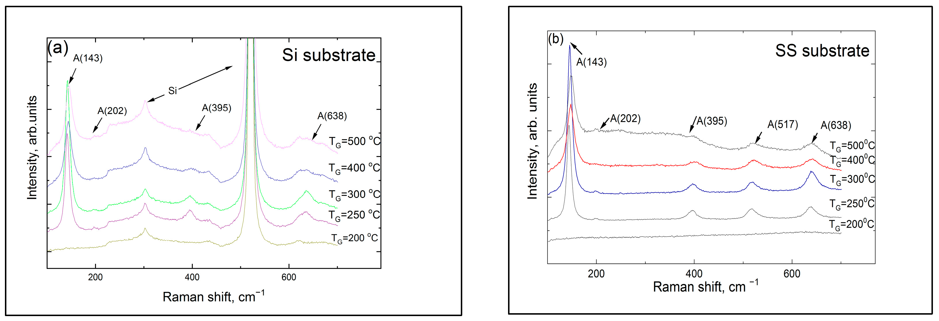
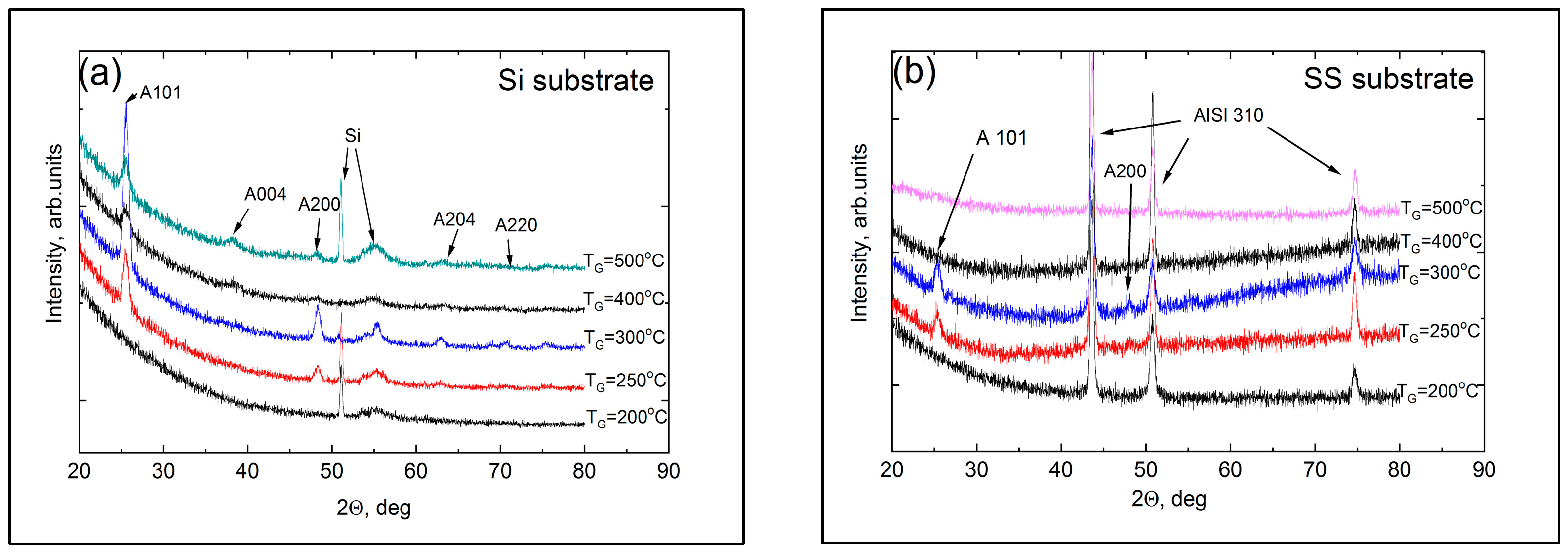
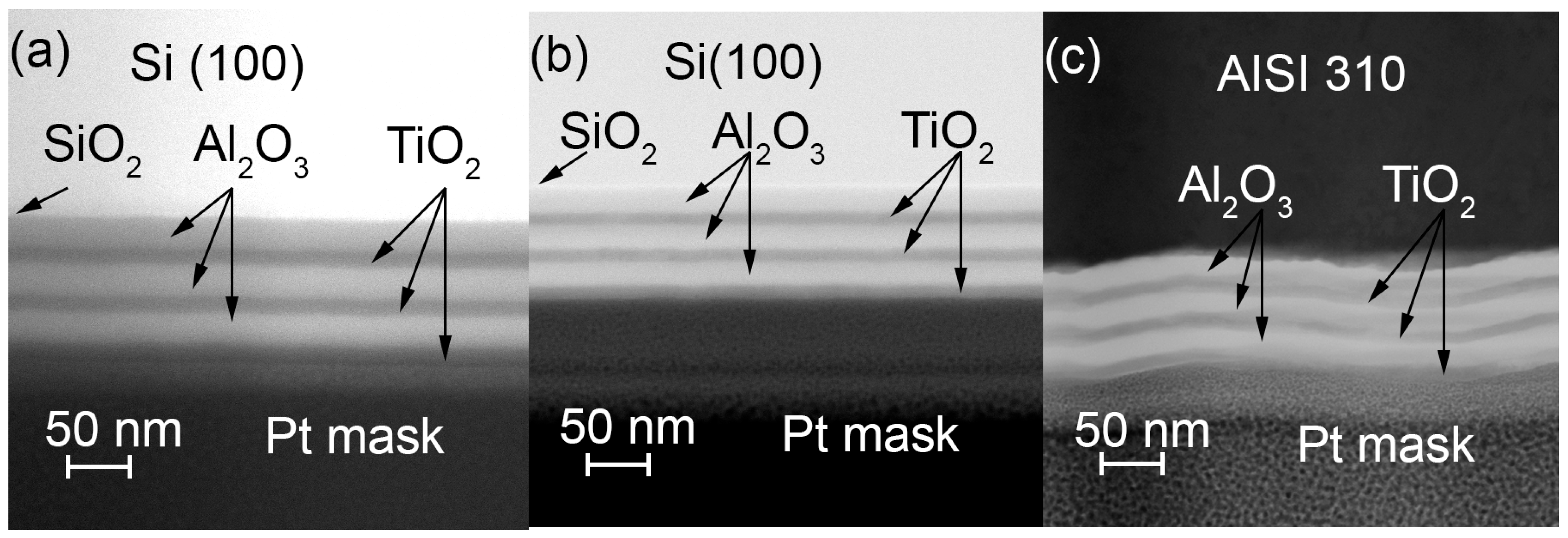
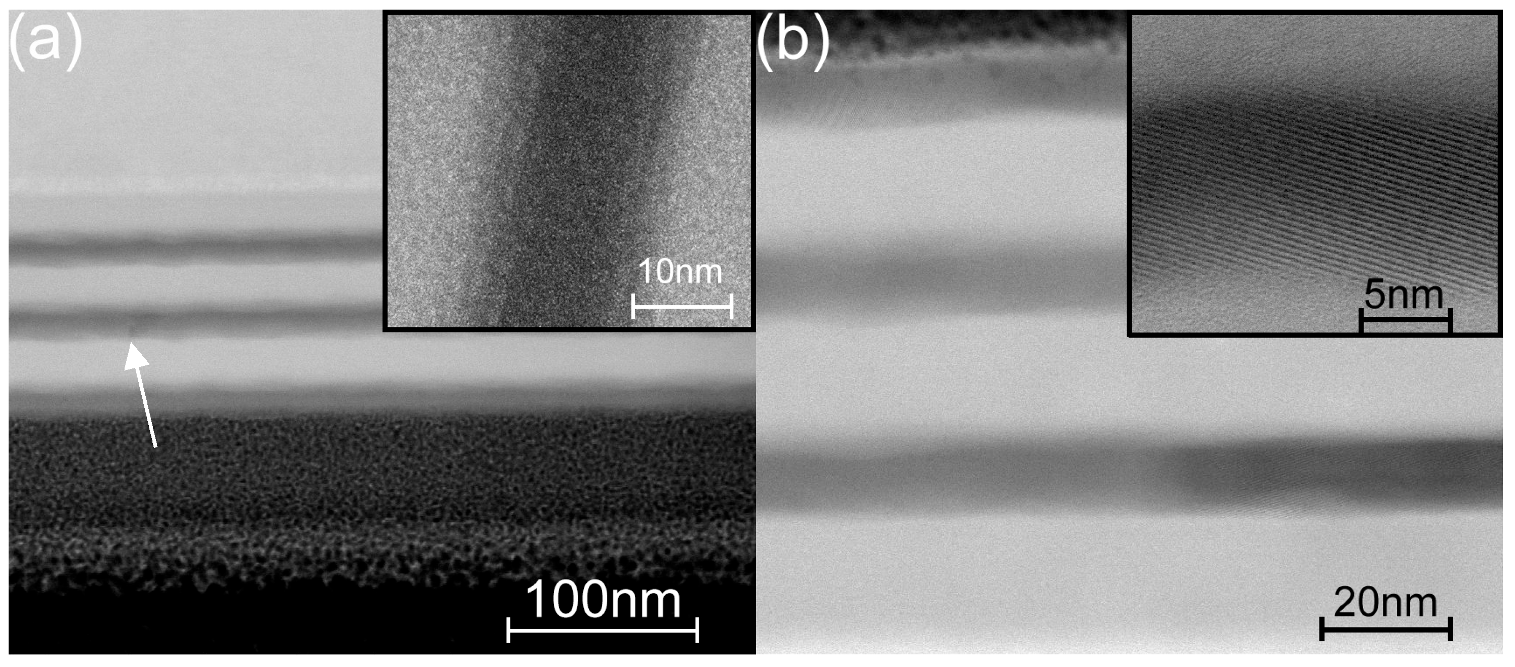
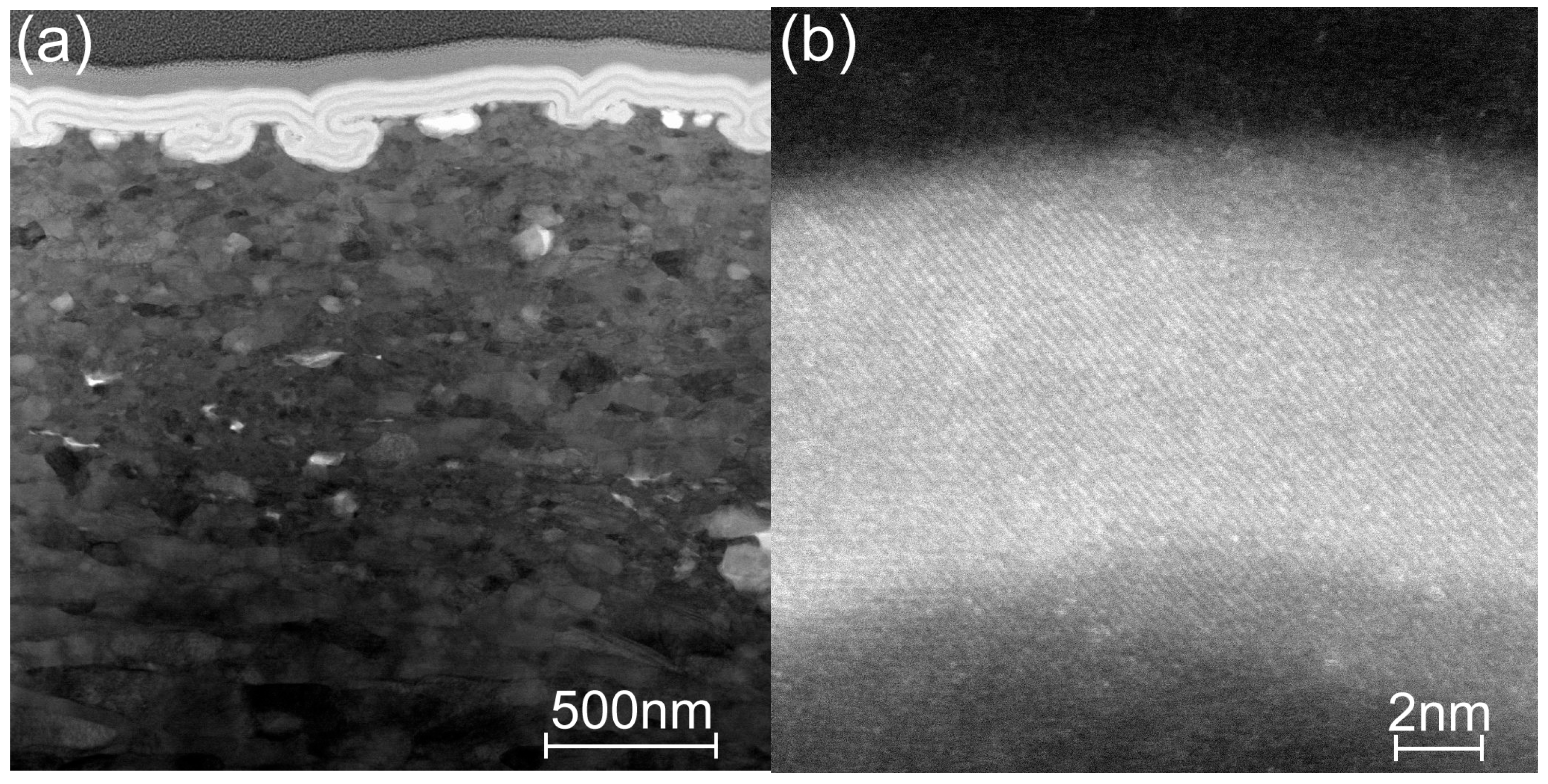
3.1. Structure, Composition, and Morphology of the Coatings

According to the Raman measurements, the titania coating sublayers deposited on Si and SS substrates were amorphous at TG ≤ 200 °C (Figure 2). The strongest band at 143 cm−1 belonged to the anatase phase that appeared at TG = 250 °C.
GIXRD measurements were performed to determine the presence of the anatase and rutile phases in the titania sublayers of the laminated coatings; the diffraction patterns are shown in Figure 3.
The patterns confirmed that titania crystallization began at TG = 250 °C in the coatings on both substrates, and a pronounced anatase phase formed at 300 °C. However, the presence of rutile was not registered even at 500 °C. Additionally, no peaks belonging to titanium oxide were detected when the films were deposited at TG ≥ 400 °C on SS. However, this does not imply that the titania sublayers do not contain any crystalline material, especially since the Raman spectra in Figure 2 showed the presence of an anatase phase in the titania sublayers in coatings deposited on both Si and SS substrates. One reason why the anatase peaks are not seen in GIXRD patterns of high-temperature coatings on SS substrates could be connected with the crystallite dimensions, which could be very small in the high-temperature coatings; this leads to strong broadening of the diffraction peaks and a reduction in their intensity. Although the intensities of the Raman bands depend on the crystallite dimensions as well, the effect is several times stronger for GIXRD. In a recent study, Raman spectra of TiO2 nanopowders were studied, and it was shown that, as the particle size changed from 5 to 30 nm (an increase of six times), the width of the anatase Raman Eg band, centered at 142.9 cm−1, changed from 8.9 to 11.7 cm−1 (or 1.3 times) [38]. It is well known that the width of the XRD peak is inversely proportional to the dimensions of the crystallites, so, for the same change in the dimensions of the crystallites, the XRD peak width would increase by a factor of six. Below, in Section 3.2, we show that the substrate influences the composition of the titanium oxide substrate at low TG, so that the chlorine content of the deposited coatings is somewhat lower for SS substrates than for Si substrates. Based on this effect, we suppose that crystallization at higher TG values may also affect the substrate material, so that the dimensions of the anatase crystals of the titania sublayer deposited at the same TG value are smaller in the coating on the SS substrate than in the coating on the Si substrate; this probably explains why no anatase diffraction peaks are seen in coatings grown on SS substrates at 400 and 500 °C. However, it is difficult to determine whether these coatings also exhibit a preferential orientation of anatase crystallites because of the low thickness of the titania sublayers and the low intensity of the GIXRD peaks.
The morphology of a bare ground SS substrate has typical defects, such as bumps, cavities, and grinding lines, as shown in Figure 4a. The surfaces coated at low temperatures have allocated areas/clusters that repeat the substrate topography, as shown in Figure 4b. The surfaces of the laminates deposited at higher temperatures have a globular topography, which is typical for ALD-coated metal surfaces [19].
The difference between cross-section images of the nanolaminates, grown on silicon at 160 and 300 °C, are presented in Figure 5a,b. The full coating and its sublayers are uniform, and the coating adheres well to the substrate surface. Figure 5c shows another cross-section image of a nanolaminate grown at 250 °C on a SS substrate. In this case, the laminate exhibits wavy morphology following the topography of the substrate. The sublayer transitions are somewhat blurred in the parts angled towards the plane of the cross-sectional image; however, in other parts, the transitions are sharp and clearly visible.

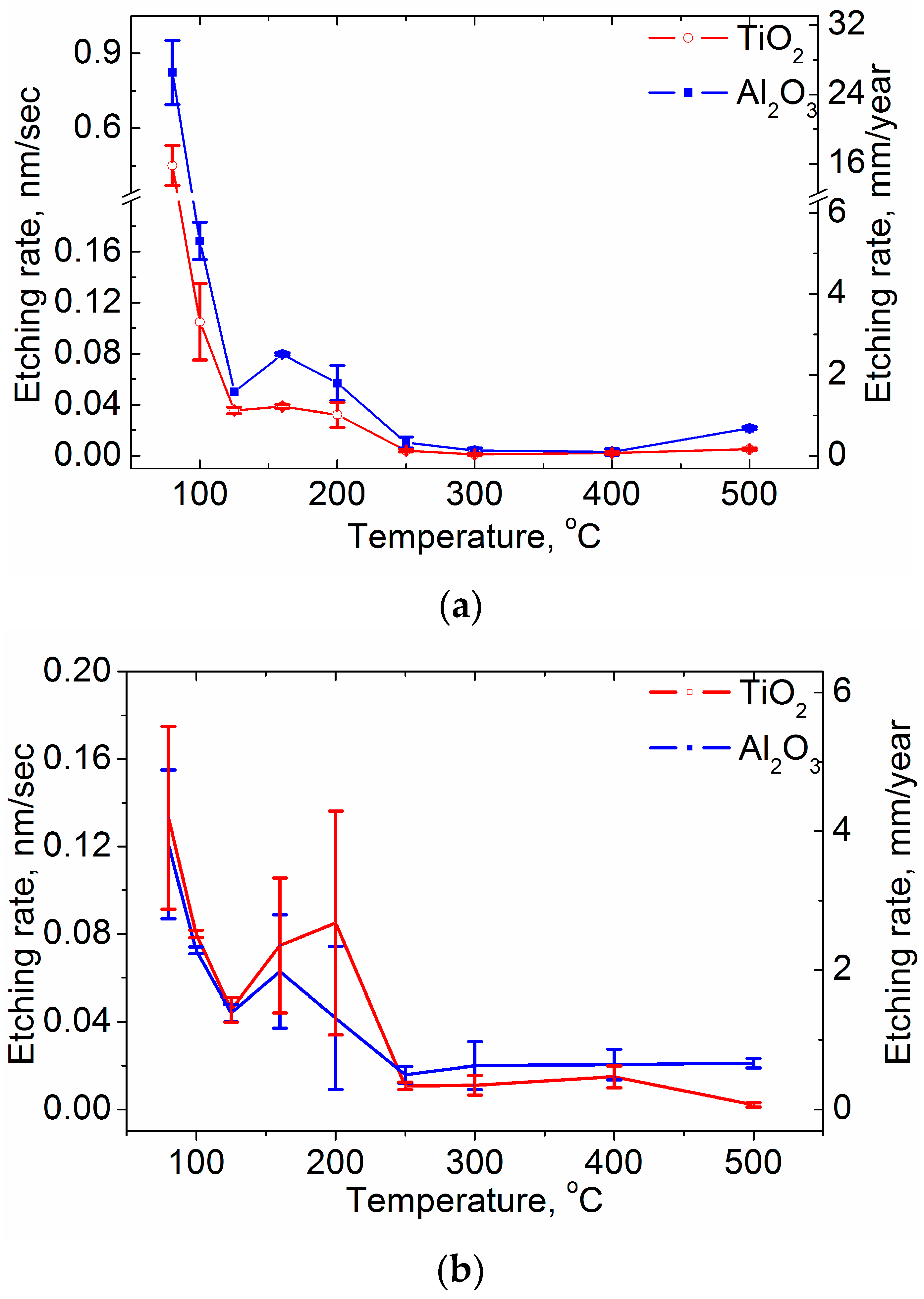
3.2. Chemical Etching Results of the Coatings

The dependence of Re on the TG of the laminates etched in hot H2SO4 solution is shown in Figure 6. Sample data and ke values are presented in Table 1 and Figure A1 in Appendix A. The data in Table 1 show that not all the coatings survive 10 min of etching; in some cases, using shorter time intervals is necessary to obtain sufficient measurement points while maintaining at least 50% of the original thickness of the coating (d0).
Analysis of the graphs in Figure 6 shows that the etching resistance efficiency of the coatings deposited at the same TG values slightly differs for different substrates. First, let us examine the coatings deposited on the silicon substrates (Figure 6a). The lowest Re values of 15% and 50% were obtained for the coatings prepared at TG = 80 °C for the alumina and titania sublayers, respectively. These values reached a plateau of ≥98% at TG ≥ 250 °C and had a small decrease for the alumina sublayers at TG = 500 °C, probably due to the initial decomposition of TMA at such a high temperature. However, at TG = 160–200 °C, the Re values somewhat decreased to ~93% and ~96% for the alumina and titania sublayers, respectively. In contrast, the coatings deposited on the SS substrates (Figure 6b) had higher Re ≈ 88% values at TG = 80 °C for both sublayers. Simultaneously, the Re decreased at TG = 160–200 °C and was slightly different at ~95% and ~93% for the alumina and titania sublayers, respectively. Additionally, a high level of Re ≈ 100% was reached only for the titania sublayers at TG = 500 °C, whereas, for the alumina sublayers, the high temperature plateau remained at Re ≈ 98%.
Thus, the etching protection efficiency of the coatings prepared at TG ≤ 100 °C is low, especially for the coatings deposited on the Si substrates. In our previous study, we showed with EPMA that titania films grown at 100 °C on Si substrates using TiCl4 and H2O precursors had a high content of residual impurities [39]. Later, using the Rutherford backscattered spectroscopy (RBS) and time-of-flight elastic recovery detection analysis (TOF-ERDA) methods to determine the chlorine and hydrogen contents, respectively, we showed that the titania film contained 3.0 and 1.7 at.% Cl and H, respectively [34]. In addition, we found that the content of both elements decreased significantly at higher deposition temperatures, e.g., for the titania layer grown at 300 °C, the impurity concentration was below the detection threshold of <0.1 at%. To check the hypothesis that the substrate could also significantly influence the ALD process of the laminate at a low TG range, we prepared laminate coatings on the Si and SS substrates in the same run at 100 and 125 °C and analyzed their composition via XRF. Table 2 presents the analyzed results.
XRF analysis showed that the ALD surface reactions on the AISI 310 substrate were more efficient than on Si (100), resulting in higher total mass thickness values of the coating and lower impurity contents in the films deposited on SS at TG = 100–125 °C. The chlorine concentration was 1.2 and 1.4 times lower for the films deposited at TG = 100 and 125 °C, respectively (Table 1).
Although the chlorine content decreased with the increasing TG, it remained higher in the coatings deposited on the Si substrates, and the ratio increased for the higher TG. Thus, the substrate type influences the ALD processes substantially. Furthermore, deposition at TG = 125 °C and a lower content of residual impurities can increase resistivity to chemical etching. Notably, in our previous study, we indirectly discovered that the crystallization of titania sublayers in the rutile phase was directly influenced by a monocrystalline sapphire substrate throughout a laminate with four chromia sublayers [40].

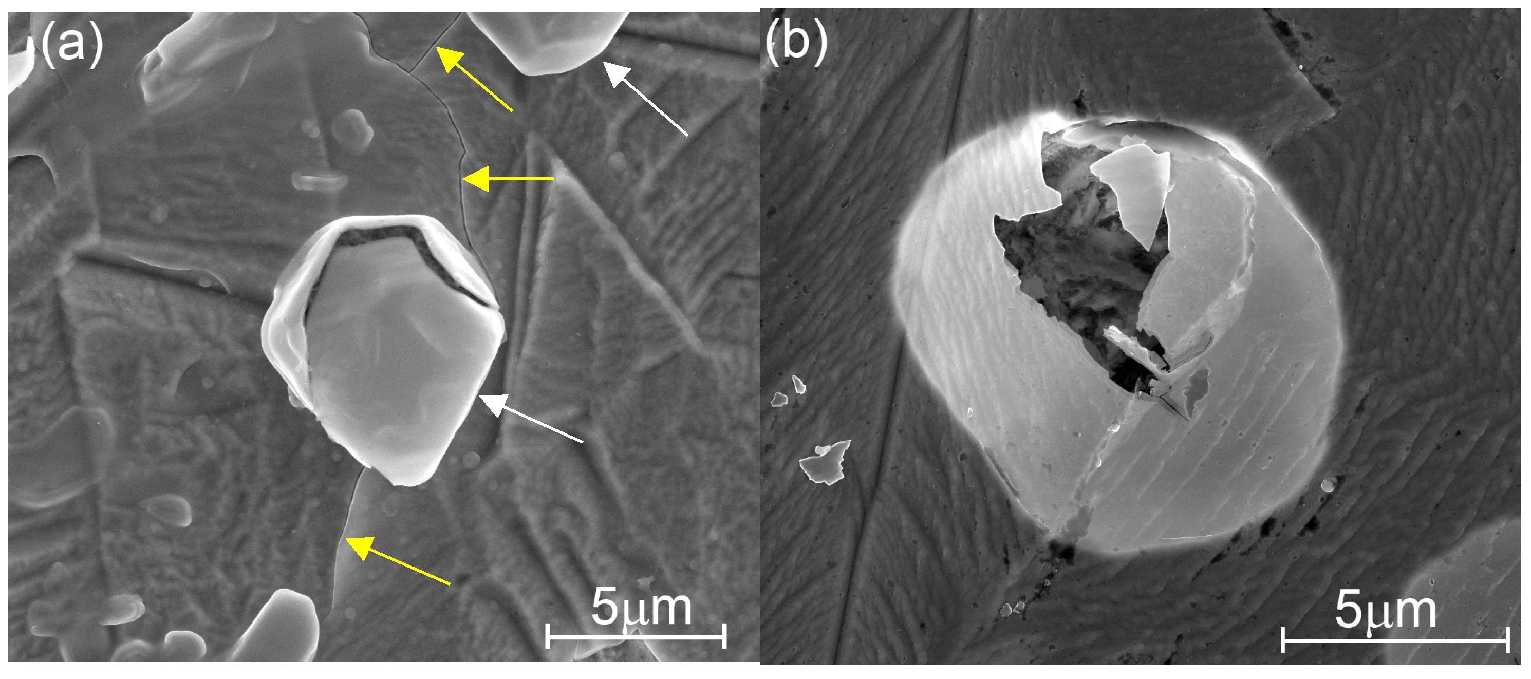
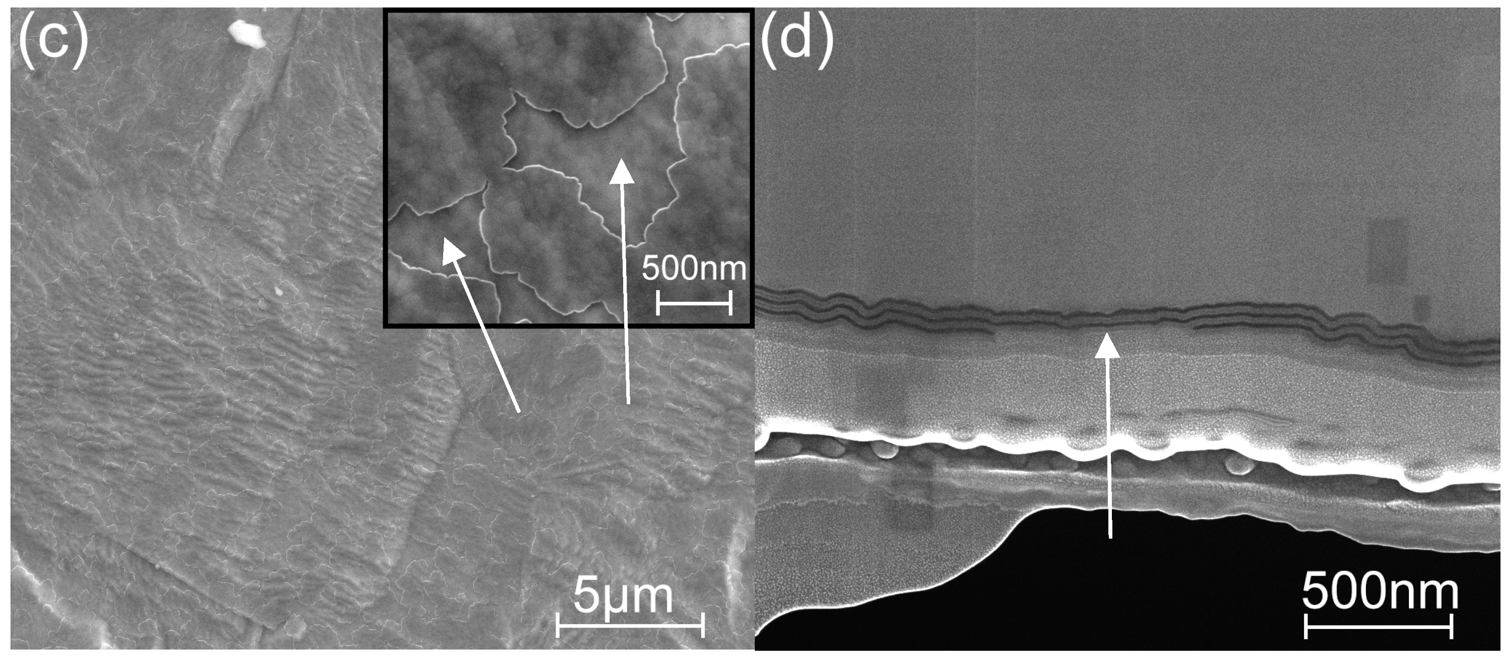
3.3. Microscopy Study of the Etched Coatings

To study the etching dynamics of the coatings and the process dependence on the deposition temperature, we investigated the surfaces and cross-sections of the etched structures using HR-SEM. These investigations revealed certain characteristics of the etching process, as shown in Figure 7, Figure 8 and Figure 9. Defect generation on low-temperature nanolaminate coatings after only a few minutes of etching is shown in Figure 7. At the beginning of the etching process, local nano-defects are created, which allow the acid droplets to penetrate the metal substrate; after a period of time, the protective cover develops a localized defect, probably due to gases generated by corrosion processes, and the coating is lifted locally, i.e., it is separated from the substrate and is probably going to crack. The defect resembles a broken blister, and this kind of coating destruction was observed mainly for the laminates grown at TG = 100–125 °C (Figure 7 and Figure S1).
Therefore, in Figure 7a and Figure S1a, several blisters, holes, and cracks can be seen, indicating the possibility of complete rapid destruction of the entire coating grown at TG = 100 °C with further etching. Similar holes were formed in the coatings deposited at TG = 125 °C during the etching process, but the proportion was smaller than that in the films deposited at a lower TG, and no cracks were detected after 5 min of etching (Figure 7b and Figure S1b). Therefore, the etching resistance efficiency of this coating was slightly higher (Figure 6b).
The graph in Figure 6b shows that the Re value of coatings applied to metal increases to 98% when the TG increases to 250 °C. Figure 8 shows SEM images of the coating surface and cross-section before etching (Figure 8a,b) and after 5 min of etching (Figure 8c,d). Both the surface and cross-section images of the etched structure show that the etching of the laminate partly removes the outermost sublayers (see the arrows in Figure 8c,d) while not instantly generating bubble holes throughout the coating, as is the case for the coatings deposited at TG ≤ 125 °C. However, increasing the etching time to over 10 min led to coating destruction due to the formation of blister-like defects (Figure S1c).
Further increasing the TG to 400 °C preserves the resistance to the etching of the coating, as shown in Figure 9, where a cross-section of the coating etched over 10 min shows partially preserved laminate sublayers still protecting the SS substrate.
The graphs in Figure 6 show a local decrease or persistence in the Re at TG = 160–200 °C, which is more pronounced on the coating deposited on SS than that on the Si substrate. This could be related to the start of the thin-film crystallization, as our previous studies have demonstrated the formation of crystallites of submicron dimensions starting at TG = 150 °C [30,41]. However, the thin films in those studies had thicknesses greater than 200 nm, but in this study, the thickness of the titania sublayers was only ~12 nm. Additionally, the titania sublayers were buried between the fully amorphous alumina sublayers in the laminates. Therefore, the GIXRD and Raman methods detected the anatase phase only in the laminates grown at TG ≥ 250 °C, as shown in Figure 2 and Figure 3, respectively. Nevertheless, we expected that titania nanocrystallites could be formed in the coatings grown at TG = 160–200 °C and that they could be too small to be discovered via Raman and XRD analyses but could still influence the etching rate of the layers by generating additional defects and/or structural inhomogeneity in the titania sublayers.
To better understand the structural development of the titania sublayers in the laminates grown at 160 and 200 °C, the lamellae of the coating cross-sections were prepared via FIB and examined using HR-SEM and HR-(S)TEM. SEM images in bright field STEM mode of the cross-sections of the laminates grown on the Si substrates at TG = 160 and 200 °C are given in Figure S2a,b, respectively. While all sublayers of the laminate grown at TG = 160 °C are amorphous, the titania sublayers in the laminate grown at TG = 200 °C have some distinctive nanocrystallites.
To obtain more detailed information on the structure of the titania sublayers in the laminate, an additional microscopic study was performed on a second set of samples prepared at intermediate temperatures (TG = 160–200 °C). In Figure 10a, a HR-SEM image shows an overview of the laminate (TG = 160 °C), and the inset shows a HR-TEM image of a titania sublayer of the same laminate. In the main image, small, darker areas in the titania sublayers can be observed (marked with an arrow), whereas, in the HR-TEM images, no clearly crystallized areas are evident. Simultaneously, both images show ~2-nm-wide blurred boundary regions between the sublayers inside the laminate, which are also visible in Figure S2a. These boundary regions cannot be induced by the roughness of the substrate, as the interfaces between the Si substrate and the thin SiO2 layer and between the latter and the first alumina layer are straight and narrow (Figure S2a). We assumed that the boundary regions could show some pre-crystallization inhomogeneity in the titania sublayers. Similar boundary surface irregularities between the titania and alumina sublayers in a laminate grown at 200 °C were reported in [42], where the authors referred to it as an interdiffusion layer (AlTiO) with an approximate thickness of 1.5 nm, although no study on the composition of this layer was presented. The blurred boundary regions also exist in the laminate deposited at 200 °C in this study, and the titania sublayers are partly crystallized (Figure 10b and Figure S2b), similar to the results given in [42]. The HR-TEM images of the laminate cross-section clearly show monocrystalline nanocrystals alternating with amorphous regions in the titania sublayer.
The cross-section of the laminate grown at 200 °C on the SS substrate is shown in Figure 11 and Figure S2c. As evident in the overview image in Figure 11a, the laminate covers all unevenness and pores on the metal surface. Additionally, the high-magnification image in Figure 11b shows that the titania sublayer is crystalline. Figure S2c shows the titania sublayer of the same laminate from a slightly shifted position, in which a nanocrystallite is embedded in the amorphous layer. Thus, the titania sublayers in the laminate grown on either the Si or SS substrate at 200 °C are partially crystallized. Further increasing of TG increases the crystallization levels of the titania sublayers (Figure S2d, TG = 300 °C), leading to development of a columnar structure of the anatase crystallites in the titania sublayer deposited at 400 °C (Figure S2e).
Overall, the inhomogeneity of the interfaces in the laminates grown at 160 °C and initial crystallization of titania in the laminates grown at TG = 200 °C, which leads to the coexisting of amorphous and anatase phases in the titania sublayers, are probably the reasons behind the slow increase in the etching resistance efficiency of the coatings prepared at these temperatures.
An overview of the coating preparation conditions, the crystallinity of the titania sublayers, and the etching data of the coatings is given in Table 1.

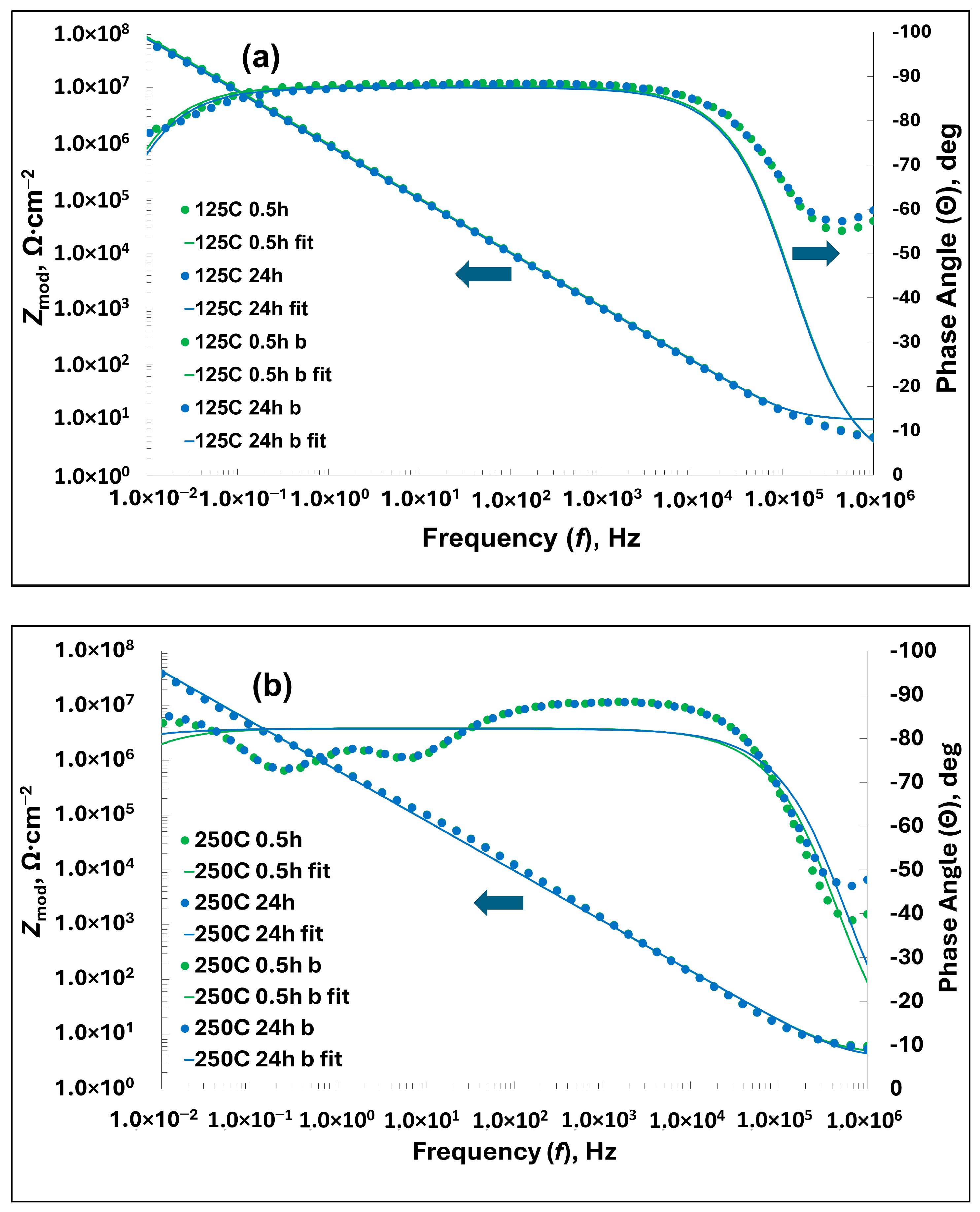
3.4. Electrochemical Studies

3.4.1. Results of the Voltammetry Measurements

The voltammetry measurement results of the coatings prepared at 125 and 250 °C presented in Figure 12 and Table 3 show that both nanolaminate coatings prepared by ALD notably reduce the corrosion current density, jcor, compared to the uncoated substrate. However, the lowest jcor value belongs to the sample coated at TG = 125 °C. Meanwhile, the current values at 2 V and pitting potential, Epit, values are better for the coating prepared at TG = 250 °C.

3.4.2. Results of the EIS Analyses

EIS measurements were carried out for the samples covered with the nanolaminates deposited at TG = 125, 200, 250, and 300 °C. Bode plots and electrical equivalent circuits (EC) used to fit the plots for the coatings prepared at TG = 125 and 250 °C after 0.5 and 24 h of immersion in 0.5 M NaCl solution are shown in Figure 13. The plots for the other two samples are shown in the Supplementary Materials in Figure S3.
An analysis of the Bode plots in Figure 13 and Figure S3 shows that the best corrosion protection is provided by the nanolaminate deposited at TG = 125 °C. For this coating, the Zmod value is the maximum at f = 10 mHz (74 MΩ) and decreases slightly after 24 h of immersion (67 MΩ), higher than for the other coatings prepared at higher temperatures. In addition, the logarithmic dependence of Zmod on the frequency is linear over a wide frequency band with a slope of −0.5, corresponding to the capacitor. This capacitive behavior extends to the low frequency end of the spectrum, 10 mHz, indicating that the charge transfer has very low kinetics. This is also consistent with the impedance phase angle plot, which is close to −90° over a wide frequency range. Ohmic resistance is measured only at high frequencies, such as f > 100 kHz. On the basis of the Bode plot in Figure 13a and the fitting parameters given in Table 4, it was found that a single time constant electrical equivalent circuit (EC), shown in Figure 13c, is sufficient to describe the SS substrate system coated with the nanolaminate prepared at 125 °C. This finding was somewhat surprising, because in our previous work, where a similar nanolaminate was deposited on an AISI 304 substrate, we found that the best choice is the EC with two time constants [43], which took into account defects, pores, and/or cracks in the laminate and the passivation coating of natural oxides on the surface of the SS substrate. After 24 h of immersion in the electrolyte solution, the Bode plot of the same graph shows little change compared to the first graph taken after a 0.5-h stabilization period, so it is difficult to distinguish between the two graphs. Only the initial value of Zmod is slightly reduced, as noted above, but the fitting parameters are practically the same. This indicates that the laminate practically does not change during 24 h of immersion and is well bound to the passivation layer, so that they formed a composite protective layer.
The Bode plots of the nanolaminate deposited at TG = 250 °C (Figure 13b) show almost the same behavior as the plots discussed above. Only the linearity of the Zmod~f plot is slightly disturbed, which may indicate some transient defects in the composite coating that disappeared during the self-healing process. Similarly, the impedance phase angle plot Θ~f is altered, especially in the low-frequency range, when compared with a similar plot in Figure 13a, which shows some changes in higher temperature coatings. Again, after 24 h of immersion, the Bode plots remained almost unchanged, with the exception of the resistance of the compound coating, Rlam, which was reduced by more than a factor of two. We tried to fit these Bode graphs using ECs with two time constants but were unsuccessful, because the errors of the fitting parameters reached values too large, exceeding the parameter values by several orders of magnitude for some parameters. We therefore decided to use the same EC with a single time constant to fit both Bode plots. On the basis of the fitting curves in Figure 13b and the fit parameters in Table 4, we can assess the quality of the fitting as satisfactory.
The Bode plots of the other analyzed samples show a deteriorating trend with the increasing TG (Figure S3). Thus, based on the EIS analyses, the laminates deposited at TG = 125 °C exhibited the best corrosion protection properties.

3.4.3. Immersion Tests

The results of the immersion test in 6% FeCl3 solution at 50 °C are shown in Figure 14 and Figure S4. Figure 14 shows SS samples with the nanolaminate coatings after a 72-h immersion test. Figure 14a shows that the fully amorphous coating prepared at 125 °C withstands the test well; pitting occurs mainly at the edges of the sample, probably due to the handling of the sample during the test. In contrast, the nanolaminate prepared at TG = 250 °C (Figure 14b) with crystalline titania sublayers is uniformly densely covered with corrosion pits.
A closer look at the images in Figure 14 reveals two types of defects on the surfaces of the objects. The light-colored dots represent shallower defects where the coating is damaged but corrosion does not penetrate deep into the metal. The dark spots are corrosion holes that penetrate deep into the metal. Only a few darker spots appear close to the edges of the samples with amorphous coating. On the 250 °C laminate, both light-colored and dark spots cover the whole surface area. Figure S4 shows the photographs of the samples prepared at 125, 200, 250, and 300 °C after 24, 48, and 72 h of immersion, with the marked areas within which the pits were counted. These images and Table 5 demonstrate the results of the immersion test on a time scale and show that coatings made at 125 °C passed and coatings made at ≥200 °C failed the test according to ASTM Standard Guide for Examination and Evaluation of Pitting Corrosion [3,44]. This guide classifies a coating as Class 1 if the number of pits is less than 2500 per square meter; thus, the 125 °C coating is classified as Class 1. At the same time, the laminate prepared at 160 °C is classified as Class 2, the coating at TG = 200 °C to Class 3, and the coatings with higher TG to Class 5.
Consequently, the immersion test results corroborate the EIS analysis result that a nanolaminate ceramic coating prepared with ALD at a low temperature (125 °C) is the most corrosion-resistant.

3.5. Mechanical Properties of the Laminated Coatings

Many practical applications of protective coatings require coatings with sufficient hardness and wear resistance, as well as good adhesion with the substrate materials. To characterize the mechanical properties and adhesion of the laminate deposited on the substrate, some samples were subjected to sonication and temperature shock in liquid nitrogen. We only tested samples deposited at TG = 250 and 300 °C, because the coatings deposited at TG ≤ 200 °C were mechanically weaker [45].
As evident in Figure 15a, even 10 min of sonication of the coating deposited on SS at 250 °C causes the laminate to fracture as particles of tens of micrometers are removed from the laminate. Similarly, the liquid N2 temperature shock removes and rolls large sublayer parts owing to the mechanical stresses between the sublayers of alumina and titania, as shown in Figure 15b. Meanwhile, the laminate deposited at 300 °C loses only small parts of the topmost sublayer(s) during three-times longer sonication (30 min), as imaged in Figure 15c, and similarly, the 300 °C sample immersed in liquid N2 for 20 s also exhibits small, detached coating particles, as shown in Figure 15d. Thus, an increase in TG leads to an increase in the hardness of the coating and its adhesion to the substrate.

4. Discussion

4.1. Role of the Metal Surface Pretreatment

In Section 3.4.2, we showed, based on the analysis of the Bode plots and their fitting parameters, that alumina/titania nanolaminate coatings, especially those prepared at 125 °C, appear to be of higher quality and display better adhesion to the passive natural oxide layer of the substrate than similar coatings studied in our previous work [30]. As the AISI 310 substrate contains more chromium, its natural oxide layer is likely to be composed of more chromium oxide and, therefore, have better passivation properties. However, another difference compared to this study is the pretreatment of the SS substrate. Notably, in another work [31], and also in the present study, we introduced the pretreatment of substrate etching in a hot solution of mixed mineral acids, which we described in the experimental part. In the study referred to above, this procedure helped to significantly improve the chemical resistance of the laminated coatings. The dependence of the coating quality on the pretreatment of the metal substrate surface is not surprising, since ALD is based on surface reactions, and the nucleation of the growing layers also depends on the surface properties. Thus, the work [27] also showed the dependence of the coating quality on the pretreatment of the metal substrate surface. Future studies could show which study modification has a greater impact on the quality of the protective coatings.

4.2. Porosity of the Coatings

ALD is known to cover surfaces with complex 3D topography with conformal thin films. Our HR-SEM and TEM analyses did not provide evidence of uncovered areas and cracks in the oxide layers/laminates grown with ALD. SEM/STEM images are shown in Figure 4b,c, Figure 5, Figure 8a,b, Figure 11a, and Figure S2a,b,d,e as examples. However, the pores or cracks could be generated into the coating during the open-circuit potential stabilization in the electrolyte before the electrochemical measurements or during the measurements. Therefore, porosity analysis is of particular importance. A number of electrochemical methods have been proposed to evaluate the porosity of the coating, an overview of which is given in [43,46,47]. We used a simple relationship for porosity analysis, which is presented in [43]. The porosity (P) can be estimated from the passivation current density obtained from the polarization curve taken at a potential of +0.2 V anodic to the OCP, which, for the coated sample, is denoted as jp and, for the bare sample, jp0:
P = j p j p 0 × 100 % .
Table 6 shows the values of the passive current density and estimated porosity. The amorphous laminate grown at 125 °C shows very low porosity, but the porosity of the laminate with crystalline titania sublayers deposited at 250 °C is much higher. Thus, the low-temperature laminate can be considered to form a good physical barrier that is in agreement with its electrochemical reaction in a chloride medium.

4.3. Potential Applicability of ALD Coatings in Industry

Actually, the ALD method has been applied in the microelectronics industry for many years [48]. It was possible with the development of pinhole-free oxide layers, e.g., isolating Al2O3, high-k ZrO2, and HfO2, or metal Cu and W layers. Also, the developments of atomic layer etching (ALE), in which surface layers are etched, and area selective ALD, in which some surface parts are without active sites, thus inhibiting the deposition process, allowed us to significantly reduce the number of process steps required for lithography following wet or dry etching. Another ALD development allowing us to carry the process out on relatively large planar surfaces fast is open air spatial ALD [49].
Regarding the use of ALD single films and laminates for the corrosion protection of metals, there are a number of conditions for the application of the method. Firstly, it is necessary to demonstrate the existence of an effective ALD corrosion protection coating technology and, secondly, to demonstrate the existence of, or at least the feasibility of constructing, industrially applicable ALD reactors capable of coating small and large objects. Thirdly, it is necessary to demonstrate the economic, as well as the increasingly important environmental, benefits of their use. The first point is the subject matter of the present study, but of course, different substrates may need the development of specific technologies. Regarding the second point, existing ALD reactors can be used to coat windowpanes, coins, small medical instruments, polymer and glass sunglasses, contact lenses, etc., all of which are already coated with ALD coatings. In the literature, there has been recent news about the development of a new small-size open air ALD setup, which could be introduced in industry, e.g., for coating welding seams [29]. Some authors of the present study were also connected with the introduction of ALD in corrosion protection at the industrial level; see patents [50,51]. The studies connected with these patents allowed us to project and introduce an industrial ALD setup for a worldwide company. Further developments are needed for introducing ALD into protection-specific industrial products, e.g., pipelines, water pipes and tanks, air- and spacecraft parts, etc. The third point is complex and crucial. The relevance of the present study to the third point was, in particular, the choice of the laminate materials, alumina and titanium. Here, among other properties, we took into account that one could use relatively cheap precursors (TMA, TiCl4, and H2O); that the resulting coatings would be light (Al2O3 and TiO2); and that the outer layer of the coatings would be TiO2, which is both environmentally safe and biofriendly.

5. Conclusions

Protective coatings with three-times (Al2O3/TiO2) nanometer-thick sublayers were grown with ALD for SS and Si substrates from inexpensive TMA and TiCl4 metal precursors and H2O as the oxygen precursor at a large TG range from 80 to 500 °C. The coatings were examined for resistance to chemical etching, corrosion, and physical treatments, such as sonication and rapid freezing with liquid N2. The main results and recommendations for the selection of an appropriate TG value for the ALD process are as follows:
  • All of the coatings tested provided a certain level of protection to both substrate types, but there is no ideal TG value that would guarantee the best performance for all the properties tested.
  • Coatings deposited at TG ≤ 100 °C had the lowest protective properties due to the high content of residual impurities resulting from incomplete surface reactions in the ALD processes.
  • The total growth rate of the coatings was higher and the chlorine residue content lower for the coatings deposited on SS substrates at TG = 100–125 °C compared to coatings deposited on Si substrates in the same run; the effect somewhat improves the performance of low-temperature ALD coatings in protecting SS substrates.
  • The best corrosion resistance appeared with a fully amorphous laminated coating deposited at 125 °C. Still, due to its poor abrasion resistance, it may need to be coated with a paint/varnish layer.
  • Coatings deposited at TG ≥ 250 °C showed the best resistance to chemical etching and the physical treatments due to the crystalline titania (anatase) sublayers. However, raising the TG to 500 °C will cause some decomposition of the aluminum precursor TMA.
  • The inhomogeneity of the interfaces in the laminates grown at 160 °C and initial crystallization of titania in the laminates grown at TG = 200 °C both increase the defectiveness of the coatings and lead to slowing the increase in the etching resistance efficiency and, at the same time, lead to a decrease in the corrosion protection of the coatings prepared at these temperatures. Thus, we do not recommend the use of this temperature range for the preparation of laminate coatings.

Supplementary Materials

The supporting information can be downloaded at: https://www.mdpi.com/article/10.3390/cmd6030036/s1.

Author Contributions

Conceptualization, V.S.; methodology, I.N., L.A., J.K., H.M., and V.S.; validation, I.N., L.A., and V.S.; formal analysis, I.N., L.A., and H.M.; investigation, I.N., L.A., J.K., A.T., M.M., K.A., P.R., and H.M.; resources, L.A., H.M., and V.S.; data curation, I.N. and V.S.; writing—original draft preparation, I.N.; writing—review and editing, V.S.; visualization, I.N.; supervision, V.S.; project administration, V.S.; funding acquisition, L.A. and V.S. All authors have read and agreed to the published version of the manuscript.

Funding

This research was funded by the Estonian Research Council through the projects IUT2-24, IUT20-54, TLTFY14054T, PSG448, PRG2594, and TEM-TA31 and by the Archimedes Foundation and the EU through the European Regional Development Fund under the project TK141 (2014-2020.4.01.15-0011).

Data Availability Statement

Data are available on request.

Acknowledgments

A. Kiisler is acknowledged for the help in sample preparation and H. Põldemaa for the help in some SEM measurements.

Conflicts of Interest

The authors declare no conflicts of interest.

Abbreviations

The following abbreviations are used in this manuscript:
AISIAmerican Iron and Steel Institute
SSStainless steel
ALDAtomic layer deposition
TMATrimethylaluminum
XRFX-ray fluorescence
EPMAElectron probe microanalysis
XRDX-ray diffraction
GIXRDGrazing incidence X-ray diffraction
PBParallel beam (geometry)
HR-SEMHigh-resolution scanning electron microscope
FIBFocused ion beam
SEMScanning electron microscope
STEMScanning transmission electron microscope
HR-(S)TEMHigh-resolution (scanning) transmission electron microscope
SCESaturated calomel electrode
LSVLinear sweep voltammetry
OCPOpen-circuit potential
EISElectrochemical impedance spectrometry
RMSRoot mean square
ACAlternating current
CPEConstant phase element
ASTMAmerican Society for Testing and Materials
GenAIGenerative artificial intelligence
BFBright field
HAADFHigh-angle annular dark field
RBSRutherford backscattered spectroscopy
TOF-ERDATime-of-flight elastic recoil detection analysis
EC(Electrical) equivalent circuit

Appendix A

Figure A1. Etching rates of the laminate sublayers depending on their growth temperature: (a) laminates on silicon substrates and (b) laminates on steel substrates.
Cmd 06 00036 g0a1

References

  1. McGuire, M. Stainless Steels for Design Engineers; ASM International: Novelty, OH, USA, 2008; pp. 161–171. [Google Scholar]
  2. Norton, J.; Baxter, D.; Santorelli, R.; Bregani, F. The corrosion of AISI 310 stainless steel exposed to sulphidizing/oxidizing/carburizing atmospheres at 600 °C. Corros. Sci. 1993, 35, 1085–1090. [Google Scholar] [CrossRef]
  3. Roberge, P.R. Handbook of Corrosion Engineering; McGraw-Hill: New York, NY, USA, 2000; ISBN 0-07-076516-2. [Google Scholar]
  4. Padhi, N.; Kamal, S.; Chandra, R.; Kamachi Mudali, U.; Raj, B. Corrosion performance of TiO2 coated type 304L stainless steel in nitric acid medium. Surf. Coat. Techol. 2010, 204, 2782–2788. [Google Scholar] [CrossRef]
  5. Sridharan, M.; Sillassen, M.; Bøttiger, J.; Chevallier, J.; Birkedal, H. Pulsed DC magnetron sputtered Al2O3 films and their hardness. Surf. Coatings Technol. 2007, 202, 920–924. [Google Scholar] [CrossRef]
  6. Bera, S.; Rout, T.K.; Udayabhanu, G.; Narayan, R. Comparative Study of Corrosion Protection of Sol–Gel Coatings with Different Organic Functionality on Al-2024 substrate. Progr. Org. Coat. 2015, 88, 293–303. [Google Scholar] [CrossRef]
  7. Lazar, A.-M.; Yespica, W.P.; Marcelin, S.; Pébère, N.; Samélor, D.; Tendero, C.; Vahlas, C. Corrosion protection of 304L stainless steel by chemical vapor deposited alumina coatings. Corros. Sci. 2014, 81, 125–131. [Google Scholar] [CrossRef]
  8. Sugama, T. CVD-titanium carbonitride coatings as corrosion-preventing barriers for steel in acid-brine steam at 200 °C. Mater. Lett. 1999, 38, 227–234. [Google Scholar] [CrossRef]
  9. Lauwerens, W.; De Boeck, A.; Thijs, M.; Claessens, S.; Van Stappen, M.; Steenackers, P. PVD Al–Ti and Al–Mn coatings for high temperature corrosion protection of sheet steel. Surf. Coat. Technol. 2001, 146, 27–32. [Google Scholar] [CrossRef]
  10. Leskelä, M.; Ritala, M. Review Atomic layer deposition (ALD): From precursors to thin film structures. Thin Solid Films 2002, 409, 138–146. [Google Scholar] [CrossRef]
  11. Matero, R.; Ritala, M.; Leskelä, M.; Salo, T.; Aromaa, J.; Forsen, O. Atomic layer deposited thin films for corrosion protection. J. Phys. IV 1999, 9, 493–499. [Google Scholar] [CrossRef]
  12. Shan, C.X.; Hou, X.; Choy, K.-L. Corrosion Resistance of TiO2 Films Grown on Stainless Steel by Atomic Layer Deposition. Surf. Coatings Technol. 2008, 202, 2399–2402. [Google Scholar] [CrossRef]
  13. Abdulagatov, A.I.; Yan, Y.; Cooper, J.R.; Zhang, Y.; Gibbs, Z.M.; Cavanagh, A.S.; Yang, R.G.; Lee, Y.C.; George, S.M. Al2O3 and TiO2 Atomic layer deposition on copper for water corrosion resistance. Appl. Mater. Interfaces 2011, 3, 4593–4601. [Google Scholar] [CrossRef]
  14. Correa, G.C.; Bao, B.; Strandwitz, N.C. Chemical Stability of Titania and Alumina Thin Films Formed by Atomic Layer Deposition. ACS Appl. Mater. Interfaces 2015, 7, 14816–14821. [Google Scholar] [CrossRef]
  15. Marin, E.; Lanzutti, A.; Guzman, L.; Fedrizzi, L. Chemical and electrochemical characterization of TiO2/Al2O3 atomic layer depositions on AZ-31 magnesium alloy. J. Coat. Technol. Res. 2012, 9, 347–355. [Google Scholar] [CrossRef]
  16. Merisalu, M.; Aarik, L.; Piirsoo, H.-M.; Kozlova, J.; Tarre, A.; Zabels, R.; Wessing, J.; Brieva, A.; Sammelselg, V. Nanostructured Coating for Aluminum Alloys Used in Aerospace Applications. J. Electrochem. Soc. 2022, 169, 071503. [Google Scholar] [CrossRef]
  17. Marin, E.; Lanzutti, A.; Guzman, L.; Fedrizzi, L. Corrosion protection of AISI 316 stainless steel by ALD alumina/titania nanometric coatings. J. Coatings Technol. Res. 2011, 8, 655–659. [Google Scholar] [CrossRef]
  18. Marin, E.; Guzman, L.; Lanzutti, A.; Ensinger, W.; Fedrizzi, L. Multilayer Al2O3/TiO2 Atomic Layer Deposition coatings for the corrosion protection of stainless steel. Thin Solid Film. 2012, 522, 283–288. [Google Scholar] [CrossRef]
  19. Härkönen, E.; Diaz, B.; Swiatowska, J.; Maurice, V.; Seyeux, A.; Vehkamäki, M.; Sajavaara, T.; Fenker, M.; Marcus, P.; Ritala, M. Corrosion protection of steel with oxide nanolaminates grown by Atomic Layer Deposition. J. Electrochem. Soc. 2011, 158, C369–C378. [Google Scholar] [CrossRef]
  20. ISO9227:2022; Corrosion Tests in Artificial Atmospheres—Salt Spray Tests. The International Organization for Standardization (ISO): Geneva, Switzerland, 2022. Available online: https://www.iso.org/standard/81744.html (accessed on 27 July 2025).
  21. Kong, J.-Z.; Xu, P.; Cao, Y.-Q.; Li, A.-D.; Wang, Q.-Z.; Zhou, F. Improved corrosion protection of CrN hard coating on steel sealed with TiOxNy-TiN composite layers. Surf. Coat. Technol. 2020, 381, 125108. [Google Scholar] [CrossRef]
  22. Lim, J.W.; Yun, S.J.; Kim, H.-T. Characteristics of AlxTi1−xOy films grown by Plasma-Enhanced Atomic Layer. J. Electrochem. Soc. 2007, 154, G239–G243. [Google Scholar] [CrossRef]
  23. Kukli, K.; Ritala, M.; Leskelä, M.; Sundqvist, J.; Oberbeck, L.; Heitmann, J.; Schröder, U.; Aarik, J.; Aidla, A. Influence of TiO2 incorporation in HfO2 and Al2O3 based capacitor dielectrics. Thin Solid Film. 2007, 515, 6447–6451. [Google Scholar] [CrossRef]
  24. Jõgi, I.; Kukli, K.; Kemell, M.; Ritala, M.; Leskelä, M. Electrical characterization of AlxTiyOzmixtures and Al2O3–TiO2–Al2O3 nanolaminates. J. Appl. Phys. 2007, 102, 114114. [Google Scholar] [CrossRef]
  25. Abaffy, N.B.; McCulloch, D.G.; Partridge, J.G.; Evans, P.J.; Triani, G. Engineering titanium and aluminum oxide composites using atomic layer deposition. J. Appl. Phys. 2011, 110, 123514. [Google Scholar] [CrossRef]
  26. Härkönen, E.; Diaz, B.; Swiatowska, J.; Maurice, V.; Seyeux, A.; Fenker, M.; Toth, L.; Radnoczi, G.; Marcus, P.; Ritala, M. AlxTayOz Mixture coatings prepared using Atomic Layer Deposition for corrosion protection of steel. Chem. Vap. Depos. 2013, 19, 194–203. [Google Scholar] [CrossRef]
  27. Daubert, J.S.; Hill, G.T.; Gotsch, H.N.; Gremaud, A.P.; Ovental, J.S.; Philip, S.; Williams, P.S.; Oldham, C.N.; Gregory, N.; Parsons, G.N. Corrosion Protection of Copper Using Al2O3, TiO2, ZnO, HfO2, and ZrO2 Atomic Layer Deposition. ACS Appl. Mater. Interfaces 2017, 9, 4192–4201. [Google Scholar] [CrossRef] [PubMed]
  28. Li, J.; Yan, C.; Dai, Y.; Lan, Z.; Liu, C. Electrochemical and structural properties of ultrathin atomic layer deposition coatings for corrosion resistance on aluminum alloy. Ceram. Int. 2025, 51, 12123–12137. [Google Scholar] [CrossRef]
  29. Santinacci, L. Atomic layer deposition: An efficient tool for corrosion protection. Curr. Opin. Colloid Interface Sci. 2023, 63, 101674. [Google Scholar] [CrossRef]
  30. Sammelselg, V.; Netšipailo, I.; Aidla, A.; Tarre, A.; Aarik, L.; Asari, J.; Ritslaid, P.; Aarik, J. Chemical resistance of thin film materials based on metal oxides grown by atomic layer deposition. Thin Solid Films 2013, 542, 219–224. [Google Scholar] [CrossRef]
  31. Aarik, L.; Kozlova, J.; Mändar, H.; Aarik, J.; Sammelselg, V. Chemical resistance of TiO2 and Al2O3 single-layer and multilayer coatings atomic layer deposited from hydrogen-free precursors on silicon and stainless steel. Mater. Chem. Phys. 2019, 228, 285–292. [Google Scholar] [CrossRef]
  32. Arroval, T.; Aarik, L.; Rammula, R.; Kruusla, V.; Aarik, J. Effect of substrate-enhanced and inhibited growth on atomic layer deposition and properties of aluminum-titanium oxide films. Thin Solid Films 2016, 600, 119–125. [Google Scholar] [CrossRef]
  33. Pärna, R.; Nõmmiste, E.; Kikas, A.; Jussila, O.; Hirsimäki, M.; Valden, M.; Kisand, V. Electron spectroscopic study of passive oxide layer formation on Fe-19Cr-18Ni-1Al-TiC austenitic stainless steel. J. Electron Spectrosc. Relat. Phenom. 2010, 182, 108–114. [Google Scholar] [CrossRef]
  34. Sammelselg, V.; Rauhala, E.; Arstila, K.; Zakharov, A.; Aarik, J.; Kikas, A.; Karlis, J.; Tarre, A.; Seppälä, A.; Asari, J.; et al. Study of thin oxide films by electron, ion, and synchrotron radiation beams. Microchim. Acta 2002, 139, 165–169. [Google Scholar] [CrossRef]
  35. Brug, G.J.; Van den Eeden, A.L.G.; Sluyters-Rehbach, M.; Sluyters, J.H. The analysis of electrode impedances complicated by the presence of a constant phase element. J. Electroanal. Chem. Interfacial Electrochem. 1984, 176, 275–295. [Google Scholar] [CrossRef]
  36. Zoltowski, P. On the electrical capacitance of interfaces exhibiting constant phase element behavior. J. Electroanal. Chem. 1998, 443, 149–154. [Google Scholar] [CrossRef]
  37. ASTM G48-11(2020)e1; Standard Test Methods for Pitting and Crevice Corrosion Resistance of Stainless Steels and Related Alloys by Use of Ferric Chloride Solution. ASTM International: West Conshohocken, PA, USA, 2020.
  38. Mamedov, S. Characterization of TiO2 Nanopowders by Raman Spectroscopy. Spectrosc. Suppl. 2020, 35, 41–49. [Google Scholar]
  39. Aarik, J.; Aidla, A.; Kiisler, A.; Uustare, T.; Sammelselg, V. Effect of crystal structure on optical properties of TiO2 films grown by atomic layer deposition. Thin Solid Films 1997, 305, 270–273. [Google Scholar] [CrossRef]
  40. Sammelselg, V.; Tarre, A.; Lu, J.; Aarik, J.; Niilisk, A.; Uustare, T.; Netšipailo, I.; Rammula, R.; Pärna, R.; Rosental, A. Structural characterization of TiO2–Cr2O3 nanolaminates grown by atomic layer deposition. Surf. Coatings Technol. 2010, 204, 2015–2018. [Google Scholar] [CrossRef]
  41. Aarik, J.; Aidla, A.; Mändar, H.; Sammelselg, V. Anomalous effect of temperature on atomic layer deposition of titanium dioxide. J. Cryst. Growth 2000, 220, 531–537. [Google Scholar] [CrossRef]
  42. Iatsunskyi, I.; Coy, E.; Viter, R.; Nowaczyk, G.; Jancelewicz, M.; Baleviciute, I.; Załęski, K.; Jurga, S. Study on Structural, Mechanical, and Optical Properties of Al2O3−TiO2 Nanolaminates Prepared by Atomic Layer Deposition. J. Phys. Chem. C 2015, 119, 20591–20599. [Google Scholar] [CrossRef]
  43. Mondal, J.; Marques, A.; Aarik, L.; Kozlova, J.; Simões, A.; Sammelselg, V. Development of a Thin Ceramic-Graphene Nanolaminate Coating for Corrosion Protection of Stainless Steel. Corros. Sci. 2016, 105, 161–169. [Google Scholar] [CrossRef]
  44. ASTM G46–94; Standard Guide for Examination and Evaluation of Pitting Corrosion. American Society for Testing of Materials: West Conshohocken, PA, USA, 1999.
  45. Ylivaara, O.M.E.; Langner, A.; Liu, X.; Schneider, D.; Julin, J.; Arstila, K.; Sintonen, S.; Ali, S.; Lipsanen, H.; Sajavaara, T.; et al. Mechanical and optical properties of as-grown and thermally annealed titanium dioxide from titanium tetrachloride and water by atomic layer deposition. Thin Solid Films 2021, 732, 138758. [Google Scholar] [CrossRef]
  46. Tato, W.; Landolt, D. Electrochemical determination of the porosity of single and duplex PVD coatings of titanium and titanium nitride on brass. J. Electrochem. Soc. 1998, 145, 4173–4181. [Google Scholar] [CrossRef]
  47. Díaz, B.; Światowska, J.; Maurice, V.; Seyeux, A.; Normand, B.; Härkönen, E.; Ritala, M.; Marcus, P. Electrochemical and time-of-flight secondary ion mass spectrometry analysis of ultra-thin metal oxide (Al2O3 and Ta2O5) coatings deposited by atomic layer deposition on stainless steel. Electrochim. Acta 2011, 56, 10516–10523. [Google Scholar] [CrossRef]
  48. Chou, N.H. Atomic Layer Deposition: Significance and Application in Modern Microelectronics. Available online: https://www.materion.com/en/insights/blog/atomic-layer-deposition-significance-application-in-modern-microelectronics (accessed on 13 July 2025).
  49. Sekkat, A.; Weber, M.; López-Sánchez, J.; Rabat, H.; Hong, D.; Rubio-Zuazo, J.; Bellet, D.; Chichignoud, G.; Kaminski-Cachopo, A.; Muñoz-Rojas, D. Selective spatial atomic layer deposition of Cu, Cu2O and CuO thin films in the open air: Reality or fiction? Mater. Today Chem. 2023, 29, 101431. [Google Scholar] [CrossRef]
  50. Sammelselg, V.; Aarik, L.; Merisalu, M. Method of Preparing Corrosion Resistant Coatings. WO2014102758A1, 3 July 2014. Available online: http://www.google.com/patents/WO2014102758A1?cl=en (accessed on 27 July 2025).
  51. Sammelselg, V.; Kostamo, J.; Bayerl, W.; Aarik, J.; Aarik, L.; Lindfors, S.; Adam, P.; Poutianen, J. Protecting an Interior of a Gas Container with an ALD Coating. WO20151324443A1, 11 September 2015. Available online: http://www.google.com/patents/WO2015132443A1?cl=en (accessed on 27 July 2025).
Figure 1. Graph of the changes of the sublayer thicknesses during the etching process, as determined after each etching step.
Cmd 06 00036 g001
Figure 2. Raman spectra of the laminates grown at different temperatures on (a) Si (100) and (b) SS substrates. Letter A indicates the bands connected with the anatase phase of titania, and the numbers in brackets show the band peak position in cm−1.
Cmd 06 00036 g002
Figure 3. GIXRD patterns of the laminates grown at different temperatures on different substrates: (a) Si (100) and (b) AISI 310 stainless steel. The letter A denotes the peaks associated with the anatase phase of the titania sublayers, and the numbers following it denote the hkl values of the corresponding atomic planes of diffraction.
Cmd 06 00036 g003
Figure 4. Surface images of bare SS (a) and SS with laminated coatings deposited at 160 °C (b) and 300 °C (c). SEM secondary electron images.
Cmd 06 00036 g004
Figure 5. Cross-section images of the 3× (Al2O3/TiO2) nanolaminates grown at (a) 160 and (b) 300 °C on Si substrates and (c) at 250 °C on a steel substrate. HR-SEM images in bright field (BF) STEM mode.
Cmd 06 00036 g005
Figure 6. Etching resistance efficiency, Re, dependence on the growth temperature, TG, of the protective laminate coatings deposited on (a) the Si and (b) SS substrates.
Cmd 06 00036 g006
Figure 7. SEM images of etched nanolaminate coatings grown on AISI 310 stainless steel at (a) TG = 100 °C etched within 2 min, during which ~10% of the coating thickness is lost, and at (b) TG = 125 °C etched within 5 min; in image (a), the blisters are marked with white arrows and cracks with yellow arrows.
Cmd 06 00036 g007
Figure 8. SEM images of (a,b) non-etched and (c,d) etched (for 5 min) laminate grown at 250 °C onto the SS substrate; (a,c) surface view at different magnifications, and the (b,d) cross-section view demonstrating the outer sublayers partly etched away and marked with arrows (c,d); the topographical contrast is enhanced via (a,c) a secondary electron signal using a 10-keV probe and composition contrast via (b,d) a backscattered electron signal and 20-keV probe.
Cmd 06 00036 g008aCmd 06 00036 g008b
Figure 9. Cross-section lamella of an etched laminated coating deposited onto the SS substrate at 400 °C; upper part is the SS substrate. SEM image in STEM mode.
Cmd 06 00036 g009
Figure 10. Cross-section of the coated Si samples exhibiting the laminate deposited at (a) 160 °C (arrow shows a nanocrystallite or defect; HR-SEM BF STEM image) and (b) 200 °C (HR-STEM BF images); the Si substrate is above in image (a) and below in image (b); the insets are HR-TEM BF images with higher magnifications.
Cmd 06 00036 g010
Figure 11. HR-STEM images of the cross-section of the laminate deposited onto the SS substrate at 200 °C: (a) overview (BF image) and (b) crystalline part of a titania sublayer (HAADF image).
Cmd 06 00036 g011
Figure 12. Voltammetry measurement results. (a) LSV and (b) cyclic voltammetry curves for the uncoated (curve 1) and ALD-coated laminates prepared at 125 and 250 °C (curves 2 and 3, respectively).
Cmd 06 00036 g012
Figure 13. Bode plots after 0.5 and 24 h of immersion in 0.5 M NaCl solution for the coatings prepared at (a) 125 and (b) 250 °C.
Cmd 06 00036 g013
Figure 14. Digital photos of the samples coated with the nanolaminate after the 72-h immersion test in FeCl3 solution: nanolaminates grown at (a) 125 and (b) 250 °C. The displayed area of the samples is 4 × 4 cm2.
Cmd 06 00036 g014
Figure 15. SEM images of the surface of the laminate grown at 250 °C on the SS substrate (a) after 10 min of sonication and (b) after embedding into liquid nitrogen for 20 s, and of the laminate grown at 300 °C on the SS (c) after 30 min of sonication and (d) after embedding into liquid nitrogen for 20 s.
Cmd 06 00036 g015
Table 1. Data on the coatings and their etchings.
TG, °CCrystal Structure of Titania SublayersCoatings on Si SubstratesCoatings on AISI310 Substrates
Initial Thickness 1, d0, nmEtching Rate 2, ke, nm/sEtching Time, minInitial Thickness, nmEtching Rate 2, ke, nm/sEtching Time, min
TiO2Al2O3TiO2Al2O3
80Amorphous106.00.370.701108.20.090.095
Amorphous110.0 0.780.821157.10.180.164
100Amorphous107.00.100.153130.40.080.075
Amorphous111.3 0.170.163138.10.080.075
125Amorphous133.00.030.0510111.90.050.0410
Amorphous138.0 0.050.047.5121.30.040.057.5
160Amorphous?92.40.060.157.5117.90.030.015
Amorphous?118.0 0.060.067.5115.90.040.045
200Amorphous with nanocrystallites143.90.080.247.5133.00.110.093
Amorphous with nanocrystallites148.80.070.277.5207.40.140.073
250Crystalline (anatase)115.70.000.0110109.50.010.0110
Crystalline (anatase)102.20.020.0430110.40.010.0210
300Crystalline (anatase)93.40.000.0010126.30.000.0010
Crystalline (anatase)94.60.010.026096.40.020.0310
400Crystalline (anatase)94.00.000.001086.10.010.0210
Crystalline (anatase)82.90.010.033093.70.020.027.5
Crystalline (anatase)82.90.010.0260----
500Crystalline (anatase)88.60.010.0210171.80.000.027.5
Crystalline (anatase)104.10.000.043092.00.000.025
1 Uncertainty of d0 is ±10%. 2 Uncertainty of ke is ±20%.
Table 2. Compositions of the laminates deposited at different TG onto different substrates.
TG/substrateCoating Mass thickness, µg/cm2Element Content,
mass%
COAlTiClRatio for Cl 1
100 °C/Si 231.601.2 ± 0.941.0 ± 1.124.6 ± 0.130.4 ± 1.02.8 ± 0.21.2
100 °C/SS45.812.5 ± 0.142.1 ± 0.321.9 ± 0.0131.1 ± 0.12.4 ± 0.1
125 °C/Si23.183.1 ± 0.236.9 ± 0.225.5 ± 0.0232.5 ± 0.12.0 ± 0.21.4
125 °C/SS35.215.3 ± 0.136.7 ± 0.327.1 ± 0.0129.5 ± 0.11.4 ± 0.2
1 Ratio of the chlorine content of the coatings on the Si and SS substrates. 2 The slightly higher uncertainty of the measured concentration is due to the use of a smaller diaphragm (∅ = 1 mm) for the measurement of this smaller sample compared to the larger diaphragm (∅ = 10 mm) used for the other analyses.
Table 3. Voltammetry results of uncoated and coated SS substrates at different temperatures.
SamplesParameters 1
jcor, nAj−0.1 V, nAjmax; 2 V, mAEpit, V
Bare SS49.02441051.1
Coated SS: 125 °C0.040.57.21.3
Coated SS: 250 °C0.821.90.06>2.0
1 Uncertainty of j and E is ±10%.
Table 4. Bode experimental data and plot fitting parameters.
Samples (TG, Immersion Time)Experimental Data 1Parameters 2,3
Zmod(10 mHz),
Ω cm−2
Θmax,
deg
Rs,
Ω cm−2
Rlam,
Ω cm−2
nQlam,
F cm−2 sn−1
χ2
125 °C, 0.5 h7.4 × 107−88.53.53.7 × 1080.971.8 × 1070.017
125 °C, 24 h6.7× 107−88.33.23.2 × 1080.961.9× 1070.018
250 °C, 0.5 h3.9× 107−88.44.34.7 × 1080.922.9× 1070.035
250 °C, 24 h3.8× 107−88.33.42.1 × 1080.912.9× 1070.034
1 The experimental data are as follows: Zmod—impedance module and Θmax—impedance phase angle. 2 The fitting parameters are as follows: Rs—resistance of the electrolyte solution, Rlam—resistance of the laminate, n, and Qlam—the exponent and capacitance parameter of constant phase element, respectively (see Formula (4)), and χ2—statistical parameter evaluating the goodness of the fitting. 3 On the basis of the quality of the data fits, uncertainties are estimated to be ±15% of the value given for the 125 °C coatings and ±20% for the 250 °C coatings.
Table 5. Results of the standard ASTM G48A immersion test.
Sample TG,
°C
Number of Pits During ImmersionFinal Pit Density, m−2
24 h48 h72 h
Bright PitsDark PitsAll PitsBright PitsDark PitsAll PitsBright PitsDark PitsAll Pits
125-112-23-31.9 × 10³
2003161931477870481187.4 × 104
25012223227193781532311.4 × 105
300102131384078971152121.3 × 105
Table 6. Porosity of the ALD nanolaminated coatings.
Sample/Parameterjp0,
A·cm−2
jp,
A·cm−2
P,
%
SS/Laminate (125 °C)4.92 × 10−84.76 × 10−110.097
SS/Laminate (250 °C)9.44 × 10−101.92
Disclaimer/Publisher’s Note: The statements, opinions and data contained in all publications are solely those of the individual author(s) and contributor(s) and not of MDPI and/or the editor(s). MDPI and/or the editor(s) disclaim responsibility for any injury to people or property resulting from any ideas, methods, instructions or products referred to in the content.

