Abstract
The electromagnetic density of states (EM-DOS) plays a crucial role in understanding light–matter interactions, especially at metal–dielectric interfaces. This study explores the impact of interface geometry, material properties, and nanostructures on EM-DOS, with a focus on surface plasmon polaritons (SPPs) and evanescent waves. Using a combination of analytical and numerical methods, the behavior of EM-DOS is analyzed as a function of distance from metal–dielectric interfaces, showing exponential decay with penetration depth. The influence of different metals, including copper, gold, and silver, on EM-DOS is examined. Additionally, the effects of dielectric materials, such as Ti, PMMA, and , on the enhancement of electromagnetic field confinement are discussed. The study also investigates the effect of nanostructures, like nanohole and nanopillar arrays, on EM-DOS by calculating effective permittivity and analyzing the interaction of quantum emitters with these structures. Results show that nanopillar arrays enhance EM-DOS more effectively than nanohole arrays, especially in the visible spectrum. The findings provide insights into optimizing plasmonic devices for applications in sensing, quantum technologies, and energy conversion.
1. Introduction
The nanophotonics community has always sought to manipulate light at the nanoscale [1]. Therefore, understanding the interaction between nanostructures and quantum emitters in the near field is essential for advancing technologies in this field of knowledge [2]. The electromagnetic density of states (EM-DOS) is a versatile tool with applications in nanooptics and emerging technologies, particularly at dimensions far below the wavelength of light [3]. EM-DOS is a physical concept applied to the study of light–matter interactions at the nanoscale, which allows for engineering and controlling the behavior of photons in materials or structures, depending on the optical properties and geometry of the system or environment [4,5]. In the context of electromagnetic waves, the EM-DOS concept describes the density of available electromagnetic modes at a specific point in space for a given wavelength [6]. Two categories exist for electromagnetic modes: propagating modes and evanescent modes [7]. Propagating modes travel through a medium or space, typically characterized by a propagation vector, over distances without significant decay. In contrast, waves that decay exponentially with distance from the source characterize evanescent modes with an imaginary wavevector describing the behavior of electromagnetic fields near the material boundaries.
In plasmonics, electromagnetic waves are manipulated and controlled at the nanoscale, leading to various applications and phenomena [8,9,10,11]. A single metallic gold–dielectric interface is an example of a source of electromagnetic waves that can support surface plasmon resonances (SPRs) [12,13]. These SPRs lead to enhanced field confinement near the interface [14]. Exploiting this local electromagnetic field enhancement facilitates increased interactions between light and matter for applications. Coupling between evanescent waves and propagating surface plasmon polaritons (SPPs) at the interface of a semi-infinite metal and a dielectric significantly modifies the EM-DOS, altering the local spatial distribution of electromagnetic fields near the interface [12]. These coupled modes are strongly dependent on the dielectric function of materials, the geometry of the interface, and the properties of the incident light [15]. As a result, the interaction of the electromagnetic field and the local environment can enhance or suppress the spontaneous emission rates and fluorescence characteristics of nearby quantum emitters [16]. A significant aspect in the coupling and modulation of fluorescence near plasmonic structures is the modification of the spontaneous emission rate of a quantum emitter (QE) through its interaction with a resonant optical cavity, resulting in Purcell-enhanced fluorescence [16,17,18,19]. Therefore, the EM-DOS is modified locally when the QE is near the metallic–dielectric interface [20]. Thus, the density of states plays an important role in light–matter interactions, including spontaneous emission (fluorescence), thermal emission, and absorption. The fluorescence spectrum of a QE, such as a color center nitrogen vacancy (NV) or another nanoscale system, provides information about the intensity of the emitted light at different wavelengths [16]. Plasmonic nanostructures, such as nanoantennas, can enhance the fluorescence of nearby QE by increasing the local electromagnetic field intensity near the metal surface [20], leading to higher excitation and emission rates [21,22]. An example is the fluorescence from color centers, such as nitrogen-vacancy centers in diamond, where photon emission is associated with electronic transitions involving the NV spin states [23,24]. The coupling between the electromagnetic field of the QE and the metallic or dielectric surface depends on the emission frequency of the QE [16], and it is influenced by several factors, including the Purcell factor [25], the field enhancement factor [26], and both radiative and non-radiative decay rates [27].
SPR sensors are widely used to detect changes in the local environment near a metal surface by monitoring shifts in the resonance angle or wavelength [28,29]. The study of EM-DOS in these systems not only supports advancements in quantum optics and single-photon source development [30], but also extends to modern terahertz (THz) technologies. For instance, control over EM-DOS can be advantageous for optimizing plasmonic photoconductive THz antennas [31,32] and enabling high-order THz harmonic generation in two-dimensional materials with engineered lattice structures [33]. This diversity of applications highlights the fundamental role of EM-DOS in governing light–matter interactions at the sub-wavelength scale [34,35], making its study essential for the continued advancement of both classical and quantum technologies.
2. Theoretical Framework
As the introduction highlights, the EM-DOS is a parameter that characterizes the density of electromagnetic modes accessible for light–matter interactions in nanoscale structures, being highly sensitive to changes at the nanoscale, providing information about the density of electromagnetic states in confined volumes, and making it an invaluable tool for characterizing and manipulating optical properties at sub-wavelength dimensions. Some of the primary contributions to EM-DOS in free space come from the electromagnetic field of the punctual source (QE) as Figure 1 illustrates, and thermal emission near an interface arises due to resonant surface waves, to mention a few. Equation (1) expresses EM-DOS in terms of the squared electric field amplitude of the electromagnetic modes in a free-space environment [35]:
where is the EM-DOS in free space, is the angular frequency, and c the speed of light in free space. However, two contributions of electromagnetic modes, propagating and evanescent modes, describe the EM-DOS. Both propagating and evanescent modes play a fundamental role in shaping the EM-DOS and determining how light–matter interactions occur in nanoscale structures and interfaces. EM-DOS is essential in studying light–matter interactions at the nanoscale, contributing to advancements in nanophotonics applications such as enhanced emission and absorption, nanoantennas and metasurfaces, and single-photon sources. However, in the simplest case, a metallic–dielectric interface (Figure 1b) can modify the boundary conditions near a QE, which can affect the EM-DOS components and the behavior of the electromagnetic field emission of QE. When light interacts with an interface, the electromagnetic environment influences the EM-DOS, which, in turn, affects the reflection and transmission of light at interfaces.
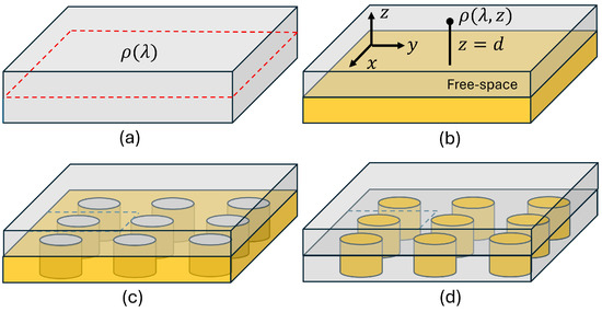
Figure 1.
Plasmonic structures analyzed in this study: (a) free space (reference), (b) semi-infinite metallic medium, (c) metallic nanohole array, and (d) metallic nanopillar array.
As illustrated in Figure 1b, the presence of an interface modifies the interaction characteristics between the incident wave and the interface. Furthermore, reflection, transmission, and absorption are intrinsic characteristics of electromagnetic waves interacting with material interfaces [36]. The Fresnel coefficients determine the amount of light reflected, transmitted, or absorbed at an interface between materials with different dielectric constants, such as free space and a dielectric or a metal. Factors like the angle of incidence and the materials’ properties influence the reflection coefficient R. In turn, the reflected light can interact, modifying the DOS of nearby structures or materials. The Fresnel coefficients determine the intensity and spatial distribution of electromagnetic fields at the interface, describing how reflection and transmission modify the electromagnetic fields. For the case of reflectivity, the equations for s and p polarizations for a single interface are given by the following expressions [37]:
where denotes the dielectric permittivity of the incident (superstrate) medium, and corresponds to the dielectric permittivity of the substrate (plasmonic) medium.
Fresnel coefficients play a significant role in determining the electromagnetic field distribution near interfaces, surfaces, and within layered structures, and the interaction of light with these structures influences the EM-DOS in the localized regions where these interactions occur. Some of the optical parameters of a metallic–dielectric interface that can significantly influence EM-DOS and the behavior of a QE are the dielectric constant (), the thickness of the material’s layer, and the materials (i.e., gold and silver) [38]. In a system at equilibrium temperature T, in the case of an open, absorbing medium like metal characterized by a complex frequency-dependent dielectric function , can express the spectral function, which is intricately linked to the imaginary component of Green’s function. The relationship is often given by [39]
where and are the dyadic Green functions of the electric and magnetic fields, respectively. In this case, the EM-DOS comprises electric and magnetic contributions as . The framework for EM-DOS at a given frequency at a given height z above the interface in free space has been calculated previously for a trapped atom near an interface at room temperature [40]. However, Joulian et al. [35] clearly define the EM-DOS in terms of Fresnel reflection factors and . In our study, we have expressed this definition as a function of wavelength rather than angular frequency, as this approach offers practical advantages and aligns more closely with experimental practices and material properties commonly used in optics and photonics. is calculated for a metallic interface in terms of the Fresnel reflection coefficients on the surface at the distance z to the surface by the following formula:
where and are defined as
where k denotes the normalized in-plane wavevector component, defined as , where is the in-plane wavevector and is the free-space wavenumber. Additionally,
with z being the perpendicular distance from the metallic plane surface. The range corresponds to propagating waves, whereas corresponds to evanescent waves’ contribution to EM-DOS. In Fresnel equations, the expression is used to describe evanescent waves during total internal reflection. When the incident angle exceeds the critical angle, Snell’s law () shows that the transmitted angle, , becomes complex, and no real wave propagates into the second medium. Instead, an evanescent wave forms, exponentially decaying along the interface. The sine of the angle of incidence relates to the normalized wavevector as . When is complex, becomes , where corresponds to the evanescent wave. At a fixed distance from the metal–dielectric interface, the EM-DOS depends on and . Making the Fresnel reflection factors zero allows retrieval of the free-space environment, which occurs when . Green’s function describes the behavior of electromagnetic fields in any material medium. By utilizing this information with the Green function, we can find the electromagnetic modes of the density of states associated with the system environment. The EM-DOS can influence the spontaneous emission rate of a QE, represented by , of an emitter placed in that environment, affecting the decay time. The inverse of is called the decay time (). The spontaneous emission rate at position is given by [38]
with being the wavelength, the dipole moment of the light emitter, the EM-DOS at position , and ℏ the reduced Planck constant. The density of electromagnetic modes accessible for emission influences the emitter’s spontaneous emission rate, which depends on its inherent characteristics and surroundings. The EM-DOS governs the efficiency of plasmonic systems. A plasmonic system refers to a class of nanostructured materials or devices that exploit surface plasmon resonances to manipulate and control light at the nanoscale. When light interacts with these nanostructures, it can couple with the surface plasmons, leading to phenomena like enhanced electromagnetic fields, light confinement, and resonant absorption or scattering of light. Positioning an emitter close to a metallic nanostructure that supports surface plasmon modes alters the local density of optical states because of the high field confinement characteristic of surface plasmons. This modification can lead to an increase in the spontaneous emission rate of the emitter [41], a phenomenon known as “spontaneous emission enhancement”.
3. Results and Discussion
EM-DOS determines the density of available electromagnetic modes at a specific location, . Locations near interfaces can be significantly enhanced due to surface plasmon resonances and evanescent waves being important for designing devices like sensors, photodetectors, and solar cells that maximize light–matter interactions. Additionally, the geometry and material properties of an interface affect the EM-DOS. Optical resonances that enhance specific wavelengths can be created by tuning the interface. For example, we can design plasmonic nanostructures to resonate in the UV, VIS, or IR regions, enabling applications like surface-enhanced spectroscopy. In quantum optics, QEs, such as color center NV, also benefit from enhanced EM-DOS. This enhancement increases the spontaneous emission rate, making these emitters brighter. For single-photon sources, maximizing EM-DOS is essential for efficient photon emission, and different materials exhibit varying EM-DOS behavior. Figure 2 shows EM-DOS in a free space and a metallic (Au) semi-infinite surface across VIS and IR wavelengths.
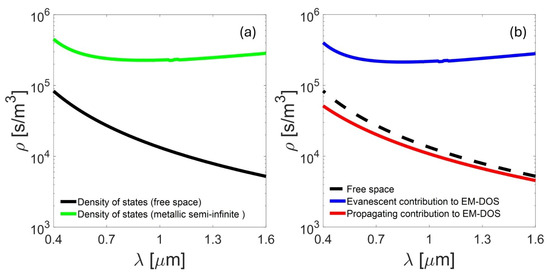
Figure 2.
EM-DOS spectra ranging from 400 nm to 1600 nm. (a) Comparison of EM-DOS between free space (reference) and a metallic (Au) semi-infinite surface at nm. (b) Contributions of propagating and evanescent components to the total EM-DOS relative to free space.
Figure 2a shows that EM-DOS measures the number of electromagnetic modes available for light–matter interactions at a given wavelength. The black curve follows an equation of the form . This behavior across spectral regions shows that the EM-DOS increases sharply as the wavelength decreases in the VIS region, indicating a higher density of states available for interaction in shorter wavelengths than in the IR region, where the density of states starts to decrease with increasing wavelength. This result shows that in free space, no physical boundaries or materials can confine or scatter the electromagnetic waves, as expected, so they can propagate freely in all directions, and due to the absence of material interfaces, the contribution of evanescent modes to the DOS is minimal or zero. Since free space lacks such interfaces, these modes are absent, and the propagating modes primarily determine the DOS. As a result, the propagating modes of EM-DOS define the dominant behavior of electromagnetic waves by increasing the availability of propagating modes. The use of free-space EM-DOS as a reference or baseline permits the study of the effects of different materials or structures on the behavior of the electromagnetic field. It represents the maximum possible propagative component to confine or scatter the field and is essential to understanding light–matter interactions across different parts of the spectrum. Free space, or vacuum, can be considered a dielectric material with some specific characteristics. In electromagnetics, free space is often treated as a dielectric with a dielectric constant equal to 1 and a relative permeability of 1. Introducing materials or structures interacting with electromagnetic fields can modify the value of the free-space EM-DOS. The simplest plasmonic structure is the metal–dielectric interface (Figure 2a). A metal–dielectric interface is the boundary between a metallic material (such as gold, silver, or aluminum) and a dielectric material such as free space, air, glass, or polymer. As shown in Figure 2a (green curve), a metal–dielectric interface significantly influences the EM-DOS. The excitation of SPPs near the metal–dielectric interface is directly related to the evanescent component of the EM-DOS at nm from the interface, as illustrated in Figure 2b (blue curve), having significant implications in nanophotonics and surface optics. At the interface, the presence of SPPs results in an increased field intensity near the surface due to the strong coupling between electromagnetic waves and the collective oscillations of free electrons in the metal, which leads to an increase in the density of states. Part of the EM-DOS (evanescent component, blue line) extends into the dielectric material resulting in the excitation of SPPs. This configuration enables the excitation of SPPs, manifesting when incident electromagnetic wave frequency aligns with the resonant frequency of the metallic structure governed by the SPP dispersion relationship, leading to significant electromagnetic field enhancements. This simple configuration allows researchers to manipulate and control light at the nanoscale. When light (photons) interacts with the metal surface, it can excite collective oscillations of free electrons in the metal. These oscillations are known as surface plasmons. Furthermore, the propagating component (red line) of EM-DOS remains unchanged, and its value is comparable to the total EM-DOS in a free space since the EM-DOS only consists of the propagating component. In the Introduction, we referred to the EM-DOS as a function of the distance (z) from the interface. In this context, the EM-DOS exhibits interesting behavior at different distances from a metal–dielectric interface, as illustrated in Figure 3.
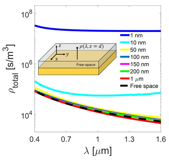
Figure 3.
EM-DOS spectra from 400 nm to 1600 nm for a punctual source positioned at varying distances from the Au surface. Notably, evanescent contributions to the EM-DOS are almost suppressed beyond 100 nm.
In Figure 3, we observe that EM-DOS varies significantly with the distance from the interface. EM-DOS decreases exponentially with the distance following the form expression. Near the interface, the electromagnetic fields linked to SPPs decrease exponentially as the distance from the surface increases. In this case, the penetration depth permits the quantification of this exponential decay of surface plasmon near the metallic–dielectric interface. At a metal–dielectric interface, the SPP penetration depth is measured for the distance over which the field amplitude decreases to of its value at the interface. It characterizes how deeply the electromagnetic field penetrates each material. The penetration depth affects the localization of the plasmonic field and determines how sensitive the SPPs are to changes in the surrounding environment, particularly in the free space or dielectric. In applications like sensing, penetration depth helps define the range over which surface plasmons can interact with molecules or particles near the interface, influencing sensitivity and specificity.
This concept is fundamental in plasmonic sensors and photonics applications since it affects how strongly the plasmonic field couples with external stimuli, like refractive index changes or fluorescent molecules. The relationship between penetration depth and EM-DOS is significant, especially in SPPs at a metal–dielectric interface. As we move far away from the interface, the strength of the electromagnetic fields decreases, leading to a reduction in the EM-DOS ( nm), and consequently, the evanescent component of EM-DOS decreases considerably. However, as we move to the interface, the contribution of these modes increases, leading to an increase in EM-DOS. In terms of the behavior of EM-DOS in the near field, it shows high sensitivity, with the distance to the interface being the evanescent component dominating the total EM-DOS. Several intrinsic factors influence the decrease in EM-DOS with distance from the interface. The confinement of SPPs to the interface results in a rapid electromagnetic field decay into both the metal and the dielectric, influencing the EM-DOS. Furthermore, metals with higher conductivity will have shorter penetration depths, leading to a faster decrease in EM-DOS. Quantum mechanical effects such as tunneling can affect the EM-DOS at very short distances. Finally, the geometry of the interface, such as roughness or nanostructuring, can also impact the EM-DOS, i.e., nanostructures can enhance local fields but typically only within a short range from the interface. The choice of metal is not just a decision but a fundamental one that directly influences the EM-DOS and, consequently, the plasmonic performance. This makes it a critical element in the design of efficient devices.
Figure 4a illustrates the EM-DOS at the metal–free-space interface for different metals at nm from the interface. We observe that copper responds better to EM-DOS in the VIS and NIR regions than silver, gold, and aluminum. Copper’s dielectric function has a higher resonance in these regions than gold, aluminum, and silver. Gold and silver are noble metals with strong surface plasmon resonances in the VIS region and favorable light–matter interaction regions, significantly impacting various applications. While metals like aluminum and copper are also utilized, their plasmonic responses are generally different and less optimal than noble metals [42]. Therefore, gold and silver are predominantly used in plasmonic devices and nanostructures in the visible (VIS) and infrared (IR) regions due to having a strongly localized surface plasmon resonance in the VIS and NIR regions [43] because they can efficiently confine and enhance electromagnetic fields at these wavelengths, which is crucial for applications like sensing.
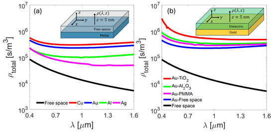
Figure 4.
Influence of material variations on EM-DOS spectra. (a) Comparison of free-space superstrate with various metallic substrates. (b) Comparison of a Au substrate with different superstrate dielectric media. All structures were illuminated with a punctual source placed at nm from the substrate surface.
The wavelength at which SPPs are excited varies among these metals. Metals exhibit different levels of damping losses, which influence the quality of the plasmonic resonance. The physical surface characteristics, such as surface roughness and morphology, can lead to differences in how the EM-DOS is enhanced or suppressed. The interaction of these metals with their surrounding environment (e.g., the dielectric medium) can further modify their plasmonic properties. These factors collectively explain how gold, silver, aluminum, and copper respond to the EM-DOS at the same distance from an interface, leading to their distinct plasmonic behaviors. However, the choice depends on specific requirements, cost considerations, and stability needs [44]. Plasmonic coupling occurs in different assemblies, such as gold nanorods, where the distance between them, orientation, and environment influence the EM-DOS, affecting the coupling between the plasmonic modes of nearby nanostructures. This understanding is crucial for designing and optimizing plasmonic devices with real-world applications. Researchers typically study the plasmonic properties of gold nanostructures across a broad range of wavelengths, primarily from the visible (VIS) to near-infrared (NIR) regions [45]. We previously studied how metals affect the EM-DOS at the metal–vacuum interface. Gold is ideal for various applications, such as sensors, imaging, and medical therapies, due to its high-efficiency excitation for surface plasmon resonance. Furthermore, its chemical stability and biocompatibility are appealing in scientific research and technological advancements. We will explore how dielectrics impact EM-DOS when we replace the free space with a dielectric material [46]. In general, dielectric materials have a refractive index greater than free space. For this purpose, we investigate the metallic (Au) semi-infinite surface for different dielectric materials: PMMA (polymethyl methacrylate), (aluminum oxide), and Ti (titanium dioxide). PMMA is a transparent polymer that does not affect plasmonic properties, boosts plasmonic coupling and protects metals, and Ti enhances light absorption and charge separation, making it useful for reduction and solar energy conversion.
Figure 4b shows the EM-DOS spectra for a metal–dielectric interface configuration at nm. Replacing free space with a dielectric material in a metallic plane configuration (blue) increases the EM-DOS. Ti has slightly higher EM-DOS than and PMMA due to Ti having a higher refractive index than and PMMA, leading to stronger electromagnetic field confinement near the interface that is more effective than free space. This confinement leads to a higher density of electromagnetic modes near the dielectric material. As a result, enhancing the EM-DOS can improve the spontaneous emission rates of QEs placed near the dielectric. The surrounding dielectric environment can influence the EM-DOS. The use of dielectric materials modifies the plasmonic response. For instance, different dielectric coatings or substrates can shift the resonance frequencies. Under certain conditions, some dielectric materials can create photonic bandgaps, which are frequency ranges where electromagnetic waves cannot propagate through the material [46]. At the edges of these bandgaps, the EM-DOS significantly enhances the presence of localized modes. We can exploit this effect to control the emission properties of QEs.
The metallic semi-infinite medium can be modified to tune the EM-DOS to desired frequencies by replacing the metallic plane with an array of nanoholes or nanopillars (Figure 1c,d) [47]. Generically speaking, an array of nanoholes or nanopillars refers to a structured arrangement of tiny holes or pillars on a surface, typically at the nanoscale (less than 100 nanometers). We calculate EM-DOS using the effective bulk permittivity concept. Nanostructures are modeled as homogeneous materials. This approach simplifies the complex interactions by averaging the properties of the nanostructures and the surrounding medium. The effective refractive index considers the overall response of the structure to electromagnetic fields without considering scattering effects. This effective permittivity depends on factors like the filling fraction, shape, and arrangement of the nanostructures, as well as the dielectric properties of the materials involved. This way of modeling is handy for designing and optimizing plasmonic devices. However, the analysis is limited to measurements far from the interface where local effects in the near field can be negligible. Light interacting with nanohole and nanopillar arrays generates localized surface plasmons, significantly influencing the EM-DOS [48,49]. The effective medium theory does not consider specific effects, such as scattering, resulting from interactions between individual nanostructures and imperfections within the array. We describe these nanostructures as composite materials made of different substances with distinct permittivities, and , particularly in their interaction with light. Typically, they consist of an ordered array of sub-wavelength-sized holes or pillars embedded in a thin film or substrate, usually on the nanometer scale. Our analysis uses the Maxwell Garnett method [50], which models the array as an effective medium with a permittivity determined by its geometry, material properties, surrounding medium, and periodicity. We express the effective permittivities for p- and s-polarized electromagnetic waves as follows [51]:
where f denotes the filling fraction, defined as the ratio of the volume (or area, in the 2D case) occupied by the inclusions (holes or pillars) to the total volume (or unit-cell area) of the array. Additionally, and represent the permittivity of the host and filling material, respectively.
Figure 5 illustrates the effective permittivity as a function of the filling fraction for metallic nanohole and nanopillar arrays under p-polarized light. The filling fraction denotes the proportion of the total area occupied by a nanohole or nanopillar within the array characterized by the unit cell. In Figure 5a, we observe that the nanohole array shows zero permittivity at a filling fraction of 85% because the high density of nanoholes disrupts the continuity of the metal. This phenomenon is linked to the Extraordinary Optical Transmission effect, where the nanoholes allow enhanced transmission of light through the metal film. A nanopillar array, in turn, exhibits a pole in permittivity at a similar filling fraction, around 85%, for p polarization. This is due to the resonant modes supported by the nanopillars. At this filling fraction, the interaction between the electromagnetic field and the nanopillars is maximized, leading to a resonance condition where the permittivity diverges (poles). Shape, size, and arrangement of the nanopillars create localized surface plasmon resonances. Although the model predicts a singularity of the effective permittivity, real experiments show a smoothed resonance. This is mainly due to scattering and nonlocal effects from nanostructures, which increase the damping and broaden the imaginary part around the resonance.
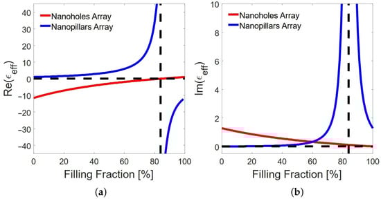
Figure 5.
(a) Real and (b) imaginary parts of the effective dielectric permittivity as a function of the filling fraction for metallic nanohole and nanopillar arrays, under p-polarized light. The nanohole array exhibits zero permittivity at a filling fraction of 85%. Also, the nanopillar array shows a pole at a filling fraction of around 85%. The horizontal dashed black lines signal zero of the real and imaginary parts of the effective dielectric permittivity. The vertical dashed black lines signal the filling value where the real part of the effective dielectric permitivity of the nanohole array crosses zero, around 85%.
Similarly, Figure 6 shows the effective dielectric permittivity as a function of the filling fraction for metallic nanohole and nanopillar arrays under s-polarized light. We observe in Figure 6a that the effective dielectric permittivity of an array of nanoholes is equal to that of an array of nanopillars, except that this effective dielectric permittivity is reflected around the central value of the filling fraction variable of 50%, or . An array of nanoholes with a filling fraction f contains the same ratios of metal and dielectric as an array of nanopillars with filling fraction , which is the transformation that leads to this reflection. This match suggests that the geometric arrangement of the nanostructures does not significantly alter the effective permittivity in this polarization state; the crucial variable is the ratio of metal to dielectric in the arrays. This can be attributed to s-polarized light interacting similarly with both structures, leading to comparable effective medium responses. For both nanostructures, the disruption in the continuity of the metallic plane leads to a situation where the effective medium behaves as if it has zero permittivity. Similarly, both nanostructures are also reflected around in the complex part of the effective dielectric remittance. This is very interesting because nanohole and nanopillar arrays exhibit similar behavior for the complex part of the effective dielectric permittivity under s-polarized light, suggesting that their loss mechanisms and interaction with the electromagnetic field are comparable. Hence, it accounts for absorption and scattering losses and is influenced more by the material properties and less by the specific geometry of the nanostructures in this polarization state.
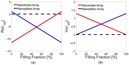
Figure 6.
(a) Real and (b) imaginary parts of the effective dielectric permittivity as a function of the filling fraction for metallic nanohole and nanopillar arrays, under s-polarized light. Nanohole arrays exhibit zero permittivity at a filling fraction of 95% whereas nanopillar arrays achieve this at a filling fraction of 5%. The horizontal dashed black lines signal zero of the real and imaginary parts of the effective dielectric permittivity.
The difference in permittivity between nanohole and nanopillar arrays under p and s polarization is due to their unique interactions with electromagnetic waves. In nanohole arrays, p polarization (parallel to the plane of incidence) strongly couples with surface plasmon polaritons (SPPs) at the metal–dielectric interface, while s polarization (perpendicular) interacts less with SPPs, leading to different permittivity values. Permittivity changes in nanopillar arrays under p and s polarization can be explained by resonance behavior as a consequence of the pillars’ shapes and orientations, which are the unique geometries of each nanostructure that shape its response to different polarizations, influencing permittivity. The real and imaginary components of permittivity influence the electromagnetic density of states (EM-DOS). In contrast, the real component shapes the propagation characteristics and available modes, and the imaginary component governs the absorption and loss, which are crucial for determining the EM-DOS. Our discussion about the EM-DOS of periodic nanohole and nanopillar array structure with Equations (11) and (12) is for .
In both cases, the filling fraction, f, depends on the radius r of the nanohole or nanopillar and the period P of the array, . Calculating EM-DOS by placing a QE, such as a dipole source at a distance z from the surface, is a powerful method for evaluating nanostructures. The distance z can be varied to study its effect on the EM-DOS.
Figure 7 shows the EM-DOS for a punctual source at different distances above the surface for different plasmonic structures at different distances. The filling fraction was set to 30% for nanohole and nanopillar arrays. The EM-DOS spectrum for a QE placed 1 nm from different gold nanostructures (flat semi-infinite medium, nanohole array, and nanopillar array) in the range from 400 nm to 1600 nm exhibit distinct behaviors due to the unique interactions with each structure. EM-DOS at 1 nm from the interface is more significant than nanopillar arrays at shorter wavelengths compared to a semi-infinite metallic plane and nanohole arrays. These structures support various resonant modes, including Mie and guided mode resonances. These resonances can significantly enhance the local electromagnetic fields, leading to a higher EM-DOS. The shape and size of the nanopillars can be optimized to resonate at specific wavelengths within the visible spectrum. When the periodicity of a nanostructure matches the wavelength of the incident light, surface lattice resonance modes emerge, leading to a significant enhancement of EM-DOS [52].
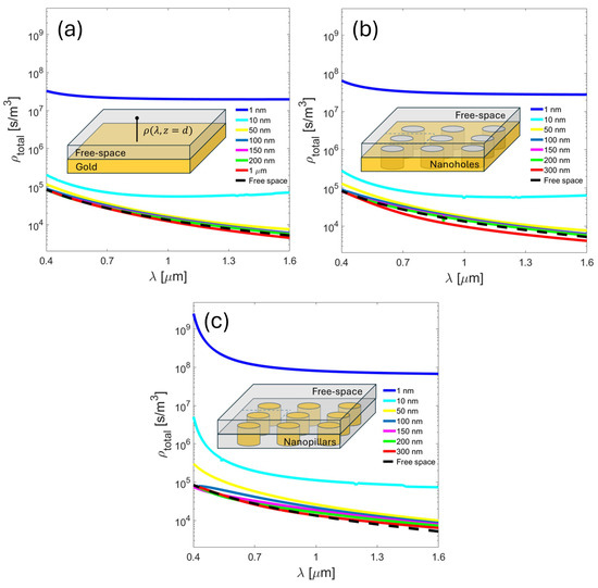
Figure 7.
EM-DOS for a punctual source at different distances above the surface for different plasmonic structures at different distances. The gold-dielectric flat interface is displayed in panel (a), the nanohole array is displayed in panel (b) and the nanopillar array is displayed in panel (c). The filling fraction was set to 30% for nanohole and nanopillar arrays.
Unlike flat surfaces that can support SPPs, the enhancement is generally less pronounced compared to the localized resonances in nanopillars. Furthermore, the nanohole array can support localized surface plasmon resonances and diffractive coupling of SPPs, but the enhancement is typically more distributed and less intense than the localized resonances in nanopillars. The geometry of nanopillars allows for strong confinement of electromagnetic fields at their surfaces, leading to higher local field intensities and, thus, a greater EM-DOS. In the case of a flat semi-infinite metallic medium, the field confinement is less effective than nanopillars, resulting in a lower EM-DOS. However, although nanoholes can confine fields, the confinement is generally less effective than in nanopillars due to the different geometrical constraints. However, although nanoholes can confine fields, the confinement is generally less effective than in nanopillars due to the different geometrical constraints. The interaction of light with the nanopillars can lead to enhanced EM-DOS for specific polarizations and incident angles. Due to anisotropy, this type of nanostructure can be exploited to achieve higher EM-DOS in the visible region. In the flat semi-infinite, the interaction is more uniform and less dependent on specific geometrical features, resulting in a lower overall enhancement. The nanohole array’s periodicity can lead to complex interactions, but the overall enhancement is typically less than that of nanopillars. Beyond 150 nm, EM-DOS spectra are mainly affected by propagative modes, with no contribution from evanescent components in all plasmonic structures.
The concept of effective permittivity for nanostructured media such as a nanohole or nanopillar array applies only at distances with negligible near-field effects. We calculate the decay constant from EM-DOS measured at various distances, z, from the interface to the source. Plotting the decay curve, we identify the distance where the decay curve matches that in free space. This provides us with a straightforward way to determine the effective distance for applying the permittivity of a nanostructured medium, ensuring accurate modeling and analysis.
Figure 8 illustrates the use of the method to find the distance where the decay curve matches that in free space for semi-infinite metallic medium, nanohole, and nanopillar arrays at a wavelength of 630 nm. For this analysis, we assume that near-field scattering effects close to the surface are negligible, meaning that the nanostructure is treated as a bulk material with an effective permittivity given by Equations (11) and (12). Figure 8a shows how the decay curve of a source to a gold semi-infinite surface depends significantly on the distance to the interface. The source is in the near-field region at very short distances (1 to 10 nm). In this region, the surface plasmons strongly influence the electromagnetic field. This leads to a significant enhancement of EM-DOS, resulting in a higher decay rate for the source. As the distance increases (10 to 100 nm), the influence of the near-field effects diminishes. Therefore, the decay rate decreases as the source moves away from the intense field enhancement region. However, the source can still interact with the evanescent fields, which can moderately enhance the decay rate compared to free space. In the far field, at more considerable distances (100 nm away), the source is in the far-field region. Here, the influence of the nanostructured material on the EM-DOS is minimal, and the decay rate approaches that of the source in free space. The decay curve flattens out, indicating that the emitter’s spontaneous emission rate is no longer significantly affected by the presence of the nanostructures. This information is crucial for designing plasmonic devices and optimizing their performance for sensing, imaging, and quantum technology applications. Figure 8b illustrates a comparison of decay rates for gold semi-infinite medium (red), nanohole (blue), and nanopillar (green) arrays with the source located 300 nm above the surface for a wavelength of 630 nm. At this distance, the near-field effects due to the evanescent component no longer contribute to EM-DOS.
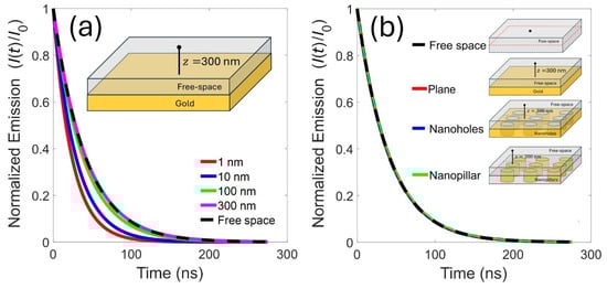
Figure 8.
(a) Normalized emission as a function of time with the source placed at different distances from the surface for a a semi-infinite metallic medium. (b) Comparison of normalized emissions for semi-infinite metallic medium (red), nanohole (blue), and nanopillar (green) arrays with the source located 300 nm above the surface for a wavelength of 630 nm. These normalized emissions are obtained from a mono-exponential decay, , and the corresponding decay rates, which are obtained from Equation (10).
4. Conclusions
In summary, EM-DOS is a physical quantity fundamental in applications like sensors and quantum technologies. It is dependent on the distance to the interface. It is a tool that can be used where precise control over these interactions can lead to significant performance improvements. EM-DOS at metal–dielectric interfaces is crucial for optimizing light–matter interactions. Two basic nanostructures, nanoholes and nanopillar arrays, were analyzed using the EM-DOS and the concept of effective permittivity. These structures can enhance localized resonances by tuning the EM-DOS to specific frequencies, with nanopillars often providing stronger localized resonances than nanoholes. This makes them highly effective in various plasmonic applications. The effective permittivity approach is a valuable tool for simplifying the modeling of these complex structures, allowing for more straightforward analysis and design. We extend the application of the definition of EM-DOS to determine the distance at which nanostructures behave like bulk materials. We use the decay curve method to optimize the device design and performance, ensuring that the nanostructures are utilized to their full potential, which manifests the evanescent nature of the modes excited on the metal surface, providing an insight into how quickly the energy of these modes diminishes with distance from the interface, which is crucial for sensing, imaging, and nanophotonics applications.
Author Contributions
Conceptualization, R.C.-M.; methodology and validation, R.C.-M. and R.T.-L.; investigation, R.C.-M. and R.T.-L.; writing, R.C.-M., R.T.-L., C.E.G.-O., B.R.J.-Á. and G.A.G.-M.; visualization, R.C.-M., R.T.-L., and B.R.J.-Á.; project administration, R.C.-M. and G.A.G.-M.; funding acquisition, R.C.-M. All authors have read and agreed to the published version of the manuscript.
Funding
This research was partially funded by CONAHCYT (Basic Scientific Research Grant A1-S-13587).
Institutional Review Board Statement
Not applicable.
Informed Consent Statement
Not applicable.
Data Availability Statement
The data presented in this study are available upon request to the corresponding author.
Conflicts of Interest
The authors declare no conflicts of interest.
Abbreviations
The following abbreviations are used in this manuscript:
| DOS | Density of States |
| EM-DOS | Electromagnetic Density of States |
| NV | Nitrogen Vacancy |
| PMMA | Poly(Methyl Methacrylate) |
| QE | Quantum Emitter |
| SPP | Surface Plasmon Polariton |
| SPR | Surface Plasmon Resonance |
References
- Wen, B.Y.; Wang, J.Y.; Shen, T.L.; Zhu, Z.W.; Guan, P.C.; Lin, J.S.; Peng, W.; Cai, W.W.; Jin, H.; Xu, Q.C.; et al. Manipulating the light-matter interactions in plasmonic nanocavities at 1 nm spatial resolution. Light. Sci. Appl. 2022, 11, 235. [Google Scholar] [CrossRef]
- Zundel, L.; Gieri, P.; Sanders, S.; Manjavacas, A. Comparative Analysis of the Near- and Far-Field Optical Response of Thin Plasmonic Nanostructures. Adv. Opt. Mater. 2022, 10, 2102550. [Google Scholar] [CrossRef]
- Shahbazyan, T.V. Local Density of States for Nanoplasmonics. Phys. Rev. Lett. 2016, 117, 207401. [Google Scholar] [CrossRef]
- Messina, R.; Hugonin, J.P.; Greffet, J.J.; Marquier, F.m.c.; De Wilde, Y.; Belarouci, A.; Frechette, L.; Cordier, Y.; Ben-Abdallah, P. Tuning the electromagnetic local density of states in graphene-covered systems via strong coupling with graphene plasmons. Phys. Rev. B 2013, 87, 085421. [Google Scholar] [CrossRef]
- Vaskin, A.; Kolkowski, R.; Koenderink, A.F.; Staude, I. Light-emitting metasurfaces. Nanophotonics 2019, 8, 1151–1198. [Google Scholar] [CrossRef]
- Chao, P.; Defo, R.K.; Molesky, S.; Rodriguez, A. Maximum electromagnetic local density of states via material structuring. Nanophotonics 2023, 12, 549–557. [Google Scholar] [CrossRef]
- Nefedov, I.S.; Viitanen, A.J.; Tretyakov, S.A. Propagating and evanescent modes in two-dimensional wire media. Phys. Rev. E 2005, 71, 046612. [Google Scholar] [CrossRef]
- Huang, L.; Chen, X.; Mühlenbernd, H.; Zhang, H.; Chen, S.; Bai, B.; Tan, Q.; Jin, G.; Cheah, K.W.; Qiu, C.W.; et al. Three-dimensional optical holography using a plasmonic metasurface. Nat. Commun. 2013, 4, 2808. [Google Scholar] [CrossRef]
- Lucchesi, C.; Vaillon, R.; Chapuis, P.O. Radiative heat transfer at the nanoscale: Experimental trends and challenges. Nanoscale Horiz. 2021, 6, 201–208. [Google Scholar] [CrossRef] [PubMed]
- Babicheva, V.E. Optical Processes behind Plasmonic Applications. Nanomaterials 2023, 13, 1270. [Google Scholar] [CrossRef]
- Wei, Q.; Bi, D.; Qi, X.; Ren, M.; Wu, F. Angle-independent topological interface states in one-dimensional photonic crystal heterostructures containing hyperbolic metamaterials. Opt. Lett. 2025, 50, 451. [Google Scholar] [CrossRef]
- Lequeux, M.; Mele, D.; Venugopalan, P.; Gillibert, R.; Boujday, S.; Knoll, W.; Dostalek, J.; Lamy de la Chapelle, M. Plasmonic Properties of Gold Nanostructures on Gold Film. Plasmonics 2020, 15, 1653–1660. [Google Scholar] [CrossRef]
- Singh, G.P.; Sardana, N. Smartphone-based Surface Plasmon Resonance Sensors: A Review. Plasmonics 2022, 17, 1869–1888. [Google Scholar] [CrossRef]
- Yang, S.; Zhou, R.L.; Huang, Y.J. Surface plasmon resonance and field confinement in graphene nanoribbons in a nanocavity. Front. Phys. 2021, 16, 43504. [Google Scholar] [CrossRef]
- Garcia-Vidal, F.J.; Fernández-Domínguez, A.I.; Martin-Moreno, L.; Zhang, H.C.; Tang, W.; Peng, R.; Cui, T.J. Spoof surface plasmon photonics. Rev. Mod. Phys. 2022, 94, 025004. [Google Scholar] [CrossRef]
- Qian, Z.; Shan, L.; Zhang, X.; Liu, Q.; Ma, Y.; Gong, Q.; Gu, Y. Spontaneous emission in micro- or nanophotonic structures. PhotoniX 2021, 2, 21. [Google Scholar] [CrossRef]
- Diguna, L.J.; Tjahjana, L.; Darma, Y.; Zeng, S.; Wang, H.; Birowosuto, M.D. Light–Matter Interaction of Single Quantum Emitters with Dielectric Nanostructures. Photonics 2018, 5, 14. [Google Scholar] [CrossRef]
- Ciracì, C.; Jurga, R.; Khalid, M.; Sala, F.D. Plasmonic quantum effects on single-emitter strong coupling. Nanophotonics 2019, 8, 1821–1833. [Google Scholar] [CrossRef]
- Lee, Y.M.; Kim, S.E.; Park, J.E. Strong coupling in plasmonic metal nanoparticles. Nano Converg. 2023, 10, 34. [Google Scholar] [CrossRef] [PubMed]
- Liu, J.; Chen, G.; Li, L.; Liu, R.; Li, W.; Liu, G.; Wu, F.; Chen, Y. Radiative coupling of two quantum emitters in arbitrary metallic nanostructures. Sci. Rep. 2022, 12, 6901. [Google Scholar] [CrossRef]
- González-Tudela, A.; Huidobro, P.A.; Martín-Moreno, L.; Tejedor, C.; García-Vidal, F.J. Reversible dynamics of single quantum emitters near metal-dielectric interfaces. Phys. Rev. B 2014, 89, 041402. [Google Scholar] [CrossRef]
- Ge, D.; Marguet, S.; Issa, A.; Jradi, S.; Nguyen, T.H.; Nahra, M.; Béal, J.; Deturche, R.; Chen, H.; Blaize, S.; et al. Hybrid plasmonic nano-emitters with controlled single quantum emitter positioning on the local excitation field. Nat. Commun. 2020, 11, 3414. [Google Scholar] [CrossRef]
- Acosta, V.; Hemmer, P. Nitrogen-vacancy centers: Physics and applications. MRS Bull. 2013, 38, 127–130. [Google Scholar] [CrossRef]
- Riedel, D.; Söllner, I.; Shields, B.J.; Starosielec, S.; Appel, P.; Neu, E.; Maletinsky, P.; Warburton, R.J. Deterministic Enhancement of Coherent Photon Generation from a Nitrogen-Vacancy Center in Ultrapure Diamond. Phys. Rev. X 2017, 7, 031040. [Google Scholar] [CrossRef]
- Westmoreland, D.E.; McClelland, K.P.; Perez, K.A.; Schwabacher, J.C.; Zhang, Z.; Weiss, E.A. Properties of quantum dots coupled to plasmons and optical cavities. J. Chem. Phys. 2019, 151, 210901. [Google Scholar] [CrossRef]
- Bitton, O.; Gupta, S.N.; Haran, G. Quantum dot plasmonics: From weak to strong coupling. Nanophotonics 2019, 8, 559–575. [Google Scholar] [CrossRef]
- Hertzog, M.; Wang, M.; Mony, J.; Börjesson, K. Strong light–matter interactions: A new direction within chemistry. Chem. Soc. Rev. 2019, 48, 937–961. [Google Scholar] [CrossRef]
- Singh, S.; Singh, P.K.; Umar, A.; Lohia, P.; Albargi, H.; Castañeda, L.; Dwivedi, D.K. 2D Nanomaterial-Based Surface Plasmon Resonance Sensors for Biosensing Applications. Micromachines 2020, 11, 779. [Google Scholar] [CrossRef]
- Wong, C.L.; Olivo, M. Surface Plasmon Resonance Imaging Sensors: A Review. Plasmonics 2014, 9, 809–824. [Google Scholar] [CrossRef]
- Arakawa, Y.; Holmes, M.J. Progress in quantum-dot single photon sources for quantum information technologies: A broad spectrum overview. Appl. Phys. Rev. 2020, 7, 021309. [Google Scholar] [CrossRef]
- Lepeshov, S.; Gorodetsky, A.; Krasnok, A.; Rafailov, E.; Belov, P. Enhancement of terahertz photoconductive antenna operation by optical nanoantennas. Laser Photonics Rev. 2017, 11, 1600199. [Google Scholar] [CrossRef]
- Li, X.; Mengu, D.; Yardimci, N.T.; Turan, D.; Charkhesht, A.; Ozcan, A.; Jarrahi, M. Plasmonic photoconductive terahertz focal-plane array with pixel super-resolution. Nat. Photonics 2024, 18, 139. [Google Scholar] [CrossRef]
- Yardimci, N.T.; Yang, S.H.; Berry, C.W.; Jarrahi, M. High-Power Terahertz Generation Using Large-Area Plasmonic Photoconductive Emitters. IEEE Trans. Terahertz Sci. Technol. 2015, 5, 223. [Google Scholar] [CrossRef]
- Zhou, T.; Wang, T.B.; Liao, Q.H.; Liu, J.T.; Yu, T.B.; Liu, N.H. Electromagnetic local density of states in graphene-covered porous silicon carbide. Phys. Lett. A 2017, 381, 1976–1980. [Google Scholar] [CrossRef]
- Joulain, K.; Carminati, R.; Mulet, J.P.; Greffet, J.J. Definition and measurement of the local density of electromagnetic states close to an interface. Phys. Rev. B 2003, 68, 245405. [Google Scholar] [CrossRef]
- Ida, N. Reflection and Transmission of Plane Waves. In Engineering Electromagnetics; Springer International Publishing: Cham, Switzerland, 2021; pp. 651–707. [Google Scholar] [CrossRef]
- Savi, P.; Bertoldo, S.; Milani, A. Determining real permittivity from Fresnel coefficients in GNSS-R. Prog. Electromagn. Res. M 2019, 79, 159–166. [Google Scholar] [CrossRef]
- Li, Y. Plasmonic Optics: Theory and Applications; SPIE Press: Bellingham, WA USA, 2017. [Google Scholar] [CrossRef]
- Novotny, L.; Hecht, B. Optical interactions. In Principles of Nano-Optics; Cambridge University Press: Cambridge, UK, 2012; pp. 224–281. [Google Scholar]
- Henkel, C.; Pötting, S.; Wilkens, M. Loss and heating of particles in small and noisy traps. Appl. Phys. B 1999, 69, 379–387. [Google Scholar] [CrossRef]
- Ferrier, L.; Bouteyre, P.; Pick, A.; Cueff, S.; Dang, N.H.M.; Diederichs, C.; Belarouci, A.; Benyattou, T.; Zhao, J.X.; Su, R.; et al. Unveiling the Enhancement of Spontaneous Emission at Exceptional Points. Phys. Rev. Lett. 2022, 129, 083602. [Google Scholar] [CrossRef] [PubMed]
- Oliveira, L.C.; Herbster, A.; da Silva Moreira, C.; Neff, F.H.; Lima, A.M.N. Surface Plasmon Resonance Sensing Characteristics of Thin Aluminum Films in Aqueous Solution. IEEE Sens. J. 2017, 17, 6258–6267. [Google Scholar] [CrossRef]
- Aftab, M.; Mansha, M.S.; Iqbal, T.; Farooq, M. Surface Plasmon Excitation: Theory, Configurations, and Applications. Plasmonics 2024, 19, 1701–1719. [Google Scholar] [CrossRef]
- Pandey, S.; Singh, S.; Lohia, P.; Yadav, R.K.; Dwivedi, D. Comparative study of Au, Al, and Ag metal based SPR sensor using nickel and antimonene to enhance the sensitivity in visible range. Res. Sq. 2022. [Google Scholar] [CrossRef]
- Ghosh, P.K.; Debu, D.T.; French, D.A.; Herzog, J.B. Calculated thickness dependent plasmonic properties of gold nanobars in the visible to near-infrared light regime. PLoS ONE 2017, 12, e0177463. [Google Scholar] [CrossRef]
- Hasan, S.B.; Mosk, A.P.; Vos, W.L.; Lagendijk, A. Finite-size Scaling of the Density of States in Photonic Band Gap Crystals. Phys. Rev. Lett. 2018, 120, 237402. [Google Scholar] [CrossRef]
- Patti, T.L.; Wild, D.S.; Shahmoon, E.; Lukin, M.D.; Yelin, S.F. Controlling Interactions between Quantum Emitters Using Atom Arrays. Phys. Rev. Lett. 2021, 126, 223602. [Google Scholar] [CrossRef] [PubMed]
- Vu Thi, D.; Ohno, T.; Yamamoto, N.; Sannomiya, T. Field localization of hexagonal and short-range ordered plasmonic nanoholes investigated by cathodoluminescence. J. Chem. Phys. 2020, 152, 074707. [Google Scholar] [CrossRef]
- Peng, X.; Poelker, M.; Stutzman, M.; Tang, B.; Zhang, S.; Zou, J. Mie-type GaAs nanopillar array resonators for negative electron affinity photocathodes. Opt. Express 2020, 28, 860–874. [Google Scholar] [CrossRef] [PubMed]
- Markel, V.A. Introduction to the Maxwell Garnett approximation: Tutorial. J. Opt. Soc. Am. A 2016, 33, 1244–1256. [Google Scholar] [CrossRef] [PubMed]
- Sareni, B.; Krähenbühl, L.; Beroual, A.; Brosseau, C. Effective dielectric constant of periodic composite materials. J. Appl. Phys. 1996, 80, 1688–1696. [Google Scholar] [CrossRef]
- Sanders, S.; Dowran, M.; Jain, U.; Lu, T.M.; Marino, A.M.; Manjavacas, A. Lattice Resonances of Nanohole Arrays for Quantum Enhanced Sensing. Phys. Rev. Appl. 2022, 17, 014035. [Google Scholar] [CrossRef]


Disclaimer/Publisher’s Note: The statements, opinions and data contained in all publications are solely those of the individual author(s) and contributor(s) and not of MDPI and/or the editor(s). MDPI and/or the editor(s) disclaim responsibility for any injury to people or property resulting from any ideas, methods, instructions or products referred to in the content. |
© 2025 by the authors. Licensee MDPI, Basel, Switzerland. This article is an open access article distributed under the terms and conditions of the Creative Commons Attribution (CC BY) license (https://creativecommons.org/licenses/by/4.0/).